EP1170819A2 - Dualmode Bandpassfilter - Google Patents
Dualmode Bandpassfilter Download PDFInfo
- Publication number
- EP1170819A2 EP1170819A2 EP01111072A EP01111072A EP1170819A2 EP 1170819 A2 EP1170819 A2 EP 1170819A2 EP 01111072 A EP01111072 A EP 01111072A EP 01111072 A EP01111072 A EP 01111072A EP 1170819 A2 EP1170819 A2 EP 1170819A2
- Authority
- EP
- European Patent Office
- Prior art keywords
- dielectric body
- band pass
- pass filter
- metal film
- dual mode
- Prior art date
- Legal status (The legal status is an assumption and is not a legal conclusion. Google has not performed a legal analysis and makes no representation as to the accuracy of the status listed.)
- Granted
Links
- 230000009977 dual effect Effects 0.000 title claims abstract description 84
- 239000002184 metal Substances 0.000 claims abstract description 92
- 229910052751 metal Inorganic materials 0.000 claims abstract description 92
- 230000008878 coupling Effects 0.000 claims abstract description 44
- 238000010168 coupling process Methods 0.000 claims abstract description 44
- 238000005859 coupling reaction Methods 0.000 claims abstract description 44
- QNRATNLHPGXHMA-XZHTYLCXSA-N (r)-(6-ethoxyquinolin-4-yl)-[(2s,4s,5r)-5-ethyl-1-azabicyclo[2.2.2]octan-2-yl]methanol;hydrochloride Chemical compound Cl.C([C@H]([C@H](C1)CC)C2)CN1[C@@H]2[C@H](O)C1=CC=NC2=CC=C(OCC)C=C21 QNRATNLHPGXHMA-XZHTYLCXSA-N 0.000 claims description 5
- 230000005684 electric field Effects 0.000 description 11
- 230000001902 propagating effect Effects 0.000 description 5
- 230000005540 biological transmission Effects 0.000 description 3
- 238000000034 method Methods 0.000 description 2
- 238000004891 communication Methods 0.000 description 1
- 239000002131 composite material Substances 0.000 description 1
- 239000003989 dielectric material Substances 0.000 description 1
- 238000009792 diffusion process Methods 0.000 description 1
- 238000009826 distribution Methods 0.000 description 1
- 230000005672 electromagnetic field Effects 0.000 description 1
- 230000000149 penetrating effect Effects 0.000 description 1
- 230000000007 visual effect Effects 0.000 description 1
Images





Classifications
-
- H—ELECTRICITY
- H01—ELECTRIC ELEMENTS
- H01P—WAVEGUIDES; RESONATORS, LINES, OR OTHER DEVICES OF THE WAVEGUIDE TYPE
- H01P7/00—Resonators of the waveguide type
- H01P7/08—Strip line resonators
-
- H—ELECTRICITY
- H01—ELECTRIC ELEMENTS
- H01P—WAVEGUIDES; RESONATORS, LINES, OR OTHER DEVICES OF THE WAVEGUIDE TYPE
- H01P1/00—Auxiliary devices
- H01P1/20—Frequency-selective devices, e.g. filters
- H01P1/201—Filters for transverse electromagnetic waves
- H01P1/203—Strip line filters
- H01P1/20327—Electromagnetic interstage coupling
- H01P1/20354—Non-comb or non-interdigital filters
- H01P1/20381—Special shape resonators
-
- H—ELECTRICITY
- H01—ELECTRIC ELEMENTS
- H01P—WAVEGUIDES; RESONATORS, LINES, OR OTHER DEVICES OF THE WAVEGUIDE TYPE
- H01P7/00—Resonators of the waveguide type
- H01P7/08—Strip line resonators
- H01P7/082—Microstripline resonators
-
- H—ELECTRICITY
- H01—ELECTRIC ELEMENTS
- H01P—WAVEGUIDES; RESONATORS, LINES, OR OTHER DEVICES OF THE WAVEGUIDE TYPE
- H01P7/00—Resonators of the waveguide type
- H01P7/08—Strip line resonators
- H01P7/084—Triplate line resonators
Definitions
- the present invention relates to dual mode band pass filters preferably used as, for example, band filters incorporated in communication apparatuses for high frequency bands ranging from a microwave band to a millimeter-wave band.
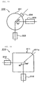
- Figs. 13 and 14 show schematic plan views for illustrating conventional dual mode band pass filters.
- a circular conductive film 201 is disposed on a dielectric body (not shown).
- the conductive film 201 is coupled to input/output coupling circuits 202 and 203 arranged to define an angle of 90 degrees.
- a top-end open stub 204 is arranged to form a central angle of 45 degrees with the position where the input/output coupling circuit 203 is arranged. With this arrangement, two resonance modes having different resonance frequencies are mutually coupled.
- the band pass filter 200 functions as a dual mode band pass filter.
- a square conductive film 211 is disposed on a dielectric body.
- the conductive film 211 is coupled to input/output coupling circuits 212 and 213 defining an angle of about 90 degrees. A corner defining an angle of about 135 degrees with the input/output coupling circuit 213 is cut away. By disposing a cut-away portion 211a, two resonance modes have different resonance frequencies. With this arrangement, since the two resonance modes are mutually coupled, the band pass filter 210 functions as a dual mode band pass filter.
- a ring-shaped conductive film is used in dual mode band pass filters (Japanese Unexamined Patent Application Publication No. 9-139612, Japanese Unexamined Patent Application Publication No. 9-162610, etc.).
- dual mode band pass filters Japanese Unexamined Patent Application Publication No. 9-139612, Japanese Unexamined Patent Application Publication No. 9-162610, etc.
- input/output coupling circuits are arranged at a central angle of 90 degrees, and a top-end open stub is disposed in a portion of the ring-shaped transmission line.
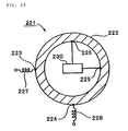
- a dual mode filter 221 includes a ring-shaped resonator defined by disposing a ring-shaped conductive film 222 on a dielectric body.
- each of the four terminals 223 to 226 is arranged to define an angle of 90 degrees with the ring-shaped conductive film 222.
- the two terminals 223 and 224 defining an angle of 90 degrees are coupled to input/output coupling circuits 227 and 228.
- the remaining two terminals 225 and 226 are connected to each other via a feedback circuit 230.
- the conductive film 201 has a circular shape.
- the conductive film 211 has a square shape.
- the shapes of the conductive films are restricted. As a result, there is little freedom of design.
- preferred embodiments of the present invention provide a dual mode band pass filter that achieves miniaturization, facilitates adjustments of the coupling strength, achieves a wider pass band and greatly improves the freedom of design.
- a dual mode band pass filter including a dielectric body having a first main surface and a second main surface, a metal film partially disposed on the first main surface or at a certain height position in the dielectric body, at least one ground electrode disposed on the second main surface or inside the dielectric body in such a manner that the metal film is opposed to the ground electrode via a portion of the dielectric body, and a pair of input/output coupling circuits coupled to different parts of the metal film.
- the two resonance modes are generated in a direction that is substantially parallel to a virtual line connecting the portions coupling the pair of input/output coupling circuits to the metal film and in a direction that is substantially to the virtual line.
- relative permittivities of the portions of the dielectric body in the region where the metal film is opposed to the ground electrode via the dielectric body are made different from the relative permittivity of the remaining portion.
- one of the two resonance modes is influenced by the dielectric-body portions having the different relative permittivities, and the resonance frequency of the influenced resonance mode thereby changes.
- the two resonance modes are mutually coupled. That is, since the portions of the dielectric body have different relative permittivities from that of the remaining portion, the band pass filter functions as a dual mode band pass filter.
- the portions of the dielectric body having the different relative permittivities may be cavities formed in the dielectric body.
- a dual mode band pass filter includes a dielectric body having a first main surface and a second main surface, a metal film partially disposed on the first main surface or at a certain height position of the dielectric body, at least one ground electrode disposed on the second main surface or inside the dielectric body in such a manner that the metal film is opposed to the ground electrode via a portion of the dielectric body, and a pair of input/output coupling circuits coupled to different portions of the metal film.
- openings or cut-away portions are provided in the ground electrode in the region where the metal film is opposed to the ground electrode so that two resonance modes generated at the metal film are mutually coupled.
- the openings or the cut-away portions are provided in the ground electrode.
- two resonance modes are generated so as to propagate in a direction substantially parallel to a visual line connecting the portions for coupling the pair of input/output coupling circuits to the metal film and in a direction that is substantially perpendicular to the virtual line.
- One of the two resonance modes is influenced by the openings or the cut-away portions, with the result that the resonance frequency of the mode changes.
- the openings or the cut-away portions are arranged such that the openings or the cut-away portions influence the resonance electric fields or resonance currents of one of the resonance modes so as to mutually couple the two resonance modes.
- the band pass filter functions as a dual mode band pass filter.
- the metal film may be disposed on the first main surface of the dielectric body and the ground electrode may be disposed on the second main surface thereof.
- the shape of the metal film may have lengthwise directions and widthwise directions.
- planar shape of the metal film may be any of substantially rectangular, substantially rhombic, regular polygonal, substantially circular, or substantially elliptical.
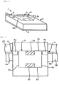
- Fig. 1 shows a perspective view for illustrating a dual mode band pass filter according to a first preferred embodiment of the invention.
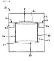
- Fig. 2 shows a plan view for schematically illustrating the main portion of the dual mode band pass filter.
- a dual mode band pass filter 1 includes a dielectric body 2 having a substantially rectangular planar configuration. On a top surface of the dielectric body 2 there is disposed a metal film 3 preferably made of Cu to define a resonator. The metal film 3 is partially provided on the dielectric body 3.
- the metal film 3 preferably has a substantially rectangular shape, in this preferred embodiment. That is, the shape of the metal film 3 includes widthwise and lengthwise directions.
- the metal film 3 is about 1.6 mm wide and about 1.4 mm long.
- the dimensions of the metal film 3 are not restricted to those described above. According to desired central frequencies and bandwidths, the dimensions can be changed appropriately.
- the input/output coupling circuits 5 and 6 include input/output capacitance generating patterns 5a and 6a as portions coupled to the metal film 3 via capacitances.
- the input/output capacitance generating patterns 5a and 6a are connected to microstrip lines 5b and 6b as external lines disposed on a dielectric mother body 110 via side surface electrodes disposed on side surfaces of the dielectric body 2 and via-hole electrodes disposed inside the dielectric body 2.
- the side surface electrodes and the via-hole electrodes are not shown in the figure.
- a ground electrode 4 is provided on an almost entire bottom surface of the dielectric body 2.
- the dielectric body 2 is not uniform, since there are some portions having relative permittivities different from that of the remaining portions of the dielectric body 2.
- each of the portions 2a and 2b has a relative permittivity ⁇ r of about 17 and the remaining portion of the dielectric body 2 has a relative permittivity ⁇ r of about 7.
- the portions 2a and 2b having the relatively high permittivities are disposed along widthwise sides 3c and 3d of the substantially rectangular metal film 3 near the center of each of the widthwise sides 3c and 3d.
- each of the portions 2a and 2b has a substantially rectangular planer shape, and is extended from the top surface of the dielectric body 2 to the bottom surface thereof in the thickness directions of the dielectric body 2.
- the dielectric body 2 including the portions 2a and 2b having permittivities higher than that of the remaining portion thereof.
- through-holes are made in areas for forming portions 2a and 2b and each of the through-holes is filled with a dielectric material having a relatively high permittivity.
- an element that reacts with a composite material of the dielectric body to cause heat diffusion so as to form the portions 2a and 2b.
- the dielectric body 2 is preferably made of an oxide such as Mg, Si, or Al.
- another oxide such as Ca or Ti is added to the portions 2a and 2b having relatively high permittivities.
- each of the portions 2a and 2b having relatively high permittivities preferably has a substantially rectangular planer shape, which is, for example, approximately 200 ⁇ m long and approximately 600 ⁇ m wide.
- an input voltage is applied between one of the input/output coupling circuits 5 and 6 and the ground electrode 4 to extract an output voltage between the ground electrode 4 and the remaining one of the input/output coupling circuits 5 and 6.
- the metal film 3 is substantially rectangular and there are provided the portions 2a and 2b have relatively high permittivities, two resonance modes are coupled to each other to allow the filter to function as a dual mode band pass filter. This is because the portions 2a and 2b have relatively high permittivities are arranged such that the two resonance modes generated at the metal film 3 are mutually coupled. This will be illustrated below with reference to Figs. 3 to 7.
- Fig. 3 shows a perspective view of a filter 51 prepared for comparison to preferred embodiments of the present invention.
- the filter 51 has an arrangement that is the same as that of the dual mode band pass filter 1 of the present preferred embodiment, except that there are no portions 2a and 2b having relatively high permittivities.
- Fig. 4 shows the frequency characteristics of the filter 51.
- a solid line A and a broken line B indicate the reflection characteristics and passing characteristics of the filter 51.
- a resonance mode indicated by the arrow C which is hereinafter referred to as a resonance mode C
- a resonance mode indicated by the arrow D is the resonance mode along the lengthwise direction.
- the filter 51 does not function as a dual mode band pass filter.
- the inventors of the present invention measured resonance electric fields generated on the resonator of the filter 51 by using an electromagnetic field simulator (Hewlett-Packard Co., No. HFSS) and obtained the following results, which will be shown in Figs. 5 and 6.
- a dual mode band pass filter could be formed by adjusting the resonance electric fields generated in one of the two resonance modes C and D to make the resonance frequencies of the resonance modes C and D closer to each other.
- the portions 2a and 2b having the relatively high permittivities are provided at substantially central portions of the widthwise sides 3c and 3d.
- the resonance frequency of the resonance mode along each of the lengthwise sides that is, the resonance frequency of the resonance mode D shown in Fig. 4 is reduced, and the two resonance modes are thereby mutually coupled.
- the portions 2a and 2b having the relatively high permittivities are arranged such that the two resonance modes are mutually coupled.
- Fig. 7 shows the frequency characteristics of the dual mode band pass filter 1 of the first preferred embodiment of the present invention.
- a solid line G indicates the reflection characteristics of the filter 1
- a broken line H indicates the passing characteristics of the filter 1.
- the frequency characteristics of the filter 51 shown above are also indicated by a solid line A and a broken line B.
- the filter 1 functions as a dual mode band pass filter.
- the difference between the relative permittivity of each of the portions 2a and 2b and the relative permittivity of the remaining portions, the planar shapes of the portions 2a and 2b, and the area dimensions of the planar shapes thereof are adjusted to facilitate adjustments of the frequency of the resonance mode propagating in each of the lengthwise directions.
- the portions 2a and 2b having relatively high permittivities are arranged in the approximately central portions of the widthwise sides.
- the portions having relative permittivities different from that of the remaining portion may be disposed at the lengthwise sides. In this case, this arrangement influences the frequency of a resonance mode propagating along each of the widthwise sides.
- portions having relative permittivities different from that of the remaining portion it is necessary to provide portions having relative permittivities that are lower than that of the remaining portion at the lengthwise sides.
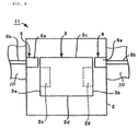
- Fig. 8 shows a schematic plan view of a modified example of the band pass filter 1, in which portions having relatively low permittivities are disposed at lengthwise sides 3a and 3b of a metal film 3.
- cavities 2c and 2d are provided in a dielectric body 2.
- the cavities 2c and 2d are disposed substantially in the approximate center of each of the lengthwise sides 3a and 3b in such a manner that the cavities 2c and 2d are positioned along the lengthwise sides 3a and 3b in a region where the metal film 3 is opposed to a ground electrode.
- Each of the cavities 2c and 2d has a substantially rectangular planar shape, which is, for example, approximately 200 ⁇ m long and approximately 600 ⁇ m wide.
- the cavities 2c and 2d penetrate from a top surface of the dielectric body 2 to a bottom surface thereof. However, it is not always necessary to form the cavities 2c and 2d in such a penetrating manner.
- the relative permittivity of each of the cavities 2c and 2d is substantially equivalent to a relative permittivity of air. That is, the relative permittivity ⁇ r is equal to 1.
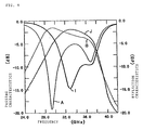
- Fig. 9 shows the frequency characteristics of the dual mode band pass filter 11 according to the modified example.
- a solid line I indicates the reflection characteristics of the filter 11 and a broken line J indicates passing characteristics thereof.
- the frequency characteristics of the filter 51 described above are also indicated by a solid line A and a broken line B.
- the filter 11 As shown in Fig. 9, in the filter 11 according to the modified example, at the lengthwise sides of the metal film 3, the cavities 2c and 2d are disposed in the dielectric body 2. As a result, this arrangement influences the resonance electric field of a resonance mode propagating in each of the widthwise directions of the metal film 3. As a result, since the frequency of the resonance mode C becomes higher and the two resonance modes are thereby mutually coupled, the filter 11 functions as a dual mode band pass filter.
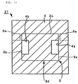
- Fig. 10 shows a schematic plan view of the main portion of a band pass filter according to a second preferred embodiment of the present invention.
- Fig. 11 shows a bottom surface view thereof.
- a dielectric body 22 preferably has a thickness of about 300 ⁇ m, and is preferably made of an oxide Mg, Si, or Al having a relative permittivity ⁇ r 7.
- a metal film 3 and input/output coupling circuits 5 and 6 are arranged in the same way as those of the first preferred embodiment of the present invention.
- a ground electrode 4 is disposed on a bottom surface of the dielectric body 22.
- openings 4a and 4b are provided in the ground electrode 4.
- the openings 4a and 4b are arranged to couple two resonance modes in a region where the metal film 3 is opposed to the ground electrode 4.
- the openings 4a and 4b have substantially rectangular planar shapes in such a manner that the openings 4a and 4b are positioned along the lengthwise sides 3a and 3b of an image of the metal film 3 downwardly projected.
- the openings 4a and 4b influence portions at which the resonance electric fields of resonance modes propagating in the widthwise sides of the metal film 3 are intensively generated.
- the resonance frequency of the resonance mode C propagating in each of the widthwise directions of the metal film 3 becomes higher.
- the dimensions of the openings 4a and 4b are arranged such that the resonance modes C and D are mutually coupled.
- the widthwise sides of each of the openings 4a and 4b are about 0.8 mm long and the lengthwise sides of thereof are about 0.4 mm long.
- a solid line K and a broken line L shown in Fig. 12 indicate the frequency characteristics of the dual mode band pass filter 21 of the second preferred embodiment.
- the solid line K indicates the reflection characteristics of the filter 21 and the broken line L indicates the passing characteristics thereof.
- the frequency characteristics of the filter 51 described above are also shown in Fig. 12.
- two resonance modes are coupled to each other by forming the openings 4a and 4b.
- the portions having relative permittivities different from that of the remaining potion are provided on the dielectric body, and in the second preferred embodiment, the openings are disposed in the ground electrode in order to control the resonance electric fields.
- these methods may be used together. That is, both methods of the first preferred embodiment and the second preferred embodiment may be combined.
- the metal film 3 preferably has a substantially rectangular shape in each of the first and second preferred embodiments, the shape of the metal film 3 is not restricted to that and it can be arbitrary. Nevertheless, in order to generate two resonance modes having different resonance frequencies, it is preferable to use a metal film having widthwise directions and lengthwise directions.
- planar shape of the metal film may be various shapes including substantially rectangular, substantially rhombic, substantially polygonal, substantially circular, or substantially elliptical.
- the metal film 3 may be formed on the top surface of the dielectric body 2, the metal film 3 may be disposed at a certain height in the dielectric body.
- the ground electrode 4 may be provided inside the dielectric body 2.
- a dual mode band pass filter having a triplate structure may be provided by disposing the metal film at the intermediate height position of the dielectric body 2 and disposing the ground electrode on a top surface and a bottom surface of the dielectric body 2.
- a metal film for forming a resonator is disposed on a dielectric body, and there are provided input/output coupling circuits coupled to the metal film so that two resonance modes are generated.
- the relative permittivities of portions of the dielectric body are made different from a relative permittivity of the remaining portion of the dielectric body in a region where the metal film is opposed to the ground electrode via the dielectric body.
- the shape of the metal film defining the resonator and the positions of points for coupling the input/output coupling circuits to the metal film are restricted.
- the dual mode band pass filter of preferred embodiments of the present invention does not have any such restrictions.
- a dual mode band pass filter can be more freely designed.
- wider adjustments of the bandwidth of the filter can be made by changing the dimensions of the metal film, the dimensions of the portions of the dielectric body having relative permittivities different from that of the remaining portion thereof, and the positions of the coupling points of the input/output coupling circuits.
- the portions having the different relative permittivities are provided by the cavities disposed in the dielectric body, by only forming the cavities in the dielectric body, the two resonance modes can be easily coupled to each other.
- a metal film for forming a resonator is disposed on the dielectric body. Since the metal film is coupled to the input/output coupling circuits, two resonance modes are generated. In order to couple the two resonance modes, potions of a ground electrode are cut away in a region where the metal film is opposed to the ground electrode. As a result, similar to the first preferred embodiment of the invention, since the two resonance modes are mutually coupled, the characteristics of a dual mode band pass filter can be obtained.
- the dual mode band pass filter can be more freely designed.
- wider adjustments of the bandwidth can be made by changing the shapes of the openings or cut-away portions disposed in the ground electrode, the positions of the coupling points of the input/output coupling circuits, and the dimensions of the metal film.
- the dual mode band pass filter having a desired bandwidth can be easily obtained.
- the dual mode band pass filter according to preferred embodiments of the present invention can be easily obtained.
- the metal film has a shape that includes widthwise and lengthwise dimensions, the two resonance modes having different resonance frequencies can be easily generated.
- planar shape of the metal film is not restricted to a specific one, a metal film having a variety of shapes can be used in each of the dual mode band pass filters of the first and second preferred embodiments of the present invention.
- the planar shape of the metal film may be substantially rectangular, substantially rhombic, substantially polygonal, substantially circular, or substantially elliptical.
Landscapes
- Physics & Mathematics (AREA)
- Electromagnetism (AREA)
- Control Of Motors That Do Not Use Commutators (AREA)
Priority Applications (1)
| Application Number | Priority Date | Filing Date | Title |
|---|---|---|---|
| EP03019351A EP1396904A3 (de) | 2000-05-23 | 2001-05-08 | Dualmode Bandpassfilter |
Applications Claiming Priority (2)
| Application Number | Priority Date | Filing Date | Title |
|---|---|---|---|
| JP2000151756A JP3562442B2 (ja) | 2000-05-23 | 2000-05-23 | デュアルモード・バンドパスフィルタ |
| JP2000151756 | 2000-05-23 |
Related Child Applications (1)
| Application Number | Title | Priority Date | Filing Date |
|---|---|---|---|
| EP03019351A Division EP1396904A3 (de) | 2000-05-23 | 2001-05-08 | Dualmode Bandpassfilter |
Publications (3)
| Publication Number | Publication Date |
|---|---|
| EP1170819A2 true EP1170819A2 (de) | 2002-01-09 |
| EP1170819A3 EP1170819A3 (de) | 2002-01-16 |
| EP1170819B1 EP1170819B1 (de) | 2005-02-23 |
Family
ID=18657260
Family Applications (2)
| Application Number | Title | Priority Date | Filing Date |
|---|---|---|---|
| EP03019351A Withdrawn EP1396904A3 (de) | 2000-05-23 | 2001-05-08 | Dualmode Bandpassfilter |
| EP01111072A Expired - Lifetime EP1170819B1 (de) | 2000-05-23 | 2001-05-08 | Dualmode Bandpassfilter |
Family Applications Before (1)
| Application Number | Title | Priority Date | Filing Date |
|---|---|---|---|
| EP03019351A Withdrawn EP1396904A3 (de) | 2000-05-23 | 2001-05-08 | Dualmode Bandpassfilter |
Country Status (5)
| Country | Link |
|---|---|
| US (1) | US6556109B2 (de) |
| EP (2) | EP1396904A3 (de) |
| JP (1) | JP3562442B2 (de) |
| KR (1) | KR100397733B1 (de) |
| DE (1) | DE60109001T2 (de) |
Families Citing this family (9)
| Publication number | Priority date | Publication date | Assignee | Title |
|---|---|---|---|---|
| EP1223591A3 (de) * | 2001-01-11 | 2007-06-06 | Matsushita Electric Industrial Co., Ltd. | Vielschichtelektronikbauteil und Kommunikationsgerät |
| US6825740B2 (en) * | 2002-02-08 | 2004-11-30 | Tdk Corporation | TEM dual-mode rectangular dielectric waveguide bandpass filter |
| US6963259B2 (en) * | 2002-06-27 | 2005-11-08 | Harris Corporation | High efficiency resonant line |
| US6727785B2 (en) * | 2002-06-27 | 2004-04-27 | Harris Corporation | High efficiency single port resonant line |
| US6903634B2 (en) * | 2002-11-12 | 2005-06-07 | Silicon Integrated Systems Corp. | Method of detuning resonant frequencies of a power distribution system |
| JP5029519B2 (ja) * | 2008-07-08 | 2012-09-19 | 富士通株式会社 | フィルタ |
| TWI381574B (zh) * | 2008-09-24 | 2013-01-01 | Univ Nat Changhua Education | Dual band bandpass filter |
| JP5120278B2 (ja) * | 2009-01-26 | 2013-01-16 | 富士通株式会社 | 超伝導チューナブルフィルタ装置、非線形歪測定装置、非線形歪測定方法 |
| US9490768B2 (en) * | 2012-06-25 | 2016-11-08 | Knowles Cazenovia Inc. | High frequency band pass filter with coupled surface mount transition |
Family Cites Families (12)
| Publication number | Priority date | Publication date | Assignee | Title |
|---|---|---|---|---|
| US4488131A (en) * | 1983-02-25 | 1984-12-11 | Hughes Aircraft Company | MIC Dual mode ring resonator filter |
| US5136268A (en) * | 1991-04-19 | 1992-08-04 | Space Systems/Loral, Inc. | Miniature dual mode planar filters |
| JP2906863B2 (ja) | 1992-09-28 | 1999-06-21 | 松下電器産業株式会社 | ストリップ線路デュアル・モード・フィルタ |
| WO1995028746A2 (en) * | 1994-04-14 | 1995-10-26 | E.I. Du Pont De Nemours And Company | High power high-temperature superconductive filters |
| GB9426294D0 (en) * | 1994-12-28 | 1995-02-22 | Mansour Raafat | High power soperconductive circuits and method of construction thereof |
| JPH08204437A (ja) * | 1995-01-30 | 1996-08-09 | Matsushita Electric Works Ltd | マイクロストリップアンテナの共振周波数調整方法 |
| US5750473A (en) * | 1995-05-11 | 1998-05-12 | E. I. Du Pont De Nemours And Company | Planar high temperature superconductor filters with backside coupling |
| JP3304724B2 (ja) | 1995-11-16 | 2002-07-22 | 松下電器産業株式会社 | デュアルモードフィルタ |
| JPH09162610A (ja) | 1995-12-14 | 1997-06-20 | Matsushita Electric Ind Co Ltd | デュアルモード共振器 |
| US5751201A (en) * | 1996-06-19 | 1998-05-12 | Motorola, Inc. | Resonator with metal layers devoid of DC connection and semiconductor device in substrate |
| JP3277834B2 (ja) * | 1996-12-11 | 2002-04-22 | 松下電器産業株式会社 | 平面バンドパスフィルタ |
| JPH11122032A (ja) * | 1997-10-11 | 1999-04-30 | Yokowo Co Ltd | マイクロストリップアンテナ |
-
2000
- 2000-05-23 JP JP2000151756A patent/JP3562442B2/ja not_active Expired - Fee Related
-
2001
- 2001-05-08 EP EP03019351A patent/EP1396904A3/de not_active Withdrawn
- 2001-05-08 EP EP01111072A patent/EP1170819B1/de not_active Expired - Lifetime
- 2001-05-08 DE DE60109001T patent/DE60109001T2/de not_active Expired - Lifetime
- 2001-05-15 US US09/855,298 patent/US6556109B2/en not_active Expired - Fee Related
- 2001-05-23 KR KR10-2001-0028464A patent/KR100397733B1/ko not_active Expired - Fee Related
Also Published As
| Publication number | Publication date |
|---|---|
| KR100397733B1 (ko) | 2003-09-13 |
| EP1396904A2 (de) | 2004-03-10 |
| DE60109001T2 (de) | 2006-02-09 |
| JP3562442B2 (ja) | 2004-09-08 |
| EP1170819A3 (de) | 2002-01-16 |
| DE60109001D1 (de) | 2005-03-31 |
| JP2001332905A (ja) | 2001-11-30 |
| EP1170819B1 (de) | 2005-02-23 |
| EP1396904A3 (de) | 2005-11-30 |
| US20020039059A1 (en) | 2002-04-04 |
| US6556109B2 (en) | 2003-04-29 |
| KR20010107691A (ko) | 2001-12-07 |
Similar Documents
| Publication | Publication Date | Title |
|---|---|---|
| EP1128460B1 (de) | Zweifachmodus-Bandpassfilter | |
| JP2001077609A (ja) | 誘電体共振器、インダクタ、キャパシタ、誘電体フィルタ、発振器、誘電体デュプレクサおよび通信装置 | |
| EP1170819B1 (de) | Dualmode Bandpassfilter | |
| US6812813B2 (en) | Method for adjusting frequency of attenuation pole of dual-mode band pass filter | |
| US6630875B2 (en) | Dual-mode band-pass filter | |
| US7274273B2 (en) | Dielectric resonator device, dielectric filter, duplexer, and high-frequency communication apparatus | |
| JP2004320351A (ja) | デュアルモード・バンドパスフィルタ、デュプレクサ及び無線通信装置 | |
| JP4438253B2 (ja) | バンドパスフィルタの特性調整方法 | |
| JP4442066B2 (ja) | デュアルモード・バンドパスフィルタ及びデュアルモード・バンドパスフィルタの特性調整方法並びにデュプレクサ及び無線通信装置 | |
| US7183874B2 (en) | Casing contained filter | |
| JP2002261508A (ja) | デュアルモード・バンドパスフィルタ並びにデュプレクサ及び無線通信装置 | |
| JP2002237701A (ja) | 導波管型誘電体フィルタ | |
| JP2000134004A (ja) | 誘電体フィルタ | |
| JP2004312184A (ja) | デュアルモード・バンドパスフィルタ、デュプレクサ及び無線通信装置 |
Legal Events
| Date | Code | Title | Description |
|---|---|---|---|
| PUAI | Public reference made under article 153(3) epc to a published international application that has entered the european phase |
Free format text: ORIGINAL CODE: 0009012 |
|
| PUAL | Search report despatched |
Free format text: ORIGINAL CODE: 0009013 |
|
| 17P | Request for examination filed |
Effective date: 20010508 |
|
| AK | Designated contracting states |
Kind code of ref document: A2 Designated state(s): AT BE CH CY DE DK ES FI FR GB GR IE IT LI LU MC NL PT SE TR Kind code of ref document: A2 Designated state(s): DE FR GB |
|
| AX | Request for extension of the european patent |
Free format text: AL;LT;LV;MK;RO;SI |
|
| AK | Designated contracting states |
Kind code of ref document: A3 Designated state(s): AT BE CH CY DE DK ES FI FR GB GR IE IT LI LU MC NL PT SE TR |
|
| AX | Request for extension of the european patent |
Free format text: AL;LT;LV;MK;RO;SI |
|
| AKX | Designation fees paid |
Free format text: DE FR GB |
|
| 17Q | First examination report despatched |
Effective date: 20030218 |
|
| GRAP | Despatch of communication of intention to grant a patent |
Free format text: ORIGINAL CODE: EPIDOSNIGR1 |
|
| GRAS | Grant fee paid |
Free format text: ORIGINAL CODE: EPIDOSNIGR3 |
|
| GRAA | (expected) grant |
Free format text: ORIGINAL CODE: 0009210 |
|
| AK | Designated contracting states |
Kind code of ref document: B1 Designated state(s): DE FR GB |
|
| REG | Reference to a national code |
Ref country code: GB Ref legal event code: FG4D |
|
| REG | Reference to a national code |
Ref country code: IE Ref legal event code: FG4D |
|
| REF | Corresponds to: |
Ref document number: 60109001 Country of ref document: DE Date of ref document: 20050331 Kind code of ref document: P |
|
| PLBE | No opposition filed within time limit |
Free format text: ORIGINAL CODE: 0009261 |
|
| STAA | Information on the status of an ep patent application or granted ep patent |
Free format text: STATUS: NO OPPOSITION FILED WITHIN TIME LIMIT |
|
| 26N | No opposition filed |
Effective date: 20051124 |
|
| ET | Fr: translation filed | ||
| PGFP | Annual fee paid to national office [announced via postgrant information from national office to epo] |
Ref country code: DE Payment date: 20120502 Year of fee payment: 12 |
|
| PGFP | Annual fee paid to national office [announced via postgrant information from national office to epo] |
Ref country code: GB Payment date: 20120502 Year of fee payment: 12 Ref country code: FR Payment date: 20120608 Year of fee payment: 12 |
|
| GBPC | Gb: european patent ceased through non-payment of renewal fee |
Effective date: 20130508 |
|
| PG25 | Lapsed in a contracting state [announced via postgrant information from national office to epo] |
Ref country code: DE Free format text: LAPSE BECAUSE OF NON-PAYMENT OF DUE FEES Effective date: 20131203 |
|
| REG | Reference to a national code |
Ref country code: DE Ref legal event code: R119 Ref document number: 60109001 Country of ref document: DE Effective date: 20131203 |
|
| REG | Reference to a national code |
Ref country code: FR Ref legal event code: ST Effective date: 20140131 |
|
| PG25 | Lapsed in a contracting state [announced via postgrant information from national office to epo] |
Ref country code: GB Free format text: LAPSE BECAUSE OF NON-PAYMENT OF DUE FEES Effective date: 20130508 |
|
| PG25 | Lapsed in a contracting state [announced via postgrant information from national office to epo] |
Ref country code: FR Free format text: LAPSE BECAUSE OF NON-PAYMENT OF DUE FEES Effective date: 20130531 |