EP1170841A2 - Optische Halbleitervorrichtung und zugehöriges Herstellungsverfahren - Google Patents
Optische Halbleitervorrichtung und zugehöriges Herstellungsverfahren Download PDFInfo
- Publication number
- EP1170841A2 EP1170841A2 EP01116355A EP01116355A EP1170841A2 EP 1170841 A2 EP1170841 A2 EP 1170841A2 EP 01116355 A EP01116355 A EP 01116355A EP 01116355 A EP01116355 A EP 01116355A EP 1170841 A2 EP1170841 A2 EP 1170841A2
- Authority
- EP
- European Patent Office
- Prior art keywords
- optical
- semiconductor device
- optical semiconductor
- group
- vapor phase
- Prior art date
- Legal status (The legal status is an assumption and is not a legal conclusion. Google has not performed a legal analysis and makes no representation as to the accuracy of the status listed.)
- Withdrawn
Links
Images






Classifications
-
- H—ELECTRICITY
- H10—SEMICONDUCTOR DEVICES; ELECTRIC SOLID-STATE DEVICES NOT OTHERWISE PROVIDED FOR
- H10H—INORGANIC LIGHT-EMITTING SEMICONDUCTOR DEVICES HAVING POTENTIAL BARRIERS
- H10H29/00—Integrated devices, or assemblies of multiple devices, comprising at least one light-emitting semiconductor element covered by group H10H20/00
- H10H29/10—Integrated devices comprising at least one light-emitting semiconductor component covered by group H10H20/00
-
- H—ELECTRICITY
- H01—ELECTRIC ELEMENTS
- H01S—DEVICES USING THE PROCESS OF LIGHT AMPLIFICATION BY STIMULATED EMISSION OF RADIATION [LASER] TO AMPLIFY OR GENERATE LIGHT; DEVICES USING STIMULATED EMISSION OF ELECTROMAGNETIC RADIATION IN WAVE RANGES OTHER THAN OPTICAL
- H01S5/00—Semiconductor lasers
- H01S5/02—Structural details or components not essential to laser action
- H01S5/026—Monolithically integrated components, e.g. waveguides, monitoring photo-detectors, drivers
- H01S5/0265—Intensity modulators
-
- H—ELECTRICITY
- H01—ELECTRIC ELEMENTS
- H01S—DEVICES USING THE PROCESS OF LIGHT AMPLIFICATION BY STIMULATED EMISSION OF RADIATION [LASER] TO AMPLIFY OR GENERATE LIGHT; DEVICES USING STIMULATED EMISSION OF ELECTROMAGNETIC RADIATION IN WAVE RANGES OTHER THAN OPTICAL
- H01S5/00—Semiconductor lasers
- H01S5/20—Structure or shape of the semiconductor body to guide the optical wave ; Confining structures perpendicular to the optical axis, e.g. index or gain guiding, stripe geometry, broad area lasers, gain tailoring, transverse or lateral reflectors, special cladding structures, MQW barrier reflection layers
- H01S5/2054—Methods of obtaining the confinement
- H01S5/2077—Methods of obtaining the confinement using lateral bandgap control during growth, e.g. selective growth, mask induced
-
- H—ELECTRICITY
- H01—ELECTRIC ELEMENTS
- H01S—DEVICES USING THE PROCESS OF LIGHT AMPLIFICATION BY STIMULATED EMISSION OF RADIATION [LASER] TO AMPLIFY OR GENERATE LIGHT; DEVICES USING STIMULATED EMISSION OF ELECTROMAGNETIC RADIATION IN WAVE RANGES OTHER THAN OPTICAL
- H01S5/00—Semiconductor lasers
- H01S5/20—Structure or shape of the semiconductor body to guide the optical wave ; Confining structures perpendicular to the optical axis, e.g. index or gain guiding, stripe geometry, broad area lasers, gain tailoring, transverse or lateral reflectors, special cladding structures, MQW barrier reflection layers
- H01S5/22—Structure or shape of the semiconductor body to guide the optical wave ; Confining structures perpendicular to the optical axis, e.g. index or gain guiding, stripe geometry, broad area lasers, gain tailoring, transverse or lateral reflectors, special cladding structures, MQW barrier reflection layers having a ridge or stripe structure
- H01S5/227—Buried mesa structure ; Striped active layer
- H01S5/2272—Buried mesa structure ; Striped active layer grown by a mask induced selective growth
Definitions
- the present invention relates to an optical semiconductor device and a method for manufacturing the same, and a technology preferably applied to an optical module and an optical communication apparatus provided with the optical semiconductor device.
- Semiconductor lasers and semiconductor optical modulators are key devices which support optical fiber communications systems, and are strongly required to have a higher performance, more advanced functions, and a lower cost as technology advances to meet the rapidly growing demands for telecommunication.
- DFB-LD distributed feedback laser diodes
- external optical modulators play important roles as the source and processor of optical signals.
- monolithic integration of these devices has made it possible to reduce the size, power consumption, and cost of the device.
- the integrated device which is called an DFB-LD integrated with electro-absorption type modulator (DFB/MOD)
- DFB/MOD electro-absorption type modulator
- MOVPE selective metal-organic vapor phase epitaxy
- a spot-size converter integrated laser diode which operates over a broad range of temperatures and which has a semiconductor laser that performs the functions of a lens, is viewed as the key device for providing a module incorporating the semiconductor laser as the light source without using a temperature regulator and lenses.
- Manufacture of the SSC-LD also employs in-plane band gap control technology and film thickness control technology based on the selective MOVPE process.
- the band gap wavelength and film thickness can be changed in the wafer surface by the selective MOVPE process through a mechanism as described below.
- the film thickness (growth rate) is changed by selective growth.
- the first reason is as follows. Since the material of group III elements, which has reached a dielectric mask provided on the surface of the semiconductor substrate in order to carry out selective growth, is not deposited on the dielectric material (crystal growth does not occur), the particles of these elements migrate over the mask surface to reach the growth region. Consequently, as the mask width increases, the amount of the group III element material which migrates increases, thereby increasing the growth rate of the selective growth region.
- the distance of migration and the probability of being captured in the selective growth region are different among the different group III elements, and therefore the band gap wavelength varies as the proportions of the group III elements (proportions of In and Ga in the case of InGaAsP) in the selective growth region change.
- the second reason is as follows. Since the group III element material which has reached the dielectric mask is not deposited on the dielectric material (crystal growth does not occur) as described above, the concentration of the element in the vapor phase on the dielectric mask increases while the particles of the element are consumed in growing the crystal in the selective growth region, thus resulting in decreasing the concentration of the element in the vapor phase. As a result, vapor phase diffusion occurs because the concentration of the element has a graded distribution in the lateral direction parallel to the substrate in the vapor phase, thus leading to a flow of the source materials of the element from the dielectric mask region into the selective growth region.
- the rate of crystal growth increases with the width of the dielectric mask.
- the distance of migration in the vapor phase diffusion and the probability of being captured in the selective growth region are different among the different group III elements, and therefore the band gap wavelength varies as the proportions of the group III elements (proportions of In and Ga in the case of InGaAsP) change in the selective growth region.
- the present invention has been made in light of the problems described above, and an object thereof is to provide a means for matching both the band gap wavelength and the lattice constant to the design values by controlling the proportions of the group V elements to desired values when manufacturing a compound semiconductor which includes two or more kinds of group V elements, such as InGaAsP, by the selective MOVPE process.
- Another object of the present invention is to improve the characteristics of a semiconductor optical device constituted mainly from a compound semiconductor which includes at least two kinds of group V elements, such as InGaAsP, by the selective MOVPE process.
- the optical semiconductor device and the method for manufacturing the same according to the present invention aim at providing a means for improving the characteristics of the semiconductor optical device formed by the selective MOVPE process, namely achieving a crystal of high quality grown by the selective MOVPE process by making corrections for the change in the proportions of the group V elements which has been ignored in the prior art.
- the present invention provides an optical semiconductor device constituted mainly from a III-V compound semiconductor crystal grown by the selective metal-organic vapor phase epitaxy process which includes at least two kinds of group V elements, and achieves the objects described above by forming the III-V compound semiconductor under the conditions of supplying group V element materials different from those of the non-selective metal-organic vapor phase epitaxy process in order for the compound semiconductor to include the group V elements in the desired proportions.
- the III-V compound semiconductor crystal grown by the selective metal-organic vapor phase epitaxy process preferably has an optical waveguide structure.
- the III-V compound semiconductor crystal grown by the selective metal-organic vapor phase epitaxy process may be used as an active layer of a semiconductor laser.
- the III-V compound semiconductor grown by the selective metal-organic vapor phase epitaxy process is used as a light absorption layer of a semiconductor optical modulator.
- the III-V compound semiconductor grown by the selective metal-organic vapor phase epitaxy process is used as a light absorption layer of a semiconductor laser optical detector.
- the III-V compound semiconductor grown by the selective metal-organic vapor phase epitaxy process is used as a core layer of a semiconductor optical multiplexer/demultiplexer.
- the III-V compound semiconductor grown by the selective metal-organic vapor phase epitaxy process is used as a core layer of a semiconductor optical switch.
- the optical semiconductor device of the present invention may be constituted by integrating at least two kinds of the optical semiconductor device comprising the III-V compound semiconductor grown by the selective metal-organic vapor phase epitaxy process as the components thereof.
- the method of the present invention for manufacturing the optical semiconductor device comprising the III-V compound semiconductor which includes two or more kinds of group V elements is based on the selective metal-organic vapor phase epitaxy process, and the amounts of the group V element materials supplied are controlled to desired values based on a correction of the conditions of the non-selective metal-organic vapor phase epitaxy process in order to achieve the desired proportions of the group V elements in the selective growth region, thereby solving the problems described above.
- the method of the present invention for manufacturing the optical semiconductor device comprising the III-V compound semiconductor which includes two or more kinds of group III elements and two or more kinds of group V elements is based on the selective metal-organic vapor phase epitaxy process, wherein the amounts of the group III element materials and the group V element materials supplied are corrected according to the conditions of the non-selective metal-organic vapor phase epitaxy process in order to control the band gap energy and the proportions of the group V elements in the selective growth region to desired values, thereby solving the problems described above.
- the selective metal-organic vapor phase epitaxy process may be a narrow-width selective metal-organic vapor phase epitaxy process which is capable of directly forming a semiconductor optical waveguide.
- the amount of correction from the conditions of the selective metal-organic vapor phase epitaxy process can be determined so that the peak intensity of the photoluminescence spectrum that determines the band gap wavelength becomes a maximum, while changing the amounts of the group III element materials and the group V element materials being supplied at the same time under conditions such that the band gap wavelength remains constant.
- the amount of correction from the conditions of the selective metal-organic vapor phase epitaxy process can be determined so that the half-width of the photoluminescence spectrum that determines the band gap wavelength becomes a minimum, while changing the amounts of the group III element materials and the group V element materials being supplied at the same time under conditions such that the band gap wavelength remains constant.
- the III-V compound semiconductor may include at least one element selected from among indium, gallium, aluminum, and thallium as the group III element and at least two elements selected from among phosphorus, arsenic, nitrogen, and antimony as the group V elements.
- the III-V compound semiconductor may specifically be InGaAsP.
- the optical module comprises the optical semiconductor device described above or an optical semiconductor device manufactured by the manufacturing method of the present invention, a means for extracting the optical output from the optical semiconductor device, a mechanism for sending the optical output from the optical semiconductor device to the extracting means, and an electric interface for driving the optical semiconductor device, thereby achieving the objects described above.
- the optical module may comprise the optical semiconductor device described above or an optical semiconductor device manufactured by the manufacturing method of the present invention, a means for extracting the optical output light to the optical semiconductor device from the outside, a mechanism for sending the optical output to the optical semiconductor device from the extracting means, and an electric interface for driving the optical semiconductor device.
- the present invention provides an optical communication apparatus comprising the optical semiconductor device described above or an optical semiconductor device manufactured by the manufacturing method of the present invention, or the optical module and a receiving apparatus for receiving the optical output from an optical transmitter, thereby achieving the objects described above.
- the optical communication apparatus may comprise an optical receiver which has the optical semiconductor device described above or an optical semiconductor device manufactured by the manufacturing method of the present invention, or the optical module installed therein and a transmitter for transmitting the optical input to the optical receiver.
- FIG. 1 is a schematic sectional view showing the optical semiconductor device having the composition of InP/InGaAsP/InP formed by the selective MOVPE growing process, wherein reference symbol 1 denotes a (100) InP substrate and 2 denotes an SiO 2 stripe mask.
- the InP/InGaAsP/InP structure is selectively grown by the selective MOVPE growing process wherein an InP layer 3a, an InGaAsP layer 3b, and an InP layer 3c are stacked by using the stripe mask 2 constituted from a pair of dielectric films (SiO 2 ) formed on the (100) InP substrate 1 at a 1.5 ⁇ m interval in the [011] direction.
- the stripe mask 2 constituted from a pair of dielectric films (SiO 2 ) formed on the (100) InP substrate 1 at a 1.5 ⁇ m interval in the [011] direction.
- the selective MOVPE growing process is carried out under conditions of an oversupply of a group V element material where the group V element material has a very low adhesion coefficient which means there is no gradient in the concentration distribution of the group V element between the selective growth region and the dielectric mask forming region, it has been believed that the flow of the source materials of the group V element from the dielectric mask region into the selective growth region does not occur, and therefore the proportion of the group V element does not change.
- the microscopic PL method was carried out by using an argon ion laser oscillating at a wavelength of 514.5 nm as the excitation light source with the beam regulated to have a diameter of 1 ⁇ m.
- micro X-ray diffraction analysis was carried out by using a micro X-ray beam regulated so as to have a diameter of 5 ⁇ m, which was generated from synchrotron radiation light (SR light) of 15 keV in energy and 0.0827 nm in the X-ray wavelength.
- SR light synchrotron radiation light
- FIG. 2 shows the relationship between the band gap wavelength of the selectively grown InGaAsP layer 3b measured by the microscopic photoluminescence (PL) method and the width of the SiO 2 mask.
- the PL peak wavelength which corresponds to the band gap wavelength is plotted along the ordinate and the SiO 2 mask width is plotted along the abscissa.
- the PL peak wavelength (band gap wavelength) becomes longer as the mask width increases. This has previously been interpreted as the result of compressive strain being introduced by the increase in the proportion of In which is a group III element.
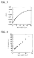
- the ratio ⁇ d/d represents the lattice strain
- the graph shows that the lattice constant increase, shifting toward the compressive strain side as the mask width increases.
- FIG. 4 shows the relationship of the mask width to the film thickness of the selectively grown InGaAsP layer 3b measured with a scanning electron microscope.
- the proportions of the constituent elements of InGaAsP can be uniquely determined when provided with the information of the band gap wavelength and the lattice constant, plus the film thickness for the case when a quantum effect is added to the band gap wavelength.
- FIG. 5 shows the mask width dependency of the proportion y of group V element As and the proportion x of group III element In for the case when the composition of InGaAsP is represented as In x Ga 1-x As y P 1-y (0 ⁇ x ⁇ 1, 0 ⁇ y ⁇ 1).
- the crystal growing conditions have been determined by estimating the lattice strain from only the PL peak wavelength and the film thickness shown in FIG. 2 and FIG. 4, thereby correcting the flow rate of the group III material based on the estimation.
- the estimated value of the lattice strain is different from the actual value of the lattice strain.
- the crystal growth conditions are set so as to achieve lattice matching of the InGaAsP 3b layer grown by the selective MOVPE process to the InP substrate by employing the amount of lattice strain calculated based on the conventional assumption, a tensile-strained crystal would result.
- the proportions of the constituents In, Ga, As, and P in InGaAsP can be uniquely determined from the two parameters of the band gap wavelength and the lattice constant, or three parameters including the film thickness added to the above, for the case when a quantum effect is added to the band gap wavelength.
- the X-ray diffraction analysis technique that uses a micro X-ray beam on a microscopic scale has not yet advanced to a stage such that can be easily used for determining the lattice constant in the selective growth region in the routine work.
- This method relies only on the microscopic PL measurement for setting the conditions of lattice matching in some area of an InP substrate with a desired mask width when forming InGaAsP by narrow-width selective growth.
- the thickness of the InGaAsP layer which is to be grown by the selective MOVPE process is several hundreds of nanometers or greater.
- the existence of a lattice mismatch exceeding a certain level causes dislocation in the crystal, non-radiative centers increase and the band gap energy fluctuates due to relaxation of the lattice strain.
- the PL measurement provides a decreasing PL light emission intensity and an increasing PL spectrum width.
- the lattice matching conditions can be determined with an accuracy of residual strain to within 0.1% so as to maximize the PL intensity or minimize the PL spectrum width in the selective MOVPE growth process to a film thickness of about 200 nm with a desired mask width.
- both the As/P ratio and In/Ga ratio are changed simultaneously under the conditions which maintain a constant band gap wavelength (PL peak wavelength).
- Microscopic PL measurement is conducted while changing the amount of the variation in the ratios, in order to determine values of the As/P ratio and In/Ga ratio such that the combination thereof maximizes the PL light emission intensity or minimizes the PL spectrum width.
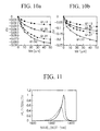
- FIG. 7 shows an example of the lattice matching conditions for InGaAsP having a band gap wavelength of 1.27 ⁇ m (hereinafter denoted as Q1.27) with a mask width Wm of 25 ⁇ m.
- the PL intensity is shown in FIG. 7a
- the PL line width is shown in FIG. 7b, both measured on an InGaAsP crystal grown by the selective MOVPE process for various combinations of the values of the As/P ratio and In/Ga ratio such that the band gap wavelength (PL peak wavelength) becomes 1.27 ⁇ 0.005 ⁇ m with a mask pattern having a width (Wm) of 25 ⁇ m.
- the variation in the proportion of As ( ⁇ y) is plotted along the abscissa in both FIG. 7a and FIG. 7b.
- the value of ⁇ y is the variation from that of the lattice matching conditions for non-selective MOVPE growth of Q1.27 having an InGaAsP composition of In x Ga 1-x As y P 1-y (0 ⁇ x ⁇ 1,0 ⁇ y ⁇ 1).
- FIG. 7 shows the PL intensity and the PL half-width value as functions of the variation in the proportion As/P of the group V composition
- the same data can be represented as functions of the variation in the proportion In/Ga of the group III composition, as shown in FIG. 8.
- the PL intensity is plotted in FIG. 8a, and the PL half-width value is plotted in FIG. 8b as a function of ⁇ x (deviation of the In proportion from the lattice matching condition for a non-selective MOVPE) which is plotted along the abscissa.
- a strained InGaAsP multi-quantum well (MQW) having a 1.3 ⁇ m band had made by using the selective MOVPE conditions for InGaAsP which had been derived; the PL characteristic evaluation results are described below.
- a mask width of Wm 25 ⁇ m was used for this selective growth.
- the quantum well structure was formed using strained InGaAsP with 1.0% of compressive strain introduced by shifting the proportion of the group III element from that of the lattice matching condition of Q1.27 as the well layer; and lattice-matched Q1.13 for the barrier layer.
- the thickness of the well layer and that of the barrier layer were set to 5 nm and 10 nm, respectively, and the number of repetitions of the MQW structure was set to 8 cycles.
- Light confinement (SCH) layers comprising lattice-matched Q1.13 having a thickness of 60 nm were provided above and below the MQW structure.
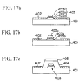
- FIG. 11 shows the PL spectra of the strained MQW structure which was grown by the selective MOVPE process.
- the solid line indicates the spectrum of Q1.27 and Q1.13 grown under the conditions of ⁇ x and ⁇ y shown in FIG. 10, and the dashed line indicates the spectrum for the case of growing under the conventional conditions wherein the variation in the proportion of the group V element is not taken into consideration. While the spectrum of the PL intensity represented by the solid line, which accounts for the variation in the proportion of the group V element, has a very small half-width of 25 meV, the spectrum of the conventional conditions represented by the dashed line has a large half-width of 44 meV with the PL peak intensity decreasing by 40% or more.
- the well layer does not include a desired amount of strain introduced therein when the variation in the proportion of the group V element is not taken into consideration, and the barrier layer and the SCH layer are not lattice-matched to the InP substrate, and therefore crystal defects are included.
- FIG. 12 shows a process of manufacturing a semiconductor laser (optical semiconductor device) of this embodiment.
- FIG. 13 is a schematic perspective view of the semiconductor laser (optical semiconductor device) of this embodiment.
- reference numeral 201 denotes a (100) InP substrate.
- the semiconductor laser of this embodiment has a strained InGaAsP MQW structure 203 formed in a stripe pattern in the [011] direction on the (100) InP substrate 201 which has an n-type electrode 211 on the under side thereof as shown in FIG. 13.
- Such a structure is formed by the selective MOVPE process as an InGaAsP-MQW structure layer 203b is sandwiched by an n-InP layer 203a and a p-InP layer 203c.
- p-InP layers 205 are formed at a position higher than the top surface of the p-InP layer 203c on both sides of the MQW structure 203, with an n-InP layer 206 being provided on the p-InP layer 205.
- the entire surfaces of the p-InP layer 203c and the n-InP layer 206 are covered by a p-InP cladding layer 207.
- the bottom of the p-InP cladding layer 207 is embedded in a trough formed by the p-InP layer 205 and the n-InP layer 206 in which the strained MQW structure 203 is located, and is connected to the n-InP layer 206.
- the p-InP cladding layer 207 is covered by a p+-InGaAs layer 208 over the entire surface thereof, while a p-type electrode 210 formed in a pattern corresponding to the strained MQW structure 203 is provided on the p+-InGaAs layer 208.
- An SiO 2 layer 209 covers the surface except for the p-type electrode 210 on the p + -InGaAs layer 208.
- a pair of SiO 2 stripe masks 202 are patterned at a 1.5 ⁇ m interval in the [011] direction on the (100) n-InP substrate 201 as shown in FIG. 12.
- the mask width (Wm) of the SiO 2 stripe masks 202 is set to 25 ⁇ m (FIG. 12a).
- the strained InGaAsP MQW structure 203 is formed on the patterned substrate 201 by the selective MOVPE process.
- the growth temperature is set to 625°C, and the growth pressure is set to 1000 hPa.
- the structure formed by the selective MOVPE process comprises the n-InP layer 203a, the strained InGaAsP-MQW structure layer 203b, and the p-InP layer 203c as shown in FIG. 12(b).
- the strained MQW structure layer 203b has an SCH layer added thereto such that it is formed by stacking a set of an InGaAsP layer (5 nm thick), with 1.0% of compressive strain introduced therein by shifting the proportion of the group III element from that of the lattice matching condition of Q1.27 as the well layer, and a lattice-matched Q1.13 layer (10 nm thick) as the barrier layer in eight cycles, with a Q1.13 layer (60 nm thick) being lattice-matched to the top and bottom of the repeated structure described above.
- a SiO 2 mask 204 is formed only on the top surface of the selectively grown mesa 203 as shown in FIG. 12(c). This process is carried out similar to that described in detail by Y. Sakata et al. in the IEEE Journal of Quantum Electronics, Vol. 35, pp. 368 - 376, 1999.
- the semiconductor laser structure as shown in FIG. 13 is formed through a process of forming electrodes.
- the characteristics of the laser were evaluated by applying a highly specular coating having a high reflectance of 95% on the rear end of a resonator made to a length of 300 ⁇ m.
- the laser showed an oscillation threshold current of 3.5 mA, a slope efficiency of 0.62 W/A, and an oscillation wavelength of 1.315 nm at room temperature of 25°C. At a temperature of 85°C, a low oscillation threshold current of 7.9 mA and a high slope efficiency of 0.48 W/A were confirmed. Then an experiment of transmission at 622 Mb/s was conducted with this device; good eye aperture was verified, and the capability of transmission at 622 Mb/s was confirmed over a temperature range from -40 to +85°C.
- the semiconductor laser of this embodiment has the effect of improving the characteristics of the semiconductor optical device formed by the selective MOVPE growth process.
- FIGS. 14(a) and (b) show a process of manufacturing a semiconductor laser (optical semiconductor device) of this embodiment.
- This embodiment is adapted to a 1.3 ⁇ m band semiconductor laser with a spot size converter integrated therein.
- the device of this embodiment has a spot size converter (SCC), which enlarges the beam spot at the laser beam emitting end, integrated therein, with the beam spread angle being as small as 1/2 to 1/3 of those of conventional lasers, making it possible to efficiency couple with an optical fiber without using a lens.
- SCC spot size converter
- the semiconductor laser of this embodiment comprises a strained InGaAsP MQW structure 303 formed in the [011] direction on a (100) InP substrate 301 as shown in FIG. 14(b) similar to the first embodiment shown in FIG. 13.
- a constitution of this embodiment other than the above has a structure corresponding to the p-InP layer 205, the n-InP layer 206, the p-InP cladding layer 207, the p + -InGaAs layer 208, the p-type electrode 210, and the SiO 2 layer 209 shown in the first embodiment, but is not shown in the drawing.
- the semiconductor laser of this embodiment is made by patterning a pair of SiO 2 masks 302 as shown in FIG. 14(a) at a 1.5 ⁇ m interval in the [011] direction on the (100) InP substrate 301.
- the n-InP/strained MQW/p-InP structure 303 is formed on the substrate 301 which was patterned as described above by the selective MOVPE process on the substrate 303 which was patterned as described above, similar to the first embodiment.
- the growing conditions are also the same as those of the first embodiment.
- the laser region 302a reproduced the PL characteristic shown by the solid line in FIG. 11.
- an SSC integrated semiconductor laser was made by the same process as that of the first embodiment shown in FIG. 12 and FIG. 13.
- the characteristics of the laser were evaluated by applying a high-reflection coating having a reflectance of 95% to the rear end face on the laser side, with the laser made to a total length of 500 ⁇ m, or 300 ⁇ m of the laser region plus 200 ⁇ m of the SSC region.
- the laser showed an oscillation wavelength of 1315 nm, an oscillation threshold current of 5.5 mA, and a slope efficiency of 0.55 W/A at room temperature of 25°C.
- the oscillation wavelength was 1.336 nm
- the oscillation threshold current was 12.5 mA
- the slope efficiency was 0.45 W/A.
- Measurement of the far field pattern (FFP) showed a beam spread angle of 27° ⁇ 30° at the rear end face and a spread angle of 10.5° ⁇ 11.0° at the front end face. Then the characteristic of coupling with a flat-end single-mode fiber (1.3 ⁇ m, zero dispersion) with an anti-reflection coating applied to the end face thereof was evaluated. A maximum coupling efficiency of -2.2 dB was obtained when the laser was brought to a distance of 10 ⁇ m from the fiber.
- the semiconductor laser of this embodiment has the effect of improving the characteristics of the semiconductor optical device formed by the selective MOVPE growth process.
- FIG. 15, FIG. 16, and FIG. 17 show a process of manufacturing a semiconductor laser (optical semiconductor device) of this embodiment.
- FIG. 18 is a schematic perspective view of the semiconductor laser (optical semiconductor device) of this embodiment.
- This embodiment is adapted to an electro-absorption (EA) type modulator-integrated distributed feedback (DFB) semiconductor laser.
- EA electro-absorption
- DFB distributed feedback
- the semiconductor laser of this embodiment comprises a strained InGaAsP MQW structure 403 formed in the [011] direction on the (100) InP substrate 301 as shown in FIG. 16 similar to the first embodiment shown in FIG. 13 and the second embodiment shown in FIG. 14.
- the strained MQW structure 403 is covered, on the central portion thereof having a width of 1.5 ⁇ m, by a p-InP cladding layer 404 which is wide enough to extend beyond the central portion.
- the p-InP cladding layer 404 is formed on the strained MQW structure 403 also outside the mask pattern.
- a p + -InGaAs cap layer 405 is formed on the p-InP cladding layer 404.
- a portion, measuring 30 ⁇ m, of the p + -InGaAs cap layer 405 is removed between the DFB laser region 402a and the EA modulator region 402b, and a p-type electrode 407 is formed via an SiO 2 film 406 as an inter-layer film as shown in FIG. 18.
- An n-type electrode 408 is formed over the entire surface of the back of the n-InP substrate 401.
- the diffraction grating 400 is partially formed on the (100) InP substrate 401 by electron beam exposure and wet etching as shown in FIG. 15.
- the pair of SiO 2 masks 402 are formed at a 1.5 ⁇ m interval in the [011] direction.
- the strained InGaAsP well layer has a proportion of a group III element which has been changed from that of the lattice matching condition of Q1.50 so that a compressive strain of +0.50% would be introduced.
- the selective growing conditions for Q1.20 and the strained Q1.50 will be described in detail below.
- the p + -InGaAs cap layer 405 measuring 30 ⁇ m is removed between the DFB laser region 402a and the EA modulator region 402b thereby establishing electrical isolation, and the p-type electrode 407 is formed with the SiO 2 film 406 used as an inter-layer film as shown in FIG. 18.
- the n-type electrode 408 is formed by polishing the back of the n-InP substrate 401 until the thickness becomes 120 ⁇ m.
- this semiconductor laser was evaluated by applying a high-reflection coating having a reflectance of 95% to the end face of the DFB laser side and an anti-reflection coating having a reflectance below 0.1% to the end face of the modulator side, with the laser made to a total length of 600 ⁇ m, or 400 ⁇ m of the DFB laser region plus 200 ⁇ m of the EA modulator region.
- the laser showed an oscillation threshold current of 4.5 mA and a high slope efficiency of 0.30 W/A, and an optical output power of 16 mW was obtained when a current of 60 mA was input into the DFB laser and the bias voltage for the EA modulator was set to 0 V.
- An extinction ratio (ON/OFF ratio) of as high as -25 dB was obtained when a voltage of -2 V was applied to the EA modulator. This is because a large variation in the absorption coefficient was achieved when the electric field was applied due to good crystalline property.
- This device was used in an experiment of transmission over 1,000 km at 2.5 Gb/s through a zero-dispersion single-mode fiber of 1.3 ⁇ m, with a satisfactory power penalty result below 1.5 dB as evaluated with a coding error ratio of 10 -11 .
- the semiconductor laser of this embodiment has the effect of improving the characteristics of the semiconductor optical device formed by the selective MOVPE growth process.
- FIG. 19 is a schematic perspective view of the optical module (optical communication module) of this embodiment.
- This embodiment is adapted to an optical communication module provided with an electro-absorption (EA) type modulator-integrated distributed feedback (DFB) semiconductor laser of the third embodiment.
- EA electro-absorption
- DFB distributed feedback
- the optical communication module of this embodiment comprises an optical semiconductor device 502 having a constitution which corresponds to the electro-absorption (EA) type modulator integrated distributed feedback (DFB) semiconductor laser of the third embodiment, an aspherical lens 503, an optical isolator 504, and an electrical interface 501, while an optical fiber 505 is connected thereto as shown in FIG. 19.
- EA electro-absorption
- DFB distributed feedback
- the optical communication module is configured so that the optical output from the optical semiconductor device 502 is sent through the aspherical lens 503 and the optical isolator 504 to the optical fiber 505, while the electrical interface 501 is incorporated for driving the optical semiconductor device 502.
- the optical communication module of this embodiment makes it possible to generate high speed optical communication signals very efficiently. This is because the optical semiconductor device of the present invention has a low threshold and high efficiency during operation.
- FIG. 20 is a schematic perspective view of an optical communication system of this embodiment.
- This embodiment is adapted to a wavelength division multiplexing (WDM) optical communication system provided with the optical communication module 500 of the fourth embodiment.
- WDM wavelength division multiplexing
- the optical communication system of this embodiment comprises an optical transmitter 600 and an optical receiver 601 which are connected together via the optical fiber 505 as shown in FIG. 20.
- the optical transmitter 600 comprises 64 optical transmission modules 500 having different emission wavelengths, an optical multiplexer 605 which multiplexes light signals from the optical transmission modules 500, and a drive unit 602 which drives the optical transmission modules 500.
- the optical receiver 601 comprises 64 optical reception modules 603 which correspond to different wavelengths of the optical transmission modules 500, an optical demultiplexer 606 connected to the optical fiber 505, and an optical reception module drive unit 604 which drives the optical reception modules 603.
- signal light which is output from the optical transmitter 600 is sent through the optical fiber 505 to the optical receiver 601.
- Optical signals of 64 different wavelengths which have been input into the optical receiver 601 are sent through the optical demultiplexer 606 and input into the 64 optical reception modules 603 that are controlled by the optical reception module drive unit 604, thereby detecting the signals.
- the optical communication module of the present invention makes it possible to easily achieve WDM transmission. This is because the optical semiconductor device employed in the optical transmitter has a low threshold and high optical output power.
- the present invention is not limited to these embodiments and can be applied to any optical semiconductor devices which use a III-V compound semiconductor formed by the selective MOVPE process as the major component.
- the present invention can be applied to a semiconductor optical modulator, a semiconductor optical detector, a semiconductor optical switch, and a semiconductor optical waveguide, or semiconductor optical devices which integrate these components.
- the embodiments described above deal only with such cases as a narrow-width selective MOVPE process which allows it to directly form the semiconductor optical waveguide structure without etching the semiconductor layer.
- the present invention can also be applied to a large-width selective MOVPE process wherein the selective growth region is made several micrometers or wider.
- optical semiconductor device and the method for manufacturing the same according to the present invention, and the optical module or the optical communication apparatus employing the semiconductor optical device are constituted as described above, and are capable of obtaining a high quality semiconductor crystal and improving the device characteristics by taking into consideration the effects of varying the proportion of the group V element (As/P) which has been ignored in the prior art when setting the conditions for growing the crystal, for the case when the InGaAsP layer formed by the selective MOVPE process is the major component.
- group V element As/P
Landscapes
- Physics & Mathematics (AREA)
- Condensed Matter Physics & Semiconductors (AREA)
- General Physics & Mathematics (AREA)
- Electromagnetism (AREA)
- Optics & Photonics (AREA)
- Semiconductor Lasers (AREA)
- Optical Couplings Of Light Guides (AREA)
- Physical Deposition Of Substances That Are Components Of Semiconductor Devices (AREA)
- Optical Modulation, Optical Deflection, Nonlinear Optics, Optical Demodulation, Optical Logic Elements (AREA)
- Light Receiving Elements (AREA)
Applications Claiming Priority (2)
| Application Number | Priority Date | Filing Date | Title |
|---|---|---|---|
| JP2000207462A JP2002026461A (ja) | 2000-07-07 | 2000-07-07 | 光半導体装置とその製造方法および光半導体装置を備えた光装置モジュール、光通信装置 |
| JP2000207462 | 2000-07-07 |
Publications (2)
| Publication Number | Publication Date |
|---|---|
| EP1170841A2 true EP1170841A2 (de) | 2002-01-09 |
| EP1170841A3 EP1170841A3 (de) | 2003-05-21 |
Family
ID=18704219
Family Applications (1)
| Application Number | Title | Priority Date | Filing Date |
|---|---|---|---|
| EP01116355A Withdrawn EP1170841A3 (de) | 2000-07-07 | 2001-07-05 | Optische Halbleitervorrichtung und zugehöriges Herstellungsverfahren |
Country Status (4)
| Country | Link |
|---|---|
| US (1) | US20020003914A1 (de) |
| EP (1) | EP1170841A3 (de) |
| JP (1) | JP2002026461A (de) |
| CA (1) | CA2352641A1 (de) |
Families Citing this family (6)
| Publication number | Priority date | Publication date | Assignee | Title |
|---|---|---|---|---|
| KR100446615B1 (ko) * | 2001-10-09 | 2004-09-04 | 삼성전자주식회사 | 반도체 레이저 다이오드 및 그 제조방법 |
| JP2004095859A (ja) * | 2002-08-30 | 2004-03-25 | Sharp Corp | 半導体レーザ及びその製造方法 |
| KR100875929B1 (ko) * | 2006-12-05 | 2008-12-26 | 한국전자통신연구원 | 반도체막의 선택적 영역 성장용 마스크 패턴 및 그를이용한 반도체막의 선택적 영역 성장 방법 |
| JP6423159B2 (ja) * | 2014-02-27 | 2018-11-14 | 富士通株式会社 | Ge系半導体装置、その製造方法及び光インターコネクトシステム |
| JP6903896B2 (ja) * | 2016-01-13 | 2021-07-14 | ソニーグループ株式会社 | 受光素子の製造方法 |
| CN111785746A (zh) * | 2020-07-13 | 2020-10-16 | 中国科学技术大学 | 一种多通道高速探测器芯片 |
Family Cites Families (4)
| Publication number | Priority date | Publication date | Assignee | Title |
|---|---|---|---|---|
| JP2842292B2 (ja) * | 1994-09-16 | 1998-12-24 | 日本電気株式会社 | 半導体光集積装置および製造方法 |
| JPH08307012A (ja) * | 1995-05-01 | 1996-11-22 | Mitsubishi Electric Corp | 選択成長用マスク,半導体光装置の製造方法,および半導体光装置 |
| JPH1075009A (ja) * | 1996-08-30 | 1998-03-17 | Nec Corp | 光半導体装置とその製造方法 |
| JP3186704B2 (ja) * | 1998-08-05 | 2001-07-11 | 日本電気株式会社 | 半導体非線形導波路及び光スイッチ |
-
2000
- 2000-07-07 JP JP2000207462A patent/JP2002026461A/ja active Pending
-
2001
- 2001-07-05 EP EP01116355A patent/EP1170841A3/de not_active Withdrawn
- 2001-07-05 CA CA002352641A patent/CA2352641A1/en not_active Abandoned
- 2001-07-06 US US09/899,274 patent/US20020003914A1/en not_active Abandoned
Also Published As
| Publication number | Publication date |
|---|---|
| JP2002026461A (ja) | 2002-01-25 |
| CA2352641A1 (en) | 2002-01-07 |
| EP1170841A3 (de) | 2003-05-21 |
| US20020003914A1 (en) | 2002-01-10 |
Similar Documents
| Publication | Publication Date | Title |
|---|---|---|
| EP0836255B1 (de) | Laserdioden-Array und Herstellungsverfahren | |
| EP0682390B1 (de) | Vorrichtung und Verfahren zur Steuerung einer polarisationsselektiver Lichtquelle, und optisches Kommunikationssystem unter Verwendung desselben | |
| US6134368A (en) | Optical semiconductor device with a current blocking structure and method for making the same | |
| JP3285426B2 (ja) | 半導体光集積素子及びその製造方法 | |
| EP0959540B1 (de) | Halbleiterlaser mit erhöhter Ausgangsleistung | |
| US7809038B2 (en) | Electro-absorption optical modulator integrated with a laser to produce high speed, uncooled, long distance, low power, 1550 nm optical communication device with optimized parameters | |
| EP0921615B1 (de) | Halbleiterlaser mit verteilter Rückkoppelung und unterschiedlichen Lichtintensitätsverteilungen der verschiedenen Polarisationsmoden, sowie zugehöriges Ansteuerverfahren | |
| JPH0738204A (ja) | 半導体光デバイス及びその製造方法 | |
| EP0846967B1 (de) | Optische Halbleitervorrichtung und Herstellungsverfahren | |
| US8179592B2 (en) | Semiconductor optical amplifier, method for manufacturing the same, and semiconductor optical integrated device | |
| US5822352A (en) | Optical semiconductor apparatus, fabrication method thereof, modulation method therefor, light source apparatus and optical communication system using the same | |
| EP0661783B1 (de) | Verfahren zur Herstellung eines integrierten, optischen Halbleiterschaltkreises | |
| EP1170841A2 (de) | Optische Halbleitervorrichtung und zugehöriges Herstellungsverfahren | |
| US8749879B2 (en) | Semiconductor optical amplifier and optical amplification apparatus | |
| US20050185689A1 (en) | Optoelectronic device having a Discrete Bragg Reflector and an electro-absorption modulator | |
| US5756373A (en) | Method for fabricating optical semiconductor device | |
| EP0316194B1 (de) | Filter mit abstimmbarer Wellenlänge | |
| EP0615322B1 (de) | Multiquantumwell-Halbleiterlaser und optisches Kommunikationssystem mit einem derartigen Laser | |
| Chuang et al. | Enhanced wavelength tuning in grating-assisted codirectional coupler filter | |
| JP2001326414A (ja) | 光半導体装置とその製造方法 | |
| JP2010114158A (ja) | 電界吸収型光変調器集積レーザ素子の製造方法 | |
| KR100745918B1 (ko) | 반도체 광 소자, 반도체 광 소자의 제조 방법 및 광 모듈 | |
| US20260011975A1 (en) | Semiconductor optical device and manufacturing method thereof | |
| US7286588B2 (en) | Semiconductor laser with grating structure for stabilizing the wavelength of optical radiation | |
| JP2001142036A (ja) | 半導体光変調器およびその製造方法 |
Legal Events
| Date | Code | Title | Description |
|---|---|---|---|
| PUAI | Public reference made under article 153(3) epc to a published international application that has entered the european phase |
Free format text: ORIGINAL CODE: 0009012 |
|
| AK | Designated contracting states |
Kind code of ref document: A2 Designated state(s): AT BE CH CY DE DK ES FI FR GB GR IE IT LI LU MC NL PT SE TR |
|
| AX | Request for extension of the european patent |
Free format text: AL;LT;LV;MK;RO;SI |
|
| PUAL | Search report despatched |
Free format text: ORIGINAL CODE: 0009013 |
|
| RAP1 | Party data changed (applicant data changed or rights of an application transferred) |
Owner name: NEC ELECTRONICS CORPORATION |
|
| AK | Designated contracting states |
Designated state(s): AT BE CH CY DE DK ES FI FR GB GR IE IT LI LU MC NL PT SE TR |
|
| AX | Request for extension of the european patent |
Extension state: AL LT LV MK RO SI |
|
| 17P | Request for examination filed |
Effective date: 20030417 |
|
| 17Q | First examination report despatched |
Effective date: 20030715 |
|
| STAA | Information on the status of an ep patent application or granted ep patent |
Free format text: STATUS: THE APPLICATION HAS BEEN WITHDRAWN |
|
| 18W | Application withdrawn |
Effective date: 20031009 |