EP1170859B1 - Verzerrungsausgleichverfahren und Gerät - Google Patents
Verzerrungsausgleichverfahren und Gerät Download PDFInfo
- Publication number
- EP1170859B1 EP1170859B1 EP01305186A EP01305186A EP1170859B1 EP 1170859 B1 EP1170859 B1 EP 1170859B1 EP 01305186 A EP01305186 A EP 01305186A EP 01305186 A EP01305186 A EP 01305186A EP 1170859 B1 EP1170859 B1 EP 1170859B1
- Authority
- EP
- European Patent Office
- Prior art keywords
- distortion
- adaptive
- correction data
- signal
- phase
- Prior art date
- Legal status (The legal status is an assumption and is not a legal conclusion. Google has not performed a legal analysis and makes no representation as to the accuracy of the status listed.)
- Expired - Lifetime
Links
Images








Classifications
-
- H—ELECTRICITY
- H03—ELECTRONIC CIRCUITRY
- H03F—AMPLIFIERS
- H03F1/00—Details of amplifiers with only discharge tubes, only semiconductor devices or only unspecified devices as amplifying elements
- H03F1/32—Modifications of amplifiers to reduce non-linear distortion
- H03F1/3241—Modifications of amplifiers to reduce non-linear distortion using predistortion circuits
- H03F1/3247—Modifications of amplifiers to reduce non-linear distortion using predistortion circuits using feedback acting on predistortion circuits
-
- H—ELECTRICITY
- H03—ELECTRONIC CIRCUITRY
- H03F—AMPLIFIERS
- H03F1/00—Details of amplifiers with only discharge tubes, only semiconductor devices or only unspecified devices as amplifying elements
- H03F1/32—Modifications of amplifiers to reduce non-linear distortion
- H03F1/3241—Modifications of amplifiers to reduce non-linear distortion using predistortion circuits
- H03F1/3282—Acting on the phase and the amplitude of the input signal
-
- H—ELECTRICITY
- H03—ELECTRONIC CIRCUITRY
- H03F—AMPLIFIERS
- H03F2200/00—Indexing scheme relating to amplifiers
- H03F2200/102—A non-specified detector of a signal envelope being used in an amplifying circuit
Definitions
- This invention relates to a distortion compensation apparatus. More particularly, it relates to a method and apparatus applicable to a high frequency power amplifier for transmission usable in particular in a portable telephone set.
- FIG. 1 shows a block diagram of a technique introduced e.g., in 1992. European Microwave Conference Vol.22, pp.1125 to pp.1130, "Power Amplifier Adaptive Linearization Using Predistortion with Polynominal ".
- in-phase and quadrature signals I, Q of the input baseband to be input at an input terminal 111 may be calculated by a linearization comparator circuit 112 using a function H(I, Q) which linearizes A(Vin).
- the resulting I, Q signals are fed to a digital to analog converter (DAC) 113 and thereby analogized, while being converted into high frequency band signals which are input to a power amplifier 114.
- DAC digital to analog converter
- An output Vout of the power amplifier 114 is detected and output from an output terminal 115, at the same time as it is converted in a demodulator circuit 116 into baseband signals If and Qf.
- the linearization comparator circuit 112 compares the input signals I, Q to detection signals If, Qf to adjust a constant in a linearization function H so that a difference therebetween will be equal to zero. This operation is repeated until the difference is correctly equal to zero to set the constant in the function H (I, Q) ultimately to a proper value.
- Fig.2 shows a block diagram disclosed in this publication. In Fig.2 , those parts or components corresponding to those shown in Fig.1 are denoted by the same reference numerals.
- a conversion table 124 such as a memory, is accessed for the input signals I and Q to effect data conversion to derive data I', Q' capable of linearizing the power amplifier 114. These data I', Q' are input to the power amplifier 114.
- An output Vout of the power amplifier 114 is detected and converted in a demodulator 116 to produce signals If, Qf.
- an address generator 123 for comparing the input signals I, Q to detection signals If, Qf from the demodulator 116 to adjust the address for accessing the conversion table 124 so that a difference en will be zero. The address generator 123 is repeatedly adjusted until the difference en is correctly zero to optimize the address value which accesses the conversion table 124.
- the constant included in the linearization function or the address for accessing the linearization table is optimized.
- repetitive operations are carried out using a feedback loop to reduce the difference.
- the feedback loop suffers a serious problem that the loop contains characteristics of the power amplifier 114 such that there is no guarantee that the convergence to an optimum value in stability will be realized at all times.
- the above-described structures are in need of a demodulator in order to effect conversion of the power amplifier output into the baseband output. Since this demodulator is in general a quadrature demodulator, the circuit scale is voluminous.
- US-A-5 093 637 discloses a modulation system using an amplitude and a phase of a carrier wave as information to modify an input signal series to compensate the nonlinear characteristics of an amplifier located at a later stage, and provide a carrier wave modulated by the modified signal series to the amplifier.
- a first arithmetic circuit obtains an amplitude and a phase of an input signal by calculation.
- a ROM is set with correction data corresponding to the calculated amplitude so as to compensate the nonlinearity of the amplifier.
- a modification value generating circuit and a RAM output an amount of compensation so as to further modify the correction data according to part of an output signal from the amplifier to compensate amplifier characteristic changes due to temperature variations and the like.
- a second arithmetic circuit provides a signal series produced from the modified amplitude and phase to a quadrature modulator.
- CA-A-2 291 863 discloses a linear power amplifier comprising a power amplifier, a feedback circuit and a control element; wherein the architecture proposed uses an envelope detector to generate a base band signal representing the amplitude envelope of the system input RF signal. This is digitized and used to generated phase and gain correction signals. The correction signals modulate the input signal to create a pre-distorted signal: which is applied to the power amplifier for amplification.
- the method disclosed incorporates an adaptation system whereby the pre-distorter can learn the contents of a lookup table as it operates.
- the distortion compensation apparatus includes amplitude distortion correcting means for outputting correction data for correcting the amplitude distortion of the device based on the envelope signal of the input signal supplied to the device, and for controlling the gain changing processing of the device responsive to the correction data to correct the amplitude distortion of the device.
- the adaptive amplitude distortion compensation means sums the adaptive correction data to the correction data used in the amplitude distortion correcting means to effect adaptive compensation of the amplitude distortion of the device.
- the adaptive amplitude distortion compensation means includes first envelope detection means for detecting an envelope signal of an input signal supplied to the device, second envelope detection means for detecting the envelope component of an output signal of the device, subtraction means for finding an amplitude difference between the envelope component of the input signal as detected by the second envelope detection means, cumulating means for integrating and cumulating the amplitude difference as obtained by the subtraction means and adaptive correction data outputting means for outputting adaptive correction data against temperature fluctuations in the device based on the cumulated results in the cumulating means.
- the distortion compensation apparatus includes adaptive phase distortion compensation means for outputting adaptive phase distortion correction data against temperature fluctuations of the device based on a phase different between an input signal supplied to the device and an output signal from the device and for adaptively compensating the phase distortion of the device using the adaptive correction data.
- the distortion compensation apparatus further includes phase distortion correction means for outputting correction data for correcting the phase distortion of the device based on an envelope signal of an input signal supplied to the device and for controlling the phase shifting processing of the device responsive to the correction data to correct the phase distortion of the device.
- phase distortion correction means for outputting correction data for correcting the phase distortion of the device based on an envelope signal of an input signal supplied to the device and for controlling the phase shifting processing of the device responsive to the correction data to correct the phase distortion of the device.
- the adaptive phase distortion compensation means sums the adaptive correction data to the correction data used in the phase distortion correcting means to adaptively compensate the phase distortion of the device.
- the adaptive phase distortion compensation means includes phase different detection means for detecting the phase different between an input signal supplied to the device and an output signal from the device and adaptive phase distortion correcting data outputting means for outputting adaptive phase distortion correction data against temperature fluctuations of the device based on the phase difference as detected by the phase different detection means.
- the distortion compensation method further includes an amplitude distortion correcting step for outputting correction data for correcting the amplitude distortion of the device based on the envelope signal of the input signal supplied to the device, and for controlling the gain changing processing of the device responsive to the correction data to correct the amplitude distortion of the device.
- an amplitude distortion correcting step for outputting correction data for correcting the amplitude distortion of the device based on the envelope signal of the input signal supplied to the device, and for controlling the gain changing processing of the device responsive to the correction data to correct the amplitude distortion of the device.
- the adaptive amplitude distortion compensation step sums the adaptive correction data to the correction data used in the amplitude distortion correcting step to effect adaptive compensation of the amplitude distortion of the device.
- the distortion compensation method further includes an adaptive phase distortion compensation step for outputting adaptive phase distortion correction data against temperature fluctuations of the device based on a phase different between an input signal supplied to the device and an output signal from the device and for adaptively compensating the phase distortion of the device using the adaptive correction data.
- an adaptive phase distortion compensation step for outputting adaptive phase distortion correction data against temperature fluctuations of the device based on a phase different between an input signal supplied to the device and an output signal from the device and for adaptively compensating the phase distortion of the device using the adaptive correction data.
- the distortion compensation method further includes a phase distortion correction step for outputting correction data for correcting the phase distortion of the device based on an envelope signal of an input signal supplied to the device and for controlling the phase shifting processing of the device responsive to the correction data to correct the phase distortion of the device.
- a phase distortion correction step for outputting correction data for correcting the phase distortion of the device based on an envelope signal of an input signal supplied to the device and for controlling the phase shifting processing of the device responsive to the correction data to correct the phase distortion of the device.
- the adaptive phase distortion compensation step sums the adaptive correction data to the correction data used in the phase distortion correcting step to adaptively compensate the phase distortion of the device.
- distortion components in the power amplifier can be compensated extremely readily using a method comprised of envelope detection without resorting to quadrature demodulation. Moreover, since the distortion component is detected by integration of an output input difference to effect distortion compensation, even the slightest distortion compensation can be detected.
- This distortion compensation apparatus is designed to compensate the distortion in a high frequency power amplifier in a digital radio communication apparatus, abbreviated herein to power amplifier.
- This distortion compensation apparatus is mainly constituted by four channels, namely an amplitude distortion correcting channel, as a channel for correcting the amplitude distortion of the power amplifier, a phase distortion correcting channel, as a channel for correcting the phase distortion of the power amplifier, a channel for adaptive compensation of the amplitude distortion accompanying variations in the power amplifier temperature and a channel traversed by high frequency signals reaching the power amplifier.
- the amplitude distortion correcting channel is the amplitude distortion correcting means for outputting correction data for correcting the amplitude distortion of the power amplifier based on envelope signals of high frequency input signals supplied to the power amplifier to control the gain changing processing of the power amplifier responsive to the correction data to correct the amplitude distortion of the power amplifier.
- the phase shifting correcting channel is the phase distortion correcting means for outputting correction data for correcting the phase distortion of the power amplifier based on envelope signals of high frequency input signals supplied to the power amplifier to control the phase shifting processing of the power amplifier responsive to the correction data to correct the phase distortion of the power amplifier.
- the channel for adaptive compensation of the amplitude distortion is the adaptive amplitude distortion compensation means and finds the amplitude difference between the envelope signal of an input signal supplied to te power amplifier and the envelope signal of an output signal of the power amplifier to output adaptive amplitude distortion correction data against temperature variations of the power amplifier based on results corresponding to integration and cumulation of the amplitude differences to effect adaptive compensation of the amplitude distortion of the power amplifier.
- the amplitude distortion correcting channel includes an envelope detection unit (DET 1 ) 1, fed with a portion of a high frequency signal S1, undergoing variations in an envelope S2, and adapted for detecting the envelope S2, and an A/D converter 3 for digitizing the envelope S2 after passage thereof through a first selector (SEL 1 ) 2, and for outputting a digital signal S21.
- EDT 1 envelope detection unit
- SEL 1 first selector
- the amplitude distortion correcting channel also includes a first memory (M 1 ) 6 which is fed as an address with a signal S3 corresponding to this digital signal S21 passed through a second selector (SEL 2 ) 4 and held by a second latch (LCH 2 ) 5 and which outputs amplitude correction data S7, corresponding to this address, pre-stored for amplitude correction, and a second adder (ADD 2 ) 7 for summing an output S7 of the first memory 6 to a digital signal S44 as later explained.
- M 1 first memory
- SEL 2 second selector
- LCH 2 second latch
- ADD 2 second adder
- the amplitude distortion correcting channel also includes a first D/A converter (D/A 1 ) 8 for analogizing summed results S9 of the second adder 7, and a first low-pass filter (LPF 1 ) 9 for removing the digital noise contained in the analog signal from the first D/A converter 8.
- D/A 1 first D/A converter
- LPF 1 first low-pass filter
- the phase distortion correction channel includes a second memory (M 2 ) 10 for outputting phase correction data S4 corresponding to the digital signal S3, which is data pre-stored for phase correction, a second D/A converter (D/A 2 ) 11 for analogizing an output S9 of the second memory 10 and a second low-pass filter (LPF 2 ) 12 for removing the digital noise contained in the analog signal from the second D/A converter 11.
- the adaptive compensation channel for the amplitude distortion includes a random access memory (RAM 1 ) 17 for reading out data stored in association with an address which is the aforementioned digital signal S3, and for outputting the read-out signal, or writing a signal S41 as later explained, and a second envelope detection unit (DET 2 ) 13 for detecting an envelope S31 of an output S30 of a power amplifier (PA) 23, the distortion of which is to be compensated.
- RAM 1 random access memory
- PA power amplifier
- the adaptive compensation channel for the amplitude distortion includes a subtractor (SUB) 15 for digitally subtracting, from the digital signal S3, a signal S24 obtained on passing the envelope S31 through the first selector 2, digitizing the envelope by the A/D converter 3, passing the digitized envelope through a second selector 4 and on latching the result in a third latch (LCH 3 ) 14, and a first adder (ADD 1 ) 16 for digitally summing the digital signal S40 to a digital signal S43 as later explained to output the result as a signal S41, and the first latch circuit (LCH 1 ) to latch the output signal S42 of the random access memory 17 as a S43.
- the adaptive compensation channel for the amplitude distortion includes a third memory (M 3 ) fed with the latched signal S43 as address and adapted for outputting adaptive correction data S44, corresponding to this address, pre-stored for adaptive correction.
- the first adder 16, random access memory 17 and the first latch circuit 18 make up cumulation means, while the third memory 19 is adaptive correction data outputting means.
- the A/D converter used for this channel, is used for digitizing the envelopes of the input signal S1 and the output signals S30 of the power amplifier 23, and uses a selector and a latch for selecting and holding these signals.
- the channel for passage of the high frequency signals includes a delay device (DL) 20, fed with the high frequency signal S1 and adapted for delaying the time of passage to give a signal S50, and a phase shifter (PH) 21, fed with an output 50 of the delay device 20 and having an output S6 of the second low-pass filter 13 coupled to its control terminal.
- the phase shifter 21 is able to change the passage phase of the input signal by the signal applied to the control terminal.
- the channel for passage of the high frequency signals also includes a gain changing unit (AM) 22, fed with an output 51 of the phase shifter 21 and having an output S11 of the first low-pass filter 9 coupled to its control terminal.
- the phase shifter 21 is able to change the passage gain by the signal applied to the control terminal.
- An output S52 of the gain changing unit 22 is input to the power amplifier 23 the distortion of which is to be corrected.
- This distortion compensation apparatus includes, in addition to the aforementioned respective channels, a clock generator (CLK) 24 for generating clock signals MRW for switching the read/write timing for the random access memory 17 and a clock generator CLK 24 for generating clock signals LC for permitting the latch circuits (LCH 1 to 3) to perform latching operations.
- CLK clock generator
- high frequency input signals S1 of quadrature phase modulated signals such as band-limited ⁇ /4 shift QPSK (quadrature phase shift keying) signals or 0° QPSK signals, as used in a portable telephone set, are fed to an input terminal Tin of the distortion compensation apparatus.
- This high frequency input signal S1 contains an envelope component modulating the high frequency carrier with a baseband signal component and which is gradually fluctuated as time elapses.
- the high frequency input signal S1, fed to the input terminal Tin is divided into two portions which are separately input to an amplitude distortion correcting channel and to a fourth channel.
- the high frequency input signal S1, input to the amplitude distortion correcting channel has its envelope signal S2 detected by an envelope detection circuit 1.
- the envelope signal S2, detected by the envelope detection circuit 1 is selected by a first selector 2 to prove a select output signal selector output signal S20 which is converted by the A/D converter 3 into the digital signal S21.
- This digital signal S21 is further selected by a second selector 4 to prove a selector output signal S23 which then is held by a second latch 5 so as to be output as signal S3.
- This signal S3 is input as an address to the first memory 6, which has stored therein correction data for amplitude correction from the outset and which outputs to the adder 7 the amplitude correction data S7 associated with the aforementioned signal S3 as an address. Meanwhile, the signal S3 is also furnished to the second memory 10 of the phase distortion correction channel, to a subtractor 15 of the adaptive amplitude distortion compensating channel and to a random access memory 17, in a manner which will be explained subsequently.
- the adder 7 sums the amplitude correction data S7 to adaptive compensation data S44 as later explained to send the resulting sum output S9 to the first D/A converter 8.
- the first D/A converter 8 converts the sum output S9, that is the adaptive compensation data 544, summed to the amplitude correction data S7, into an analog signal S10, which then is sent to the first low-pass filter 9.
- the first low-pass filter 9 sends a filter output signal S11, corresponding to the analog signal S10 freed of the digital noise, to a control terminal of the gain changing unit 22 making up the high frequency signal passage channel.
- the gain changing unit 22 controls the passage gain (amplitude) with the signal S11 sent to the control terminal as a control signal.
- the amplitude correction data, stored in the first memory 6, is now explained. If the envelope voltage of the input signal S1 is Vi(t), an envelope voltage of an output S52 of the gain changing unit 22 is Vpd(t) and the voltage of the control signal S11 applied to the control terminal of the gain changing unit 22 is Vc(t), the voltage stored in the first memory 6 is this Vc(t).
- the envelope voltage Vpd(t) can be found by measuring input output characteristics, shown in Fig.5 , of the power amplifier 23, the distortion of which is to be corrected. Therefore, it suffices to store the result of calculations of the aforementioned equation (3), using the envelope voltage Vpd(t), in the first memory 6 at the outset.
- phase distortion correction channel The operation of the phase distortion correction channel is now explained.
- the operation of this phase distortion correction channel is similar to that described above. That is, the signal S3, output after being held by the second latch 5 accesses the second memory 10 of the same configuration as the first memory 6 in the adaptive compensation correction channel to cause the outputting of the phase correction data S4 previously stored in the second memory 10.
- This data second selector 4 is converted by the second D/A converter 11 into an analog S5 which then is passed through the second low-pass filter 12 to prove a signal S6.
- This signal S6 is input to a control terminal of the phase shifter 21 making up the aforementioned high frequency signal passage channel to control the passage phase to compensate the phase distortion of the power amplifier 23 desired to be phase-compensated.
- the target power amplifier 23 is compensated for distortion by the operation of the amplitude distortion correction channel and the phase distortion correction channel.
- compensation by the two channels becomes insufficient, such that a channel is needed which performs adaptive compensation of the amplitude distortion for coping with these fluctuations.
- An envelope signal S31 of an output S30 of the power amplifier 23, the distortion of which is to be compensated, is detected by the second envelope detector 13, and is selected by the first selector 2 and digitized by the A/D converter 3 to give the digital signal S21.
- This digital signal S21 is selected by a fourth selector 4 and held by a third latch 14 so as to be sent as a signal S24 to a subtractor 15.
- the subtractor digitally subtracts the signal S24 from the digital signal S3 to output the subtracted result as a digital signal S40.
- the subtracted result S40 is summed to data written in the random access memory 17 and which has the signal S3 as an address so as to be again written in the random access memory 17. Since the data in the random access memory 17 are switched from readout to writing or vice versa so that it is once read out and saved in the first latch circuit 18. Should the signal S3 providing an address repeat the same value, the data in the random access memory 17 corresponding to the address is summed repeatedly and rewritten repeatedly. The data in the random access memory 17 prove an address of the next following third memory 19 to cause the data stored in this third memory 19 to be output.
- the data S44 in the third memory is summed by the second addition unit 7 in the amplitude distortion correction circuit to the amplitude correction data of the first memory 6.
- the resulting sum is input to the power amplifier 23 desired to be compensated to contribute to correction of the amplitude distortion. So, should the effect proper to adaptive compensation be manifested, the subtracted result S40 approaches to zero, with the data in the random access memory 17 converging to a certain value. This converged value is such as to reduce the distortion of the power amplifier 23 desired to be compensated.
- the result of consecutive cumulation in the positive or negative direction determines the address of the third memory 19. The result is that the slightest value of the distortion component that has occurred is cumulated by the integrating action and proves a large value which may be corrected readily.
- the gain variation is on the order of 5 dB.
- the phase change is on the order of a few degrees at most. Therefore, in the distortion compensation apparatus, shown in Fig.3 , adaptive compensation of the phase displacement is not performed. Meanwhile, a specified embodiment of the adaptive compensation of the phase displacement will be explained subsequently.
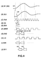
- the switching operation for the A/D converter 3, used in common for the routine compensation and adaptive compensation in the distortion compensation apparatus shown in Fig.3 is hereinafter explained. Specifically, such an operation is repeated in which the signal S25 causes selector switching, such that the case of digitizing the envelope of the input signal S1 and latching the digitized envelope as a signal S3 and the case of digitizing the envelope of the output S30 of the power amplifier 23 and latching the digitized envelope as the signal S24 are presented alternately.
- This allows to use a sole A/D converter for digitizing an input signal and for digitizing an output signal, thus reducing the size of the distortion compensation apparatus and achieving the saving in power consumption.
- the envelope signal S2 of the input signal S1 and the envelope signal S31 of the power amplifier 23 are switched in accordance with the timing of the signal S25 generated by the clock generator 24, at the same time as the digitized signals S22 (S24) and selector output signal S23 (S3) are latched.
- the random access memory 17 is read out with the rising edge of the clock MRW, obtained on frequency dividing the signal S25 in two, to produce a read-out signal S42, which is latched with the rising edge of the clocks LC.
- An address of the random access memory 17 at this time is a signal S3 obtained on digitizing the envelope S2 of the input signal S1.
- the clocks LC are obtained y the clock generator 24 delaying the clocks MRW.
- the readout signal S42 is latched by the first latch 18, at the same time as the third memory 19 starts to be accessed to read out the signal S44.
- This signal S44 is summed by the second addition unit 7 to the signal S7 to form a sum signal S9 and subsequently rendered into an analog signal S 10 at the first D/A converter 8 in timed relation to the decay of the clocks MRW and into an output signal S1 through the low-pass filter 9 the above operations are repeated within each period of the clocks MRW.
- Fig.5 shows typical data stored in the first memory 6.
- the abscissa and the ordinate indicate the voltage of an envelope signal S1 and the amplitude correction data converted in accordance with the equation (3).
- Fig.6 shows data stored in the second memory 10 and which allows for phase compensation.
- Fig.7 shows data stored in the third memory 19 and which has been linearly converted with respect to the positive and negative signs.
- Figs.8 and 9 indicate typical distortion compensation for 25°C (room temperature). Specifically, Figs. 8 and 9 show a spectrum containing distortion generated by the power amplifier 23 and a spectrum following distortion compensation by the second memory 10, respectively:
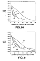
- Fig.11 shows the manner of adaptive compensation for +80°.
- the gain Cef as the parameter, is varied within a range of 0.5 to 1.25.
- characteristics 41 to 44 are obtained for the above parameter (gain Cef) of 0.5, 0.75, 1.0 and 1.25, respectively.
- Comparison with Fig.10 reveals that, since the gain of the power amplifier 23 is lowered for higher temperature, the loop gain of the feedback loop making up the adaptive amplitude distortion compensation is lowered thus increasing the number of times of integration required for deceasing the distortion power.
- an input high frequency signal Sin (S1) is sent via input terminal 31 to an anode terminal of a diode 32.
- An output signal Soo (S2) is derived from a cathode terminal connected to an output terminal 37.
- a parallel connection of a resistor 35 and a capacitor 36 is connected across the cathode terminal of the diode 32 and the ground. If high frequency signal Sin (S1) is fed to the input terminal 31, only the output signal Soo (S2) of the envelope component is presented at the output terminal 37.
- the diode 32 is fed with a bias voltage Vbias from a bias terminal 33 through a bias resistor 34.
- Fig.13 shows characteristics of the envelope voltage output signal Soo, obtained in the illustrative structure of Fig.10 , relative to the high frequency signal power applied as the input signal Sin.
- a dual gate FET 44 is used, with the circuit structure being of a source grounded type.
- the high frequency power to be controlled is input to the input terminal 45 to traverse an input matching circuit 46 so as to be input to the first gate G1 of the dual gate FET 44.
- To the drain D of the dual gate FET 44 is connected an output matching circuit 47 so that a controlled high frequency signal is output at an output terminal 48.
- a control voltage Vc is applied via a control terminal 41 to the second gate G2 of the dual gate FET 44 connected to a resistor 42 and a capacitor 43.
- the mutual conductance of the dual gate FET 44 which depends on the voltage applied to te second gate G2, is used to control the gain.
- Fig.15 shows another specified embodiment of the gain changing unit 22 employing a gate grounded FET 52.
- terminals 51, 53 represent a source and a drain of the FET 52 and a path for high frequency signals.
- a control voltage is applied from a terminal 54 to adjust the passage loss.
- a capacitor 56 is connected across the gate and the ground.
- the gain changing unit 22 is desirably so designed that the passage phase is not fluctuated with gain fluctuations.
- the circuits of Figs. 14 and 15 both satisfy this requirement.
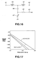
- Fig.16 shows a specified embodiment of the phase shifter 21 in which terminals 61, 62 are input/output terminals across which coils 64, 65 are connected in series.
- a capacitor 66 and a variable capacitance 67 such as a VARICAP diode, are connected in series to a junction of the two coils 64, 64 and connected to the ground, and a control terminal 63 is provided through a resistor 68 to a junction between the capacitor 66 and the variable capacitance 67.
- the high frequency signal traversing the terminals 61, 62 can be shifted in phase by a voltage Vctl applied to the control terminal 63.
- Fig.17 shows typical characteristics of the phase shifter 21 in case the capacitor 66, resistor 68 and the coils 64, 65 are set to 2.5 pF, 1 k ⁇ , 5 nH and 5 nH, respectively.
- the phase shift of 10° to 40° takes place generally in a range from 0.5V to 3.0 V, depending on the frequency.
- adaptive compensation data required for pre-distortion can be realized extremely readily without requiring orthogonal demodulation because the distortion components of the power amplifier 23 are enabled by using the method of envelope detection. Since the distortion component is detected by integration of the output and the input difference to effect distortion compensation, the slightest distortion component can be advantageously compensated. Moreover, since the A/D converter is used in a switching fashion between rotine compensation and adaptive compensation, only one A/D converter suffices, so that small size and low power consumption may advantageously be achieved.
- the distortion compensation apparatus includes adaptive phase distortion compensation means which outputs adaptive correction data for the phase distortion against temperature changes of the power amplifier, based on the phase difference between the input signal supplied to the power amplifier and the output signals of the power amplifier, and effects adaptive compensation of phase distortion of the power amplifier using the adaptive correction data.
- a distortion compensation apparatus shown in Fig.18 , includes a phase difference detector (DP) 71, fed with an input signal S1 and an output signal S30 of the power amplifier 23 to output the phase difference therebetween as a voltage S100, a memory (MP) 72 for outputting, as signal S 101, data having an output of the phase difference detector 71 as an address, and an adder 73 fed with an output of the memory 72 and summing the output of the second memory 10 to the output of the memory 72.
- a sum output of the adder 73 is routed to the second D/A converter 11.
- phase difference detector 71 If the data of the second memory 10, as a table for phase compensation, is proper, no output appears in the phase difference detector 71 so that no operation occurs. If the data is not proper, a voltage S100 dependent on the phase different of the input/output signal of the power amplifier 23 is generated. In the memory 72, data similar to that in the random access memory 17 is stored and data conversion dependent on the signal S100 is executed to produce a signal S101. This signal S 101 is summed to the output S4 of the phase compensation table (second memory 10) to contribute to the control of the phase shifter 21.
- Fig.19 shows a specified embodiment of the phase difference detector 71.
- a series connection of a resistor 93 and a capacitor 94 and another series connection of a capacitor 95 and a resistor 96 are connected in parallel to make up a bridge. If two signals (S1, S30), the phase difference of which is to be measured, are input to two opposite input terminals 91, 92 of the bridge, there is produced a voltage corresponding to the phase difference across the other two opposite terminals of the bridge.
- To these terminals are connected two square detection circuits, made up of diodes 97, 100, resistors 98, 101 and capacitors 99, 102, with the outputs of these square detection circuits being fed to a subtractor.
- This subtractor is comprised of an operational amplifier 107, an inverting terminal (-) of which is fed via a resistor 103 with an output of the first square detection circuit made up of the diode 97, resistor 98 and the capacitor 99, and a positive terminal (+) of which is fed via a resistor 105 with an output of the second square detection circuit made up of the diode 100, resistor 101 and the capacitor 102.
- a resistor 104 is connected across the inverting terminal (-) of the operational amplifier 107, whilst a resistor 106 is connected between the positive terminal (+) and the ground.
Landscapes
- Physics & Mathematics (AREA)
- Nonlinear Science (AREA)
- Engineering & Computer Science (AREA)
- Power Engineering (AREA)
- Amplifiers (AREA)
- Transmitters (AREA)
Claims (15)
- Verzerrungskompensationsvorrichtung zum Kompensieren von Verzerrungskomponenten, welche in einer Einrichtung (23) erzeugt werden, welche umfasst:eine adaptive Amplitudenverzerrungs-Kompensationseinrichtung zum Finden einer Amplitudendifferenz (S40) zwischen einem Hüllkurvensignal (S2) eines Eingangssignals (S1), welches der Einrichtung (23) zugeführt wird, und einem Hüllkurvensignal (S31) eines Ausgangssignals der Einrichtung (23), Ausgeben adaptiver Korrekturdaten (S44) der Amplitudenverzerrung gegenüber Temperaturschwankungen in der Einrichtung (23), und zum adaptiven Kompensieren der Amplitudenverzerrung (S40) der Einrichtung (23) unter Verwendung der adaptiven Korrekturdaten (S44), wobei die adaptive Amplitudenverzerrungs-Kompensationseinrichtung eine erste Hüllkurvenerfassungseinrichtung (1) aufweist, um ein Hüllkurvensignal (S2) eines Eingangssignals (S1) zu erfassen, welches zur Einrichtung (23) geliefert wird, eine zweite Hüllkurvenerfassungseinrichtung (13), um die Hüllkurvenkomponente (S31) eines Ausgangssignals (S30) der Einrichtung (23) zu erfassen, und eine Subtraktionseinrichtung (15), um eine Amplitudendifferenz (S40) zwischen der Hüllkurvenkomponente (S2) des Eingangssignals (S1), wenn durch die erste Hüllkurvenerfassungseinrichtung (19 erfasst, und der Hüllkurvenkomponente (S31) des Ausgangssignals (S30), wenn durch die zweite Hüllkurvenerfassungseinrichtung (13) erfasst, zu finden, dadurch gekennzeichnet, dass diese außerdem aufweist:eine Kumulationseinrichtung (16, 17, 18) zum Integrieren und Kumulieren der Amplitudendifferenz (S40), wenn durch die Subtraktionseinrichtung (15) erlangt, und eine adaptive Korrekturdaten-Ausgabeeinrichtung (19) zum Ausgeben der adaptiven Korrekturdaten (S44) auf Basis der kumulierten Ergebnisse der Kumulationseinrichtung (16, 17, 18), wobeidie Kumulationseinrichtung (16, 17, 18) einen Addierer (16), einen Speicher mit wahlfreiem Zugriff (17) und eine Latch-Schaltung (18) umfasst, wobei der Addierer (16) konfiguriert ist, ein Ausgangssignal von der Latch-Schaltung (18) mit einem Ausgangssignal von der Subtraktionseinrichtung (15) zu addieren und die Summe an den Speicher (17) mit wahlfreiem Zugriff auszugeben, um bei einer Adresse (S3) in den Speicher (17) mit wahlfreiem Zugriff entsprechend einer digitalisierten Darstellung des Hüllkurvensignals (S2) des Eingangssignals (S1) zu schreiben, und die Latch-Schaltung (18) konfiguriert ist, ein Ausgangssignal (S42) von dem Speicher (17) mit wahlfreiem Zugriff zu verriegeln; unddie adaptive Korrekturdaten-Ausgangseinrichtung (19) einen Speicher (19) aufweist, der konfiguriert ist, die adaptiven Korrekturdaten (S44) unter Verwendung des Signals (S43), welches durch die Latch-Schaltung (18) ausgegeben wird, als eine Adresse auszugeben.
- Verzerrungskompensationsvorrichtung nach Anspruch 1, welche außerdem aufweist:eine Amplitudenverzerrungs-Korrektureinrichtung zum Ausgeben von Korrekturdaten zum Korrigieren der Amplitudenverzerrung der Einrichtung (23) auf Basis des Hüllkurvensignal (S2) des Eingangssignals (S1), welches zur Einrichtung (23) geliefert wird, und zum Steuern des Verstärkungsfaktor-Änderungsverarbeitung der Einrichtung (23), als Antwort auf die Korrekturdaten, um die Amplitudenverzerrung der Einrichtung (23) zu korrigieren.
- Verzerrungskompensationsvorrichtung nach Anspruch 2, wobei die adaptive Amplitudenverzerrungs-Kompensationseinrichtung konfiguriert ist, die adaptiven Korrekturdaten (S44) mit den Korrekturdaten zu addieren, welche in der Amplitudenverzerrungs-Korrektureinrichtung verwendet werden, um adaptive Kompensation der Amplitudenverzerrung der Einrichtung (23) zu bewirken.
- Verzerrungskompensationsvorrichtung nach einem der vorhergehenden Ansprüche, welche außerdem umfasst:eine adaptive Phasenverzerrungs-Kompensationseinrichtung, um adaptive Phasenverzerrungs-Korrekturdaten (S4) gegenüber Temperaturschwankungen der Einrichtung (23) auszugeben, auf Basis einer Phasendifferenz zwischen einem Eingangssignal (S1), welches zur Einrichtung (23) geliefert wird, und eines Ausgangssignals (S30) von der Einrichtung (23), und zum adaptiven Kompensieren der Phasenverzerrung der Einrichtung (23) unter Verwendung der adaptiven Korrekturdaten.
- Verzerrungskompensationsvorrichtung nach Anspruch 4, welche außerdem umfasst:eine Phasenverzerrungs-Korrektureinrichtung zum Ausgeben von Korrekturdaten zum Korrigieren der Phasenverzerrung der Einrichtung (23) auf Basis eines Hüllkurvensignals (S2) eines Eingangssignals (S1), welches zur Einrichtung (23) geliefert wird, und zum Steuern der Phasenverschiebungsverarbeitung der Einrichtung (23) als Antwort auf die Korrekturdaten, um die Phasenverzerrung der Einrichtung (23) zu korrigieren.
- Verzerrungskompensationsvorrichtung nach Anspruch 5, wobei die adaptive Phasenverzerrungs-Kompensationseinrichtung konfiguriert ist, die adaptiven Korrekturdaten (S4) mit den Korrekturdaten, welche bei der Phasenverzerrung verwendet werden, zu addieren, welche umfasst:eine Korrektureinrichtung zum adaptiven Kompensieren der Phasenverzerrung der Einrichtung (23).
- Verzerrungskompensationsvorrichtung nach Anspruch 4, 5 oder 6, wobei die adaptive Phasenverzerrungs-Kompensationseinrichtung eine Phasendifferenz-Erfassungseinrichtung (71) aufweist, um die Phasendifferenz zwischen einem Eingangssignal (S1), welches zur Einrichtung (23) geliefert wird, und einem Ausgangssignal (S30) von der Einrichtung (23) zu erfassen, und eine adaptive Phasenverzerrungs-Korrekturdaten-Ausgabeeinrichtung, um adaptive Phasenverzerrungs-Korrekturdaten gegenüber Temperaturschwankungen der Einrichtung (23) auf Basis der Phasendifferenz auszugeben, wie durch die Phasendifferenz-Erfassungseinrichtung (71) erfasst.
- Verzerrungskompensationsvorrichtung nach einem der vorhergehenden Ansprüche, wobei die Einrichtung (23) eine Spannungsverstärkungseinrichtung ist, und das Eingangssignal (S1) ein Hochfrequenz-Eingangssignal ist, welches Hüllkurvenschwankungen unterworfen ist.
- Verzerrungskompensationsverfahren zum Kompensieren von Verzerrungskomponenten, welche in einer Einrichtung (23) erzeugt werden, welches umfasst:einen adaptiven Amplitudenverzerrungs-Kompensationsschritt zum Finden einer Amplitudendifferenz (S40) zwischen einem Hüllkurvensignal (S2) eines Eingangssignals (S1), welches zur Einrichtung (23) geliefert wird, und einem Hüllkurvensignal (S31) eines Ausgangssignals (S30) der Einrichtung (23), zum Ausgeben adaptiver Korrekturdaten der Amplitudenverzerrung gegenüber Temperaturschwankungen in der Einrichtung (23) und zum adaptiven Kompensieren der Amplitudenverzerrung der Einrichtung (23) unter Verwendung der adaptiven Korrekturdaten, wobei der adaptive Amplitudenverzerrungs-Kompensationsschritt das Erfassen eines Hüllkurvensignals (S2) eines Eingangssignals (S1) umfasst, welches zur Einrichtung (23) geliefert wird, das Erfassen der Hüllkurvenkomponente (S31) eines Ausgangssignals der Einrichtung (23), und das Finden einer Amplitudendifferenz (S40) zwischen der Hüllkurvenkomponente (S2) des Eingangssignals (S1), wie erfasst, und der Hüllkurvenkomponente (S31) des Ausgangssignals (S30), wie erfasst, dadurch gekennzeichnet, dassder adaptive Amplitudenverzerrungs-Kompensationsschritt außerdem das Integrieren und Kumulieren der Amplitudendifferenz (S40) und das Ausgeben der adaptiven Korrekturdaten (S44) auf Basis der Ergebnisse des Integrierens und des Kumulierens umfasst, wobeidas Integrieren und Kumulieren unter Verwendung einer Kumulationseinrichtung (16, 17, 18) ausgeführt wird, welche einen Addierer (16), einen Speicher (17) mit wahlfreiem Zugriff und eine Latch-Schaltung (18) umfasst, wobei der Addierer (16) konfiguriert ist, ein Ausgangssignal von der Latch-Schaltung (18) mit einem Ausgangssignal von der Subtraktionseinrichtung (15) zu addieren, welches verwendet wird, die Amplitudendifferenz (S40) zu erlangen und um die Summe an den Speicher (17) mit wahlfreiem Zugriff auszugeben, um bei einer Adresse (S3) in den Speicher (17) mit wahlfreiem Zugriff entsprechend einer digitalisierten Darstellung der Hüllkurvenkomponente (S2) des Eingangssignals (S1) zu schreiben, und die Latch-Schaltung (18) konfiguriert ist, ein Ausgangssignal (S42) vom Speicher (17) mit wahlfreiem Zugriff zu verriegeln; unddie adaptiven Korrekturdaten (S44) von einem Speicher (19) unter Verwendung des Signals (S43), welches durch die Latch-Schaltung (18) ausgegeben wird, als eine Adresse ausgegeben werden.
- Verzerrungskompensationsverfahren nach Anspruch 9, welches außerdem umfasst:einem Amplitudenverzerrungs-Korrekturschritt zum Ausgeben von Korrekturdaten zum Korrigieren der Amplitudenverzerrung der Einrichtung (23) auf Basis des Hüllkurvensignals (S2) des Eingangssignals (S1), welches zur Einrichtung (23) geliefert wird, und zum Steuern der Verstärkungsfaktor-Änderungsverarbeitung der Einrichtung (23) als Antwort auf die Korrekturdaten, um die Amplitudenverzerrung der Einrichtung (23) zu korrigieren.
- Verzerrungskompensationsverfahren nach Anspruch 10, wobei der adaptive Amplitudenverzerrungs-Kompensationsschritt die adaptiven Korrekturdaten (S44) mit den Korrekturdaten addiert, welche in dem Amplitudenverzerrungs-Korrekturschritt verwendet werden, um adaptive Kompensation der Amplitudenverzerrung der Einrichtung (23) zu bewirken.
- Verzerrungskompensationsverfahren nach Anspruch 9, 10 oder 11, welches außerdem umfasst:einen adaptiven Phasenverzerrungs-Kompensationsschritt zum Ausgeben von adaptiven Phasenverzerrungs-Korrekturdaten (S44) gegenüber Temperaturschwankungen der Einrichtung (23) auf Basis einer Phasendifferenz zwischen einem Eingangssignal (S1), welches zur Einrichtung (23) geliefert wird, und einem Ausgangssignal (S30) von der Einrichtung (23), und zum adaptiven Kompensieren der Phasenverzerrung der Einrichtung (23) unter Verwendung der adaptiven Korrekturdaten.
- Verzerrungskompensationsverfahren nach Anspruch 12, welches außerdem umfasst:einen Phasenverzerrungs-Korrekturschritt zum Ausgeben von Korrekturdaten zum Korrigieren der Phasenverzerrung der Einrichtung (23) auf Basis eines Hüllkurvensignals eines Eingangssignals (S1), welches zur Einrichtung (23) geliefert wird, und zum Steuern der Phasenverschiebungsverarbeitung der Einrichtung (23) als Antwort auf die Korrekturdaten, um die Phasenverzerrung der Einrichtung (23) zu korrigieren.
- Verzerrungskompensationsverfahren nach Anspruch 13, wobei der adaptive Phasenverzerrungs-Kompensationsschritt die adaptiven Korrekturdaten (S44) mit den Korrekturdaten addiert, welche im Phasenverzerrungs-Korrekturschritt verwendet werden, um die Phasenverzerrung der Einrichtung (23) adaptiv zu kompensieren.
- Verzerrungskompensationsverfahren nach einem der Ansprüche 9 bis 14, wobei die Einrichtung (23) eine Leistungsverstärkungseinrichtung ist, und das Eingangssignal (S1) ein Hochfrequenz-Eingangssignal ist, welches Hüllkurvenschwankungen unterworfen ist.
Applications Claiming Priority (2)
| Application Number | Priority Date | Filing Date | Title |
|---|---|---|---|
| JP2000182274A JP2002009556A (ja) | 2000-06-16 | 2000-06-16 | 歪補償装置及び歪補償方法 |
| JP2000182274 | 2000-06-16 |
Publications (3)
| Publication Number | Publication Date |
|---|---|
| EP1170859A2 EP1170859A2 (de) | 2002-01-09 |
| EP1170859A3 EP1170859A3 (de) | 2005-02-09 |
| EP1170859B1 true EP1170859B1 (de) | 2009-05-06 |
Family
ID=18683067
Family Applications (1)
| Application Number | Title | Priority Date | Filing Date |
|---|---|---|---|
| EP01305186A Expired - Lifetime EP1170859B1 (de) | 2000-06-16 | 2001-06-14 | Verzerrungsausgleichverfahren und Gerät |
Country Status (6)
| Country | Link |
|---|---|
| US (1) | US6466092B2 (de) |
| EP (1) | EP1170859B1 (de) |
| JP (1) | JP2002009556A (de) |
| KR (1) | KR100872505B1 (de) |
| CN (1) | CN1225833C (de) |
| DE (1) | DE60138593D1 (de) |
Families Citing this family (14)
| Publication number | Priority date | Publication date | Assignee | Title |
|---|---|---|---|---|
| JP3740379B2 (ja) * | 2000-04-19 | 2006-02-01 | キヤノン株式会社 | 画像処理装置及び画像処理方法 |
| US7315388B2 (en) | 2001-01-24 | 2008-01-01 | Canon Kabushiki Kaisha | Image input/output control apparatus, image processing apparatus, image processing method, data communication apparatus, and data communication method |
| US6600374B2 (en) * | 2001-06-25 | 2003-07-29 | Rambus Inc. | Collective automatic gain control |
| KR100448892B1 (ko) * | 2002-06-04 | 2004-09-18 | 한국전자통신연구원 | 고전력 증폭기의 비선형 왜곡 보상을 위한 전치 왜곡 장치및 그 방법 |
| JP4175503B2 (ja) * | 2003-04-18 | 2008-11-05 | ソニー・エリクソン・モバイルコミュニケーションズ株式会社 | 歪み補償回路及び送信装置 |
| CN101023578B (zh) * | 2004-09-21 | 2010-04-21 | 株式会社日立国际电气 | 失真补偿放大装置 |
| JP4617265B2 (ja) * | 2006-02-14 | 2011-01-19 | 富士通株式会社 | 歪補償装置及び歪補償方法 |
| US7856105B2 (en) * | 2006-03-09 | 2010-12-21 | Andrew Llc | Apparatus and method for processing of amplifier linearization signals |
| US20070295555A1 (en) * | 2006-06-26 | 2007-12-27 | The United States Of America As Represented By The Secretary Of The Navy | Hoisting harness assembly |
| JP4757231B2 (ja) * | 2007-06-01 | 2011-08-24 | 富士通株式会社 | 送信装置 |
| JP2010154042A (ja) | 2008-12-24 | 2010-07-08 | Sumitomo Electric Ind Ltd | 歪補償回路 |
| JP4951074B2 (ja) * | 2010-02-26 | 2012-06-13 | 株式会社エヌ・ティ・ティ・ドコモ | べき級数型ディジタルプリディストータとその歪補償制御方法 |
| KR101977783B1 (ko) * | 2017-10-17 | 2019-05-13 | 주식회사 케이엠더블유 | 전력 증폭기 성능 보정 방법 및 그를 위한 장치 |
| JP7667755B2 (ja) * | 2022-02-22 | 2025-04-23 | 株式会社国際電気 | 増幅装置、無線装置、及び監視方法 |
Family Cites Families (7)
| Publication number | Priority date | Publication date | Assignee | Title |
|---|---|---|---|---|
| US4210874A (en) * | 1978-10-23 | 1980-07-01 | Raytheon Company | Gain control amplifier circuit |
| US4389618A (en) * | 1981-04-15 | 1983-06-21 | The United States Of America As Represented By The Secretary Of The Navy | Adaptive feed-forward system |
| US4591800A (en) * | 1984-10-01 | 1986-05-27 | Motorola, Inc. | Linear power amplifier feedback improvement |
| JPH0771118B2 (ja) * | 1989-12-27 | 1995-07-31 | 三菱電機株式会社 | 変調装置 |
| US5105164A (en) * | 1989-02-28 | 1992-04-14 | At&T Bell Laboratories | High efficiency uhf linear power amplifier |
| GB9002788D0 (en) * | 1990-02-08 | 1990-04-04 | Marconi Co Ltd | Circuit for reducing distortion produced by an r.f.power amplifier |
| US6275685B1 (en) * | 1998-12-10 | 2001-08-14 | Nortel Networks Limited | Linear amplifier arrangement |
-
2000
- 2000-06-16 JP JP2000182274A patent/JP2002009556A/ja not_active Abandoned
-
2001
- 2001-06-14 EP EP01305186A patent/EP1170859B1/de not_active Expired - Lifetime
- 2001-06-14 DE DE60138593T patent/DE60138593D1/de not_active Expired - Fee Related
- 2001-06-14 KR KR1020010033524A patent/KR100872505B1/ko not_active Expired - Fee Related
- 2001-06-15 US US09/882,224 patent/US6466092B2/en not_active Expired - Fee Related
- 2001-06-15 CN CNB011243392A patent/CN1225833C/zh not_active Expired - Fee Related
Also Published As
| Publication number | Publication date |
|---|---|
| KR20010113494A (ko) | 2001-12-28 |
| EP1170859A3 (de) | 2005-02-09 |
| EP1170859A2 (de) | 2002-01-09 |
| US6466092B2 (en) | 2002-10-15 |
| DE60138593D1 (de) | 2009-06-18 |
| JP2002009556A (ja) | 2002-01-11 |
| CN1340911A (zh) | 2002-03-20 |
| KR100872505B1 (ko) | 2008-12-08 |
| US20020010567A1 (en) | 2002-01-24 |
| CN1225833C (zh) | 2005-11-02 |
Similar Documents
| Publication | Publication Date | Title |
|---|---|---|
| US11159129B2 (en) | Power amplifier time-delay invariant predistortion methods and apparatus | |
| US6373902B1 (en) | Device and method for linearizing transmitter in digital communication system | |
| EP0881807B1 (de) | Sender mit linearisiertem Verstärker | |
| KR100325051B1 (ko) | 프리디스토터 | |
| EP1193865B1 (de) | Verzerrungsskompensationseinrichtung und Verfahren | |
| KR20020019466A (ko) | 왜곡보상장치 | |
| US6466092B2 (en) | Distortion compensation method and apparatus | |
| EP1252709B1 (de) | Verfahren und vorrichtung zum kompensieren von nicht-linearitäten und zeitvarianten änderungen einer übertragungsfunktion wirksam auf ein eingangssignal | |
| US6766151B2 (en) | Distortion-compensating apparatus | |
| US6452447B2 (en) | Adaptive distortion-compensation apparatus | |
| JPH0531326B2 (de) | ||
| JP4243526B2 (ja) | 送信電力制御方法及び装置 | |
| KR100417413B1 (ko) | 디지탈 선형화기 | |
| KR100469408B1 (ko) | Cdma 시스템의 선형 증폭 장치 및 방법 | |
| KR100414075B1 (ko) | Aqm의 에러보상장치 및 방법 |
Legal Events
| Date | Code | Title | Description |
|---|---|---|---|
| PUAI | Public reference made under article 153(3) epc to a published international application that has entered the european phase |
Free format text: ORIGINAL CODE: 0009012 |
|
| AK | Designated contracting states |
Kind code of ref document: A2 Designated state(s): AT BE CH CY DE DK ES FI FR GB GR IE IT LI LU MC NL PT SE TR |
|
| AX | Request for extension of the european patent |
Free format text: AL;LT;LV;MK;RO;SI |
|
| PUAL | Search report despatched |
Free format text: ORIGINAL CODE: 0009013 |
|
| AK | Designated contracting states |
Kind code of ref document: A3 Designated state(s): AT BE CH CY DE DK ES FI FR GB GR IE IT LI LU MC NL PT SE TR |
|
| AX | Request for extension of the european patent |
Extension state: AL LT LV MK RO SI |
|
| 17P | Request for examination filed |
Effective date: 20050712 |
|
| AKX | Designation fees paid |
Designated state(s): DE FR GB |
|
| 17Q | First examination report despatched |
Effective date: 20080318 |
|
| GRAP | Despatch of communication of intention to grant a patent |
Free format text: ORIGINAL CODE: EPIDOSNIGR1 |
|
| GRAS | Grant fee paid |
Free format text: ORIGINAL CODE: EPIDOSNIGR3 |
|
| GRAA | (expected) grant |
Free format text: ORIGINAL CODE: 0009210 |
|
| RAP1 | Party data changed (applicant data changed or rights of an application transferred) |
Owner name: SONY CORPORATION |
|
| AK | Designated contracting states |
Kind code of ref document: B1 Designated state(s): DE FR GB |
|
| REG | Reference to a national code |
Ref country code: GB Ref legal event code: FG4D |
|
| REF | Corresponds to: |
Ref document number: 60138593 Country of ref document: DE Date of ref document: 20090618 Kind code of ref document: P |
|
| PGFP | Annual fee paid to national office [announced via postgrant information from national office to epo] |
Ref country code: DE Payment date: 20090615 Year of fee payment: 9 |
|
| PLBE | No opposition filed within time limit |
Free format text: ORIGINAL CODE: 0009261 |
|
| STAA | Information on the status of an ep patent application or granted ep patent |
Free format text: STATUS: NO OPPOSITION FILED WITHIN TIME LIMIT |
|
| 26N | No opposition filed |
Effective date: 20100209 |
|
| GBPC | Gb: european patent ceased through non-payment of renewal fee |
Effective date: 20090806 |
|
| PG25 | Lapsed in a contracting state [announced via postgrant information from national office to epo] |
Ref country code: GB Free format text: LAPSE BECAUSE OF NON-PAYMENT OF DUE FEES Effective date: 20090806 |
|
| REG | Reference to a national code |
Ref country code: FR Ref legal event code: ST Effective date: 20110228 |
|
| PG25 | Lapsed in a contracting state [announced via postgrant information from national office to epo] |
Ref country code: DE Free format text: LAPSE BECAUSE OF NON-PAYMENT OF DUE FEES Effective date: 20110101 |
|
| PG25 | Lapsed in a contracting state [announced via postgrant information from national office to epo] |
Ref country code: FR Free format text: LAPSE BECAUSE OF NON-PAYMENT OF DUE FEES Effective date: 20100630 |
|
| PGFP | Annual fee paid to national office [announced via postgrant information from national office to epo] |
Ref country code: FR Payment date: 20090611 Year of fee payment: 9 |