EP1172760B1 - Bobine d'antenne pour carte à puce et méthode de fabrication - Google Patents
Bobine d'antenne pour carte à puce et méthode de fabrication Download PDFInfo
- Publication number
- EP1172760B1 EP1172760B1 EP01115099A EP01115099A EP1172760B1 EP 1172760 B1 EP1172760 B1 EP 1172760B1 EP 01115099 A EP01115099 A EP 01115099A EP 01115099 A EP01115099 A EP 01115099A EP 1172760 B1 EP1172760 B1 EP 1172760B1
- Authority
- EP
- European Patent Office
- Prior art keywords
- circuit pattern
- base material
- antenna coil
- pattern layer
- mass
- Prior art date
- Legal status (The legal status is an assumption and is not a legal conclusion. Google has not performed a legal analysis and makes no representation as to the accuracy of the status listed.)
- Expired - Lifetime
Links
Images




Classifications
-
- G—PHYSICS
- G06—COMPUTING OR CALCULATING; COUNTING
- G06K—GRAPHICAL DATA READING; PRESENTATION OF DATA; RECORD CARRIERS; HANDLING RECORD CARRIERS
- G06K19/00—Record carriers for use with machines and with at least a part designed to carry digital markings
- G06K19/06—Record carriers for use with machines and with at least a part designed to carry digital markings characterised by the kind of the digital marking, e.g. shape, nature, code
- G06K19/067—Record carriers with conductive marks, printed circuits or semiconductor circuit elements, e.g. credit or identity cards also with resonating or responding marks without active components
- G06K19/07—Record carriers with conductive marks, printed circuits or semiconductor circuit elements, e.g. credit or identity cards also with resonating or responding marks without active components with integrated circuit chips
- G06K19/077—Constructional details, e.g. mounting of circuits in the carrier
- G06K19/07749—Constructional details, e.g. mounting of circuits in the carrier the record carrier being capable of non-contact communication, e.g. constructional details of the antenna of a non-contact smart card
- G06K19/07773—Antenna details
- G06K19/07777—Antenna details the antenna being of the inductive type
- G06K19/07779—Antenna details the antenna being of the inductive type the inductive antenna being a coil
-
- G—PHYSICS
- G06—COMPUTING OR CALCULATING; COUNTING
- G06K—GRAPHICAL DATA READING; PRESENTATION OF DATA; RECORD CARRIERS; HANDLING RECORD CARRIERS
- G06K19/00—Record carriers for use with machines and with at least a part designed to carry digital markings
- G06K19/06—Record carriers for use with machines and with at least a part designed to carry digital markings characterised by the kind of the digital marking, e.g. shape, nature, code
- G06K19/067—Record carriers with conductive marks, printed circuits or semiconductor circuit elements, e.g. credit or identity cards also with resonating or responding marks without active components
- G06K19/07—Record carriers with conductive marks, printed circuits or semiconductor circuit elements, e.g. credit or identity cards also with resonating or responding marks without active components with integrated circuit chips
- G06K19/0723—Record carriers with conductive marks, printed circuits or semiconductor circuit elements, e.g. credit or identity cards also with resonating or responding marks without active components with integrated circuit chips the record carrier comprising an arrangement for non-contact communication, e.g. wireless communication circuits on transponder cards, non-contact smart cards or RFIDs
-
- G—PHYSICS
- G06—COMPUTING OR CALCULATING; COUNTING
- G06K—GRAPHICAL DATA READING; PRESENTATION OF DATA; RECORD CARRIERS; HANDLING RECORD CARRIERS
- G06K19/00—Record carriers for use with machines and with at least a part designed to carry digital markings
- G06K19/06—Record carriers for use with machines and with at least a part designed to carry digital markings characterised by the kind of the digital marking, e.g. shape, nature, code
- G06K19/067—Record carriers with conductive marks, printed circuits or semiconductor circuit elements, e.g. credit or identity cards also with resonating or responding marks without active components
- G06K19/07—Record carriers with conductive marks, printed circuits or semiconductor circuit elements, e.g. credit or identity cards also with resonating or responding marks without active components with integrated circuit chips
- G06K19/077—Constructional details, e.g. mounting of circuits in the carrier
- G06K19/07749—Constructional details, e.g. mounting of circuits in the carrier the record carrier being capable of non-contact communication, e.g. constructional details of the antenna of a non-contact smart card
-
- G—PHYSICS
- G06—COMPUTING OR CALCULATING; COUNTING
- G06K—GRAPHICAL DATA READING; PRESENTATION OF DATA; RECORD CARRIERS; HANDLING RECORD CARRIERS
- G06K19/00—Record carriers for use with machines and with at least a part designed to carry digital markings
- G06K19/06—Record carriers for use with machines and with at least a part designed to carry digital markings characterised by the kind of the digital marking, e.g. shape, nature, code
- G06K19/067—Record carriers with conductive marks, printed circuits or semiconductor circuit elements, e.g. credit or identity cards also with resonating or responding marks without active components
- G06K19/07—Record carriers with conductive marks, printed circuits or semiconductor circuit elements, e.g. credit or identity cards also with resonating or responding marks without active components with integrated circuit chips
- G06K19/077—Constructional details, e.g. mounting of circuits in the carrier
- G06K19/07749—Constructional details, e.g. mounting of circuits in the carrier the record carrier being capable of non-contact communication, e.g. constructional details of the antenna of a non-contact smart card
- G06K19/07773—Antenna details
- G06K19/07777—Antenna details the antenna being of the inductive type
- G06K19/07779—Antenna details the antenna being of the inductive type the inductive antenna being a coil
- G06K19/07783—Antenna details the antenna being of the inductive type the inductive antenna being a coil the coil being planar
-
- G—PHYSICS
- G06—COMPUTING OR CALCULATING; COUNTING
- G06K—GRAPHICAL DATA READING; PRESENTATION OF DATA; RECORD CARRIERS; HANDLING RECORD CARRIERS
- G06K19/00—Record carriers for use with machines and with at least a part designed to carry digital markings
- G06K19/06—Record carriers for use with machines and with at least a part designed to carry digital markings characterised by the kind of the digital marking, e.g. shape, nature, code
- G06K19/067—Record carriers with conductive marks, printed circuits or semiconductor circuit elements, e.g. credit or identity cards also with resonating or responding marks without active components
- G06K19/07—Record carriers with conductive marks, printed circuits or semiconductor circuit elements, e.g. credit or identity cards also with resonating or responding marks without active components with integrated circuit chips
- G06K19/077—Constructional details, e.g. mounting of circuits in the carrier
- G06K19/07749—Constructional details, e.g. mounting of circuits in the carrier the record carrier being capable of non-contact communication, e.g. constructional details of the antenna of a non-contact smart card
- G06K19/07773—Antenna details
- G06K19/07777—Antenna details the antenna being of the inductive type
- G06K19/07784—Antenna details the antenna being of the inductive type the inductive antenna consisting of a plurality of coils stacked on top of one another
-
- H—ELECTRICITY
- H05—ELECTRIC TECHNIQUES NOT OTHERWISE PROVIDED FOR
- H05K—PRINTED CIRCUITS; CASINGS OR CONSTRUCTIONAL DETAILS OF ELECTRIC APPARATUS; MANUFACTURE OF ASSEMBLAGES OF ELECTRICAL COMPONENTS
- H05K1/00—Printed circuits
- H05K1/02—Details
- H05K1/09—Use of materials for the conductive, e.g. metallic pattern
-
- H—ELECTRICITY
- H05—ELECTRIC TECHNIQUES NOT OTHERWISE PROVIDED FOR
- H05K—PRINTED CIRCUITS; CASINGS OR CONSTRUCTIONAL DETAILS OF ELECTRIC APPARATUS; MANUFACTURE OF ASSEMBLAGES OF ELECTRICAL COMPONENTS
- H05K3/00—Apparatus or processes for manufacturing printed circuits
- H05K3/38—Improvement of the adhesion between the insulating substrate and the metal
- H05K3/386—Improvement of the adhesion between the insulating substrate and the metal by the use of an organic polymeric bonding layer, e.g. adhesive
-
- H—ELECTRICITY
- H05—ELECTRIC TECHNIQUES NOT OTHERWISE PROVIDED FOR
- H05K—PRINTED CIRCUITS; CASINGS OR CONSTRUCTIONAL DETAILS OF ELECTRIC APPARATUS; MANUFACTURE OF ASSEMBLAGES OF ELECTRICAL COMPONENTS
- H05K2201/00—Indexing scheme relating to printed circuits covered by H05K1/00
- H05K2201/01—Dielectrics
- H05K2201/0183—Dielectric layers
- H05K2201/0195—Dielectric or adhesive layers comprising a plurality of layers, e.g. in a multilayer structure
-
- H—ELECTRICITY
- H05—ELECTRIC TECHNIQUES NOT OTHERWISE PROVIDED FOR
- H05K—PRINTED CIRCUITS; CASINGS OR CONSTRUCTIONAL DETAILS OF ELECTRIC APPARATUS; MANUFACTURE OF ASSEMBLAGES OF ELECTRICAL COMPONENTS
- H05K2201/00—Indexing scheme relating to printed circuits covered by H05K1/00
- H05K2201/03—Conductive materials
- H05K2201/0332—Structure of the conductor
- H05K2201/0335—Layered conductors or foils
- H05K2201/0355—Metal foils
Definitions
- the present invention relates to an antenna coil for an IC card and to the method of manufacturing the same. More specifically, the present invention relates to an antenna coil for an IC card in which a circuit pattern layer of the antenna coil for the IC card is formed of an aluminum foil, as well as to the method of manufacturing the same.
- the aluminum foil is not limited to a pure aluminum foil but it also includes an aluminum alloy foil.
- IC cards have been developed remarkably, and the use of the IC cards is widening to telephone cards, credit cards, pre-paid cards, cash cards, ID cards and card keys.
- resin film such as a polyimide film, a general purpose polyethylene terephthalate (PET) film or the like has been used.
- PET polyethylene terephthalate
- a copper foil or a high-purity aluminum foil is laminated on each side of the resin film and subjected to etching, whereby a circuit pattern layer of copper or aluminum is formed on a surface of the base material, providing an antenna coil for the IC card.
- the process of etching the copper foil for forming the circuit pattern layer takes too much time, and therefore production efficiency is low. Further, after the etching process of the copper foil, an oxidizing reaction tends to occur at the surface of the copper foil, making instable the electrical resistance value of the surface of the circuit pattern.
- a high-purity aluminum foil (having the purity of at least 99.8 mass %) is used as the material for forming the circuit pattern layer, superior oxidation resistance can be attained. Etching, however, takes longer time, resulting in low production efficiency.
- An IC card having the circuit pattern layer formed by using the high-purity aluminum foil is susceptible to possible disconnection of the circuit caused by emboss processing or imprinting such as inscription provided on the final product, thus reliability is not very high.
- An object of the present invention is to provide an antenna coil for an IC card having superior processability and allowing higher efficiency of production.
- the object of the invention is achieved by the antenna coil according to claim 1 and the method of claim 11.
- the foil constituting the circuit pattern layer has low aluminum purity, and therefore etch rate to form the circuit pattern layer can be improved, and hence production efficiency can be improved. Further, as the circuit pattern layer contains aluminum of the limited purity as mentioned above, it is possible to maintain electrical resistance value of the surface stable over a long time. Thus, an antenna coil for an IC card having higher stability over a long period of time can be attained.
- the foil constituting the circuit pattern layer includes iron by at least 0.7 mass % and at most 1.8 mass %.
- the aluminum foil constituting the circuit pattern layer contains iron by a limited content, it has such strength and elongation that lead to superior processability. Therefore, during the steps of manufacturing the antenna coil for an IC card or during emboss processing of the final product, possible tearing of the aluminum foil or disconnection of the circuits can be prevented. Further, as the etch rate for forming the circuit pattern layer can be improved, production efficiency can be improved.
- the aluminum foil constituting the circuit pattern layer contains silicon by at least 0.03 mass % and at most 0.5 mass %.
- the aluminum foil constituting the circuit pattern layer contains silicon by at least 0.03 mass % and at most 0.5 mass % and copper by at most 0.3 mass %.
- the polyimide film used as the base material of the antenna coil for an IC card is expensive, and in addition it absorbs much moisture, resulting in variation in electrical characteristic of the antenna coil during use of the IC card, possibly causing a malfunction.
- a general purpose PET film is used as the base material of the antenna coil for an IC card, there would be an undesirable shrinkage as the base material is heated when an IC chip is mounted on the surface of the circuit pattern layer, for example. Therefore, dimensional accuracy of the circuit pattern layer formed on the base material of general purpose PET film becomes instable, and in addition, smoothness of the base material deteriorates.
- the base material includes a resin of which thermal contraction when held at 150°C for 30 minutes is at most 0.3%.
- the base material includes the resin having such a limited thermal contraction coefficient
- contraction can be effectively prevented in the step of thermal processing at the time of mounting the IC chip, for example.
- dimensional accuracy of the circuit pattern layer can be maintained stable and the smoothness of the base material can also be maintained satisfactorily.
- the resin used as the base material of the antenna coil for an IC card in accordance with the present invention is at least one selected from the group consisting of low profile polyethylene terephthalate (PET) and low profile polyethylene naphthalate (PEN).
- PET low profile polyethylene terephthalate
- PEN low profile polyethylene naphthalate
- the circuit pattern layer includes a first circuit pattern formed on one surface of the base material, and a second circuit pattern layer formed on the other surface of the base material.
- the first circuit pattern layer is in contact with at least a part of the second circuit pattern, penetrating through the base material. This enables electrical conduction between the first and second circuit pattern layers. Contact between the first and second circuit pattern layers can be attained easily by a crimping process.
- the antenna coil for an IC card in accordance with the present invention further includes an adhesive layer interposed between the circuit pattern layer and the base material for bonding therebetween.
- the adhesive layer includes a polyurethane based adhesive containing an epoxy resin.
- the antenna coil for an IC card in accordance with the present invention further includes an underlying coating layer formed on the surface of the base material, inserted between the circuit pattern layer and the base material.
- the underlying coating layer is provided on the surface of the base material, even when antenna coils are stacked on one another, the base materials on which circuit pattern layers are formed are not brought into tight adhesion, as the base materials are stacked with underlying coatings positioned therebetween. This prevents blocking. Accordingly, undesired stopping of the manufacturing line of the IC card can be prevented.
- the antenna coil for an IC card additionally includes an adhesive layer for bonding positioned between the underlying coating layer and the base material.
- the adhesive layer preferably includes a polyurethane based adhesive containing an epoxy resin.
- the thickness of the underlying coating layer is at least 0.1 ⁇ m and at most 5 ⁇ m.
- the underlying coating layer includes at least one selected from the group consisting of epoxy based primer, acrylic primer, and vinyl chloride-vinyl acetate copolymer based primer.
- the circuit pattern layer is formed by using a foil having the limited thickness and containing aluminum of the limited purity as described above, and therefore the time for etching to form the pattern layer can be reduced. Therefore, it becomes possible to improve efficiency of production in manufacturing the antenna coils for IC cards.
- the step of fixing a foil includes fixing a foil on one surface and on the other surface of the base material.
- the step of forming a circuit pattern layer includes the step of forming a first circuit pattern layer on one surface of the base material and forming a second circuit pattern layer on the other surface of the base material.
- the method of manufacturing an antenna coil for an IC card in accordance with the present invention further includes the step of bringing at least a part of the first circuit pattern layer into contact with at least a part of the second circuit pattern layer by a crimping process.
- a crimping process in order to establish electrical conduction between the first and second circuit pattern layers formed on opposing surfaces of the base material, it is possible to bring into contact at least parts of the first and second circuit pattern layers by the crimping process, and hence conduction can be established through a simple process step. Therefore, as compared with the conventional method of manufacturing, manufacturing cost can be reduced and production efficiency can be improved.
- the step of fixing a base material on the surface of the underlying coating layer includes the step of fixing the base material on a surface of the underlying coating layer using a polyurethane based adhesive containing an epoxy resin.
- the step of fixing the base material includes adhering one surface of the base material onto a surface of the underlying coating layer formed on one surface of a first aluminum foil and adhering the other surface of the base material onto a surface of the underlying coating layer formed on one surface of a second aluminum foil
- the step of forming the circuit pattern layer includes forming the first circuit pattern layer by etching a part of the first aluminum foil on one surface of the base material and forming a second circuit pattern layer by etching a part of the second aluminum foil on the other surface of the base material. It is needless to say that the etching of a part of the first aluminum foil and etching of a part of the second aluminum foil may be performed simultaneously.
- the antenna coil for an IC card in accordance with the present invention is suitable for mass production at a low cost with high efficiency, and has superior processability, dimensional accuracy, heat resistance, stability over time and practical strength. Therefore, the antenna coil can be provided as a component for an IC card that has high reliability and capable of exhibiting stable performance over a long period of time.
- the antenna coil for an IC card in accordance with the present invention ensures smooth pay off or supply leaf by leaf without blocking. Therefore, lowering of productivity in the subsequent step of the manufacturing line of the IC card can be prevented.
- Fig. 1 is a plan view of the antenna coil for an IC card in accordance with one embodiment of the present invention
- Fig. 2 is a partial cross sectional view taken along the direction of II-II of Fig. 1.
- an antenna coil 1 for an IC card includes a resin film base material 11, adhesive layers 12 formed on opposing sides of resin film based material 11, and circuit pattern layers 13 formed of an aluminum film, in accordance with a prescribed pattern on a surface of the adhesive layers 12.
- the circuit pattern layer 13 is formed in an eddy pattern on the surface of the base material as shown in Fig. 1.
- areas 13c and 13d are formed, on which an IC chip is mounted.
- the circuit pattern layer denoted by the dotted line in Fig. 1 is positioned on the rear surface of base material 11.
- the circuit pattern layer 13 formed on the surface of the base material 11 is in contact with the circuit pattern layer 13 formed on the rear surface of base material 11 to be electrically conductive at pressure contact portions 13a and 13b, respectively.
- the contact is realized by partially destroying the base material 11 and the adhesive layer 12 by the crimping process.
- the aluminum foil used for the circuit pattern layer 13 has the thickness of at least 7 ⁇ m and at most 60 ⁇ m, and that aluminum purity is at least 97.5 mass % and at most 99.7 mass %. More preferably, the thickness should be at least 15 ⁇ m and at most 50 ⁇ m, and aluminum purity is at least 98.0 mass % and at most 99.5 mass %.
- the thickness of the aluminum foil is smaller than 7 ⁇ m, pin holes are generated in large number, and there is a possibility that the foil is torn in the steps of manufacturing.
- the thickness of the aluminum foil exceeds 60 ⁇ m, etching process to form the circuit pattern layer 13 increases and the cost of the material increases.
- the purity of aluminum is lower than 97.5 mass %, the impurity contained in the aluminum foil is too large, resulting in too high electrical resistance of circuit pattern layer 13 and significantly degrades corrosion resistance, possibly allowing corrosion with only a small amount of moisture.
- the purity of aluminum exceeds 99.7 mass %, corrosion resistance of the aluminum foil is improved too much, resulting in longer time of etching.
- circuit pattern layer 13 pure aluminum foil or aluminum alloy foil such as 1030, 1N30, 1050, 1100, 8021 and 8079 in accordance with JIS (AA) representation may be used.
- purity of aluminum refers to a value obtained by subtracting a total mass % of main impurity elements including iron (Fe), silicon (Si), copper (Cu), manganese (Mn), magnesium (Mg), zinc (Zn), gallium (Ga), titanium (Ti), zirconium (Zr), nickel (Ni) and chromium (Cr) from 100 mass %.
- main impurity elements including iron (Fe), silicon (Si), copper (Cu), manganese (Mn), magnesium (Mg), zinc (Zn), gallium (Ga), titanium (Ti), zirconium (Zr), nickel (Ni) and chromium (Cr) from 100 mass %.
- the content of iron (Fe) is 0.7 to 1.8 mass %.
- iron content is 0.7 to 1.8 mass %
- silicon (Si) content is 0.03 to 0.5 mass %
- iron content is 0.7 to 1.8 mass %
- silicon content is 0.03 to 0.5 mass %
- copper (Cu) content is at most 0.3 mass %.
- the thickness of the aluminum foil is smaller than 7 ⁇ m, pin holes are generated in large number, and there is a possibility of tearing of the foil during the steps of manufacturing.
- the thickness of the aluminum foil exceeds 60 ⁇ m, the etching process for forming circuit pattern layer 13 takes much time, and the material cost increases.
- the iron content is preferably in the range of 0.7 to 1.8 mass % in view of etch rate, strength and elongation of the aluminum foil, and more preferable range is 0.8 to 1.4 mass %.
- strength and elongation of the aluminum foil decrease, possibly causing tearing of the aluminum foil and disconnection of the circuitry during the steps of manufacturing or at the time of emboss processing of the final product, and in addition, etch rate becomes extremely low, deteriorating production efficiency.
- iron content exceeds 1.8 mass % coarse iron based compound generates, lowering elongation of the aluminum foil and rolling characteristic during manufacturing of the aluminum foil.
- the preferable range of silicon content is 0.03 to 0.5 mass % and more preferable range is 0.05 to 0.3 mass %.
- silicon content exceeds 0.5 mass %, crystal grain tends to be larger, possibly lowering strength and elongation of the aluminum foil.
- silicon content is smaller than 0.03 mass %, crystal grain refining effect is saturated, while manufacturing cost is increased.
- Preferable copper content is at most 0.3 mass %.
- copper content exceeds 0.3 mass %, corrosion resistance of the aluminum foil degrades significantly, causing excessive etching and shorter life of IC card.
- the lower limit of copper content is not specifically defined, it may be about 0.005 mass %.
- the content is smaller than 0.005 mass %, corrosion resistance is unchanged, while manufacturing cost is increased.
- contents of each element of the main impurities including manganese (Mn), magnesium (Mg), zinc (Zn), gallium (Ga), titanium (Ti), zirconium (Zr), nickel (Ni) and chromium (Cr) may be at most 0.1 mass % and in total, 0.3 mass %.
- contents of the impurity elements exceed these values, electric resistance value of the circuit pattern layer excessively increases, performance of the circuitry degrades, and mechanical characteristics such as elongation, emboss processing property and rolling property are possibly degraded.
- the aluminum matrix may include, as long as the effects of the present invention can be attained, unavoidable impurity elements and a small amount of impurity elements such as boron (B), potassium (K), sodium (Na), chloride (Cl) and calcium (Ca) other than those listed above.
- impurity elements such as boron (B), potassium (K), sodium (Na), chloride (Cl) and calcium (Ca) other than those listed above.
- the aluminum foil has tensile strength of 70 MPa to 120 MPa and the elongation of at least 4%.
- tensile strength and elongation of the aluminum foil are within these ranges, warp or crease is not generated during manufacturing or during use, and therefore there is no possibility of degrading dimensional accuracy of the circuit pattern layer.
- a highly reliable IC card can be provided.
- the aluminum foil used should preferably be an annealed foil or a semi-annealed foil, and one prepared by rolling to a foil followed by annealing at a temperature of about 250 to about 550°C is preferred. When a hard aluminum foil having tensile strength exceeding 120 MPa is used, rolling oil tends to remain, and flexibility (rolling property) and processability are unsatisfactory.
- a resin film used as the base material of the antenna coil for an IC card in accordance with the present invention is preferably at least one selected from the group consisting of polyethylene (high density polyethylene, low density polyethylene, linear low density polyethylene and the like), polypropylene, polyethylene terephthalate, polyethylene naphthalate, nylon, vinyl chloride, a low profile polyethylene terephthalate (PET) film, a low profile polyethylene naphthalate (PEN) film and the like.
- the resin is at least one selected from a low profile polyethylene terephthalate (PET) film and a low profile polyethylene naphthalate (PEN) film.
- the resin film has the thickness in the range of 15 to 70 ⁇ m and more preferably in the range of 20 to 50 ⁇ m.
- the thickness of the base material is smaller than 15 ⁇ m, rigidity of a stacked body with the aluminum foil forming the circuit pattern layer is insufficient, resulting in difficulty in working during the manufacturing steps.
- the thickness of the base material exceeds 70 ⁇ m, it may be difficult to surely perform the crimping process, which will be described later.
- the resin film used for the base material has thermal contraction coefficient of at most 0.3% when held at 150°C for 30 minutes. When thermal contraction coefficient exceeds 0.3%, there arises a problem that dimensional accuracy of the circuit pattern layer formed on the base material is deteriorated.
- L represents the length of the resin film when held at 150°C for 30 minutes
- Lo represents original length of the resin film
- Adhesion of the aluminum foil for forming the circuit pattern layer and the resin film as the base material is preferably realized by dry lamination using a polyurethane (PU) adhesive containing an epoxy resin.
- PU polyurethane
- the polyurethane adhesive containing an epoxy resin AD506, AD503, AD76-P1 or the like manufactured by Toyo-Morton, Ltd. may be used.
- the polyurethane based adhesive containing an epoxy resin is applied by about 1 to about 15 g/m 2 by weight after drying.
- the applied amount is smaller than 1 g/m 2 , adhesiveness of aluminum foil is insufficient.
- the amount exceeds 15 g/m 2 , the crimping process, which will be described later, is hindered and manufacturing cost increases.
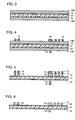
- FIGS. 3 to 6 are partial cross sections showing the steps of manufacturing the antenna coil for an IC card in accordance with the present invention.
- Figs. 3 to 6 are partial cross sections viewed from the direction along the line II-II of Fig. 1.
- an adhesive layer 12 is formed on each surface of resin film base material 11, and by the adhesive layer 12, aluminum foil 130 is fixed on each surface of resin film base material 11. In this manner, a stacked body of aluminum foils 130 and resin film base material 11 is prepared.
- a resist ink layer 14 is printed on the surface of aluminum foil 130 so as to have a prescribed eddy pattern in accordance with the specification of the antenna coil. After printing, the process for curing resist ink layer 14 is performed.
- resist ink layer 14 is removed.
- circuit pattern layer 13 is formed by using a metal plate having recesses and protrusions and a metal protrusion, whereby a contact portion or a pressure contact portion 13a of the circuit pattern layer is formed, as shown in Fig. 2.
- antenna coil 1 for an IC card in accordance with the present invention is completed.
- the resist ink used in the method of manufacturing in accordance with the present invention is not specifically limited.
- an ultraviolet curing resist ink mainly consisting of an alkali soluble resin and an acryl monomer having at least one carboxyl group in the molecule is used.
- the resist ink allows for gravure printing, has acid resistance and it can be removed easily by an alkali. Therefore, the resist ink is suitable for continuous mass production.
- the circuit pattern layer By performing gravure printing in a prescribed circuit pattern on an aluminum foil using the resist ink, curing the pattern by irradiating with ultraviolet ray, and removing the resist ink layer through a common method such as acid etching of the aluminum foil using ferric chloride and removal of the resist ink by an alkali such as sodium hydroxide, the circuit pattern layer can be formed.
- An acryl monomer having at least one carboxyl group includes, for example, 2-acryloyloxyethyl phthalic acid, 2-acryloyloxyethyl succinic acid, (2-acryloyloxyethyl) hexahydro phthalic acid, 2-acryloyloxypropyl phthalic acid, (2-acryloyloxypropyl) tetrahydro phthalic acid and (2-acryloyloxypropyl) hexahydro phthalic acid. Of these, a single acryl monomer or a mixture of two or more acryl monomers may be used.
- the aforementioned alkali soluble resin includes styrene-maleic acid copolymer resin, styrene-acrylic acid copolymer resin, and rosin-maleic acid copolymer resin.
- a common monofunctional acrylic monomer, a multifunctional acrylic monomer or a prepolymer may be added to an extent that does not hinder alkali removability, and it can prepared by appropriately adding a photopolymerization initiator, a pigment, an additive, a solvent or the like.
- the photopolymerization initiator includes benzophenone and derivative thereof, benzyl, benzoin and alkylether thereof, thioxantone and derivative thereof, RUSIRIN TPO, IRGACURE manufactured by Ciba Speciality Chemicals Inc., ESACURE manufactured by FRATTERI RAMBERTY? may be used.
- a color pigment may be added to provide visibility of the pattern, or an extender pigment such as silica, talc, clay, barium sulfate, calcium carbonate or the like may be additionally used.
- silica has an effect of preventing blocking, when the aluminum foil is to be rolled with the ultraviolet ray curing resist ink remaining thereon.
- polymerization inhibiter such as 2-tertiary butyl hydroquinone, silicon, fluorine compound, antifoaming agent such as acryl polymer, and a levelling agent are included, which may be appropriately added as needed.
- the solvent includes ethyl acetate, ethanol, denatured alcohol, isopropyl alcohol, toluene, MEK and the like, of which one may be used, or two or more of these may be used mixed with each other. It is preferred that the solvent is evaporated away from the resist ink layer by hot air drying or the like, after gravure printing.
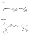
- the crimping process refers to a process for establishing physical contact between portions of aluminum foils constituting the circuit pattern layer, by destroying the resin film as the base material and the adhesive layer by means of a drill, a file, ultrasonic wave or the like: More specifically, the stacked body of the resin film and the aluminum foil are brought into contact with a metal plate having recesses and protrusions, and the stacked body is pressed by a metal protrusion, whereby the resin film as the base material and the adhesive layer are partially destroyed, allowing contact between the surfaces of the aluminum foils, establishing electrical conduction.
- Figs. 7 and 8 are enlarged photographs of a partial cross section of the stacked body including the resin film and the aluminum foils that has been subjected to the actual crimping process.
- Fig. 7 is a photomicrograph with the magnification of 48
- Fig. 8 is a photomicrograph having the magnification of 160.
- Figs. 9 and 10 are schematic illustrations of the cross sectional structures corresponding to the photographs of Figs. 7 and 8.
- a covering layer such as a white PET may be stacked by hot melt coating, for example, on the surface of the stacked body of aluminum foil and the resin film.
- the covering layer is not limited to white, and a well known color pigment, an extender pigment, metallic pigment such as aluminum flake, a known resin, varnish, vehicle or the like may be used.
- a component employed in a known IC card such as a printed layer, a magnetic recording layer, a magnetic intercepting layer, an overcoating layer, a vapor deposited layer or the like may be laminated as needed.
- Fig. 11 is a partial cross section taken along the direction of the line II-II of Fig. 1, showing an antenna coil for an IC card in accordance with another embodiment of the present invention.
- antenna coil 1 for an IC card includes a resin film base material 11, adhesive layers 12 formed on both surfaces of resin film base material 11, primer coat layers 15 as underlying coating layers formed on the surfaces of adhesive layers 12, and circuit pattern layers 13 formed of aluminum foils, formed in accordance with a prescribed pattern on the surfaces of primer coat layers 15.
- Circuit pattern layer 13 is formed in an eddy pattern on the surface of the base material as shown in Fig. 1. At an end portion of circuit pattern layer 13, areas 13c and 13d are formed, on which IC chips are mounted.
- the circuit pattern layer represented by the dotted line in Fig. 1 is positioned on the rear surface of base material 11.
- the circuit pattern layer 13 formed on the surface of base material 11 is in contact with the circuit pattern layer 13 formed on the rear surface of base material 11 to be electrically conductive at pressure contact portions 13a and 13b, respectively.
- the contact is attained by partially destroying the base material 11, adhesive layers 12 and primer coat layers 15 by the crimping process.
- the primer coat layer As the material of the primer coat layer, at least one selected from epoxy based primer, an acrylic primer, a vinyl chloride-vinyl acetate copolymer based primer and the like may be used.
- the primer coat layer has the thickness of at least 0.1 ⁇ m and at most 5.0 ⁇ m.
- the thickness of the primer coat layer is smaller than 0.1 ⁇ m, blocking tends to occur.
- the thickness of the primer coat layer exceeds 5 ⁇ m, the antenna coil comes to have large electric resistance, making conduction with other components or lines insufficient, possibly causing heat build up or malfunction.
- FIGS. 12 to 16 are partial cross sectional views showing the steps of manufacturing the antenna coil for an IC card in accordance with this another embodiment of the present invention.
- Figs. 12 to 16 are cross sections taken along the direction of the line II-II of Fig. 1.
- a primer coat layer 15 is formed on one surface of each of the two aluminum foils 130.
- primer coat process is performed at least partially and preferably on one surface of aluminum foil 130, to form a primer coat layer.
- the method of forming the primer coat layer is not particularly limited and it can be formed by brush coating, dipping, roller coater, bar coater, doctor blade, spray coating, printing or the like. Preferable method is gravure printing.
- drying and curing process is performed at a temperature of about 50 °C to about 250°C for about 5 to about 300 seconds, for sufficient curing.
- adhesive layers 12 are formed on opposing surfaces of resin film base material 11, and by the adhesive layers 12, one surface of respective ones of the aluminum foils 130 on which primer coat layer 15 has been formed is fixed on each surface of resin film base material 11. In this manner, a stacked body of aluminum foils 130 and resin film base material 11 is prepared.
- resist ink layer 14 is printed on the surface of each aluminum foil 130 to have prescribed eddy patterns in accordance with the specification of the antenna coil. After printing, curing process of the resist ink layer 14 is performed.
- circuit pattern layers 13 are formed.
- resist ink layers 14 are removed.
- a print pattern such as shown in Fig. 1 was printed using a resist ink of the following composition by helioklisho gravure printing.
- the resulting body was irradiated with an ultraviolet ray lamp having the exposure of 480 W/cm for 15 seconds to cure the resist ink, and thus a resist ink layer was formed.
- Ink composition was as follows.
- Beckacite J-896 (Rogin-maleic acid resin manufactured by Dainippon Ink & Chemicals): 21 parts by weight
- Unidic V-5510 (a mixture of prepolymer and monomer manufactured by Dainippon Ink & Chemicals): 8 parts by weight IRGACURE 184 3 parts by weight Ethyl acetate 28 parts by weight Denatured alcohol 12 parts by weight Phthalocyanine blue 1 parts by weight Silica 2 parts by weight.
- the stacked body with the resist ink layer formed in the above described manner was dipped in a hydrochloric acid solution, which was diluted at a volume ratio of 1 (hydrochloric acid) : 3 (pure water), under the etching conditions (temperature, time) as shown in Table 4, so as to etch the aluminum foil, and the circuit pattern layer in accordance with the prescribed pattern was formed. Thereafter, the stacked body was dipped in a sodium hydroxide solution of 1% at 20°C for 10 seconds, so as to remove the resist ink. Thereafter, the stacked body was dried with hot air of 70°C, whereby a stacked body such as shown in Fig. 6 was fabricated.
- an antenna coil for an IC card such as shown in Fig. 2 was fabricated.
- Table 4 represent line widths of aluminum of respective samples obtained under respective etching conditions.
- sample name etching condition aluminum line width (mm) temp. (°C) time (sec.)
- a 45 52 0.45 B 45 52 partially left C 45 52 almost fully left D 45 52 fully left
- Figs. 17-20 are photographs with the magnification of about 35 of surfaces of samples A and C etched at a temperature of 35°C for 124 seconds and samples A and C etched at a temperature of 45°C for 52 seconds, respectively.
- the linear circuit pattern layers look rough with black-white mixed pattern and the resin film base material exposed by etching aluminum foil looks gray.
- the surface of aluminum foil after the resist ink layer was removed looks black with white dots and the surface of aluminum foil left without being etched looks gray.
- Ink composition was as follows.
- Beckacite J-896 (Rogin-maleic acid resin manufactured by Dainippon Ink & Chemicals): 21 parts by weight
- Unidic V-5510 (a mixture of prepolymer and monomer manufactured by Dainippon Ink & Chemicals): 8 parts by weight IRGACURE 184 3 parts by weight Ethyl acetate 28 parts by weight Denatured alcohol 12 parts by weight Phthalocyanine blue 1 parts by weight Silica 2 parts by weight.
- the stacked body having the resist ink layer formed in the above described manner was dipped in a ferric chloride solution of 35% at 40°C for 5 minutes to etch the aluminum foil, and a circuit pattern layer in accordance with a prescribed pattern was formed. Thereafter, the stacked body was dipped in a sodium hydroxide solution of 1% at 20°C for 10 seconds, so as to remove the resist ink layer. The stacked body was dried with hot air of 70°C, whereby a stacked body such as shown in Fig. 6 was fabricated.
- an antenna coil for an IC card such as shown in Fig. 2 was fabricated.
- Antenna coils of the thus obtained samples were held in a thermostat of 150°C for 30 minutes, taken out therefrom and cooled to the room temperature. Thereafter, appearances of the antenna coils were visually observed, and thermal contraction coefficient was measured by measuring the length of the base materials, to evaluate dimensional accuracy. Results of evaluation are as shown in Table 5.
- the antenna coils of Sample Nos. 1 and 2 in accordance with the present invention had small thermal contraction coefficient and good appearance.
- the thermal contraction coefficient was small in the TD (traverse direction: direction vertical to the direction of rolling), while it was high in MD (machine direction: rolling direction), and it was recognized that dimensional accuracy of the circuit pattern layer was degraded.
- cast propylene was used as the base material, and hence it melted when held at 150°C for 30 minutes.
- polyimide film was used as the base material
- polyurethane adhesive (PU) not containing epoxy resin was used as the adhesive
- copper foil was used as the material for the circuit pattern layer. Warp was generated while it was left at the room temperature, and appearance was not satisfactory.
- epoxy coating agent No. 8800 manufactured by Tanaka Chemical Kabushiki Kaisha was applied to have the thickness of 1.5 ⁇ m after drying as the primer coat processing, on one surface of each of aluminum coils (tape-shaped) (JIS IN30-O) having the thickness of 30 ⁇ m and 20 ⁇ m, respectively, as metal foils 130, and thereafter dried and cured at a temperature of 200°C for 30 seconds. In this manner, primer coat layer 15 was formed on one surface of each of the two aluminum foil coils.
- one surface of the aluminum foil coil having the thickness of 30 ⁇ m on which primer coat layer 15 had been formed was adhered by an adhesive layer 12 to one surface of a PET film having the thickness of 38 ⁇ m as a resin film base material 11, and one surface of the aluminum foil coil having the thickness of 20 ⁇ m on which primer coat layer 15 had been formed was adhered to the other surface of the PET film, whereby a stacked body coil material was fabricated.
- An epoxy-urethane dry laminate adhesive AD76P1 manufactured by Toyo-Morton, Ltd. was used as the adhesive, and the amount of adhesive applied was 4g/m 2 by weight after drying.
- resist ink layer 14 having such a circuit pattern as shown in Fig. 1 was printed continuously and repeatedly.
- the resist ink the material similar to that used in Example 2 was used, and the amount of applied resist ink was 5 g/m 2 by weight after drying.
- resist ink layer 14 formed in this manner as a mask, the aluminum foil was etched to form a circuit pattern layer 13 as shown in Fig. 15. Ferric chloride solution was used as the etchant.
- resist ink layer 14 was removed by using sodium hydroxide solution.
- crimping process for establishing electrical conduction between the front end and back was performed using a metal plate having recesses and protrusions and a metal protrusion, at a prescribed position on the surfaces of the stacked body coil material, whereby a tape-shaped material for the antenna coils for IC cards having such a cross section as shown in Fig. 11 was fabricated.
- the tape-shaped material of the antenna coils for IC cards was rolled to a coil with a tension of 1.96 ⁇ 10 2 N/m (width) by a take up apparatus.
- the tape-shaped material of antenna coils for IC cards was fabricated through the same process steps as Example 3, except that an epoxy-melamine coating agent No. 952-H (Manufactured by Tanaka Chemical Kabushiki Kaisha) was applied to the thickness of 2 ⁇ m after drying, as the primer coat process.
- an epoxy-melamine coating agent No. 952-H Manufactured by Tanaka Chemical Kabushiki Kaisha
- the tape-shaped material of antenna coils for IC cards was fabricated through the same process steps as Example 3, except that a PEN film having the thickness of 38 ⁇ m was used as the resin film base material.
- the tape-shaped material of antenna coils for IC cards was fabricated through the same process steps as Example 3, except that an epoxy coating agent No. 8800 (manufactured by Tanaka Chemical Kabushiki Kaisha) was applied to have the thickness of 0.05 ⁇ m after drying as the primer coat process.
- an epoxy coating agent No. 8800 manufactured by Tanaka Chemical Kabushiki Kaisha
- the tape-shaped material of antenna coils for IC cards was fabricated through the same process steps as Example 3, except that an epoxy coating agent No. 8800 (manufactured by Tanaka Chemical Kabushiki Kaisha) was applied to have the thickness of 6 ⁇ m after drying as the primer coat process.
- an epoxy coating agent No. 8800 manufactured by Tanaka Chemical Kabushiki Kaisha
- a tape-shaped material of antenna coils for IC cards was fabricated through the same process steps as Example 3, except that the primer coat process was not performed on the aluminum foil coil material.
- Evaluation 5 overlapping portions are separated smooth without the necessity of pulling, when the tape-shaped material is unrolled.
- Evaluation 3 overlapping portions were separated only when a force is applied to unroll the tape-shaped material, though the force is not very strong.
- Evaluation 1 overlap portions were tightly adhered and not separated even when force was applied to unroll the tape-shaped material.
- evaluation 5 is the highest for the product of the tape-shaped material for antenna coils. In order to prevent any trouble in the subsequent manufacturing line for IC cards, the product must have the evaluation of 4 or higher.
- electrical resistance value of the crimping portions of the prepared tape-shaped materials were measured by a tester.
- the evaluation was performed by visually observing defective etching including disconnection, thinning and peeling of the circuit pattern layers. Products without any defective etching was evaluated as "good”, and products that may possibly have problems in performance as an antenna coil product was evaluated as "not good.”
- Examples 3 to 7 have the blocking evaluation of 4 or higher, while blocking evaluation is 1 for the Reference Example 1 that does not have the primer coat processing.
- Example 6 as the thickness of the primer coat layer was smaller than 0.1 ⁇ m, blocking is more likely as compared with Examples 3 to 5, so that blocking evaluation is slightly lower.
- Example 7 as the primer coat layer has the thickness larger than 5 ⁇ m, electrical resistance value of the crimping portion was increased.
Landscapes
- Engineering & Computer Science (AREA)
- Microelectronics & Electronic Packaging (AREA)
- Computer Hardware Design (AREA)
- Physics & Mathematics (AREA)
- General Physics & Mathematics (AREA)
- Theoretical Computer Science (AREA)
- Computer Networks & Wireless Communication (AREA)
- Manufacturing & Machinery (AREA)
- Credit Cards Or The Like (AREA)
Claims (12)
- Bobine d'antenne (1) pour carte à puce, comprenant :caractérisée en ce queun matériau de base (11) contenant une résine et ayant une épaisseur d'au moins 15 µm et d'au plus 70 µm ; etune couche de motif de circuit (13) formée sur une surface dudit matériau de base (11), ayant une épaisseur d'au moins 7 µm et d'au plus 60 µm, formée d'une feuille (130) contenant de l'aluminium d'au moins 97,5 % en masse et d'au plus 99,7 % en masse, etune couche adhésive (12) prise en sandwich entre ladite couche de motif de circuit (13) et ledit matériau de base (11) pour lier ladite couche de motif de circuit et ledit matériau,
la résine du matériau de base (11) a un coefficient de contraction thermique d'au plus 0,3 % après le maintien de la bobine d'antenne à 150 °C pendant 30 minutes. - Bobine d'antenne (1) pour carte à puce selon la revendication 1, dans laquelle la résine du matériau de base (11) a un coefficient de contraction thermique d'au plus 0,3 % dans chacune d'une direction usinée et d'une direction transversale.
- Bobine d'antenne (1) pour carte à puce selon la revendication 1, dans laquelle ladite feuille contient du fer pour au moins 0,7 % en masse et au plus 1,8 % en masse.
- Bobine d'antenne (1) pour carte à puce selon la revendication 1, dans laquelle ladite feuille contient du silicium pour au moins 0,03 % en masse et au plus 0,5 % en masse.
- Bobine d'antenne (1) pour carte à puce selon la revendication 1, dans laquelle ladite feuille contient du silicium pour au moins 0,03 % en masse et au plus 0,5 % en masse et du cuivre pour au moins 0,3 % en masse.
- Bobine d'antenne (1) pour carte à puce selon la revendication 1, dans laquelle ladite résine est au moins une sélectionnée à partir du groupe comprenant le polyéthylène-téréphtalate à stabilité importante des dimensions et le polyéthylène-naphtalate à stabilité importante des dimensions.
- Bobine d'antenne (1) pour carte à puce selon la revendication 1, dans laquelle ladite couche de motif de circuit (13) comprend une première couche de motif de circuit formée sur une surface dudit matériau de base (11) et une deuxième couche de motif de circuit formée sur l'autre surface dudit matériau de base (11).
- Bobine d'antenne (1) pour carte à puce selon la revendication 7, dans laquelle au moins une partie de ladite première couche de motif de circuit est en contact avec au moins une partie de ladite deuxième couche de motif de circuit pénétrant à travers ledit matériau de base (11).
- Bobine d'antenne (1) pour carte à puce selon la revendication 1, dans laquelle ladite couche adhésive (12) comprend une colle à base de polyuréthane contenant une résine époxy.
- Bobine d'antenne (1) pour carte à puce selon la revendication 1, comprenant en outre une couche de revêtement sous-jacente (15) prise en sandwich entre ladite première couche de motif de circuit (13) et ladite couche adhésive (12).
- Procédé de fabrication d'une bobine d'antenne (1) pour carte à puce selon la revendication 1, comprenant les étapes consistant à :caractérisé en ce quefixer, sur une surface d'un matériau de base (11) contenant une résine et ayant une épaisseur d'au moins 15 µm et d'au plus 70 µm, une feuille (130) contenant de l'aluminium pour au moins 97,5 % en masse et au plus 99,7 % en masse et ayant une épaisseur d'au moins 7 µm et d'au plus 60 µm en utilisant une colle (12) ;ladite étape de fixation de ladite feuille (130) comprend la fixation de ladite feuille sur une surface et sur l'autre surface dudit matériau de base (11) ; etimprimer une couche d'encre de réserve (14) ayant un motif prédéterminé sur ladite feuille (130) et graver ladite feuille (130) en utilisant ladite couche d'encre de réserve (14) comme un masque pour former une couche de motif de circuit (13) contenant de l'aluminium ; ladite couche de motif de circuit (13) comprend une première couche de motif de circuit formée sur une surface dudit matériau de base (11) et une deuxième couche de motif de circuit formée sur l'autre surface dudit matériau de base ; etaprès gravure de ladite feuille (130), enlever ladite couche d'encre de réserve (14), etamener au moins une partie de ladite première couche de motif de circuit (13) en contact avec au moins une partie de ladite deuxième couche de motif de circuit (13) par un processus de sertissage
la résine du matériau de base (11) a un coefficient de contraction thermique d'au plus 0,3 % après le maintien de la bobine d'antenne à 150 °C pendant 30 minutes. - Procédé de fabrication d'une bobine d'antenne (1) pour carte à puce selon la revendication 11, dans lequel ladite étape de fixation de ladite feuille (130) sur une surface dudit matériau de base (11) comprend la fixation de ladite feuille (130) sur une surface dudit matériau de base (11) en utilisant une colle à base de polyuréthane (12) contenant une résine époxy.
Priority Applications (1)
| Application Number | Priority Date | Filing Date | Title |
|---|---|---|---|
| EP04019210A EP1477928B1 (fr) | 2000-06-23 | 2001-06-21 | Bobine d'antenne pour carte à puce et méthode de fabrication |
Applications Claiming Priority (4)
| Application Number | Priority Date | Filing Date | Title |
|---|---|---|---|
| JP2000188592A JP2002007990A (ja) | 2000-06-23 | 2000-06-23 | Icカード用アンテナコイルとその製造方法 |
| JP2000188592 | 2000-06-23 | ||
| JP2000354383A JP2002157564A (ja) | 2000-11-21 | 2000-11-21 | Icカード用アンテナコイルとその製造方法 |
| JP2000354383 | 2000-11-21 |
Related Child Applications (1)
| Application Number | Title | Priority Date | Filing Date |
|---|---|---|---|
| EP04019210A Division EP1477928B1 (fr) | 2000-06-23 | 2001-06-21 | Bobine d'antenne pour carte à puce et méthode de fabrication |
Publications (2)
| Publication Number | Publication Date |
|---|---|
| EP1172760A1 EP1172760A1 (fr) | 2002-01-16 |
| EP1172760B1 true EP1172760B1 (fr) | 2004-12-01 |
Family
ID=26594503
Family Applications (2)
| Application Number | Title | Priority Date | Filing Date |
|---|---|---|---|
| EP01115099A Expired - Lifetime EP1172760B1 (fr) | 2000-06-23 | 2001-06-21 | Bobine d'antenne pour carte à puce et méthode de fabrication |
| EP04019210A Expired - Lifetime EP1477928B1 (fr) | 2000-06-23 | 2001-06-21 | Bobine d'antenne pour carte à puce et méthode de fabrication |
Family Applications After (1)
| Application Number | Title | Priority Date | Filing Date |
|---|---|---|---|
| EP04019210A Expired - Lifetime EP1477928B1 (fr) | 2000-06-23 | 2001-06-21 | Bobine d'antenne pour carte à puce et méthode de fabrication |
Country Status (3)
| Country | Link |
|---|---|
| US (1) | US6400323B2 (fr) |
| EP (2) | EP1172760B1 (fr) |
| DE (2) | DE60107500T2 (fr) |
Families Citing this family (114)
| Publication number | Priority date | Publication date | Assignee | Title |
|---|---|---|---|---|
| US7268740B2 (en) * | 2000-03-13 | 2007-09-11 | Rcd Technology Inc. | Method for forming radio frequency antenna |
| US7298331B2 (en) * | 2000-03-13 | 2007-11-20 | Rcd Technology, Inc. | Method for forming radio frequency antenna |
| US6476775B1 (en) * | 2000-03-13 | 2002-11-05 | Rcd Technology Corporation | Method for forming radio frequency antenna |
| JP4220252B2 (ja) * | 2001-05-17 | 2009-02-04 | エヌエックスピー ビー ヴィ | 圧着接続部によって互いに接続される製造物サブパーツを有する製造物 |
| US6693541B2 (en) * | 2001-07-19 | 2004-02-17 | 3M Innovative Properties Co | RFID tag with bridge circuit assembly and methods of use |
| JP2003108961A (ja) | 2001-09-28 | 2003-04-11 | Hitachi Ltd | 電子タグおよびその製造方法 |
| US7521271B2 (en) * | 2002-02-19 | 2009-04-21 | Nxp B.V. | Method of manufacturing a transponder |
| US6644550B1 (en) * | 2002-07-03 | 2003-11-11 | Hon Hai Precision Ind. Co., Ltd. | Electrical card connector having blocking means |
| US7456752B2 (en) * | 2003-05-06 | 2008-11-25 | Rcd Technology, Inc. | Radio frequency identification sensor for fluid level |
| US7336243B2 (en) * | 2003-05-29 | 2008-02-26 | Sky Cross, Inc. | Radio frequency identification tag |
| JP4160518B2 (ja) * | 2004-02-06 | 2008-10-01 | Dowaホールディングス株式会社 | 金属−セラミックス接合部材およびその製造方法 |
| TW200530933A (en) * | 2004-03-12 | 2005-09-16 | Renesas Tech Corp | Production process of inlet for electronic tag |
| US20060205113A1 (en) * | 2005-03-14 | 2006-09-14 | Rcd Technology Corp. | Radio frequency identification (RFID) tag lamination process |
| US7456506B2 (en) * | 2005-03-14 | 2008-11-25 | Rcd Technology Inc. | Radio frequency identification (RFID) tag lamination process using liner |
| JP4439456B2 (ja) * | 2005-03-24 | 2010-03-24 | 株式会社東芝 | 電池パック及び自動車 |
| US7315248B2 (en) * | 2005-05-13 | 2008-01-01 | 3M Innovative Properties Company | Radio frequency identification tags for use on metal or other conductive objects |
| US7891801B2 (en) * | 2005-05-30 | 2011-02-22 | Konica Minolta Medical & Graphic, Inc. | Ultraviolet ray curable ink-jet ink, ink-jet recording method and ink-jet recording apparatus |
| WO2007055433A1 (fr) * | 2005-11-10 | 2007-05-18 | Eung-Soon Chang | Procédé de fabrication d’intenne et intenne fabriquée selon le procédé |
| US7388542B2 (en) * | 2005-11-10 | 2008-06-17 | Rcd Technology, Inc. | Method for an element using two resist layers |
| US7377447B2 (en) * | 2005-12-05 | 2008-05-27 | Rcd Technology, Inc. | Tuned radio frequency identification (RFID) circuit used as a security device for wristbands and package security |
| US7519328B2 (en) * | 2006-01-19 | 2009-04-14 | Murata Manufacturing Co., Ltd. | Wireless IC device and component for wireless IC device |
| US8786510B2 (en) * | 2006-01-24 | 2014-07-22 | Avery Dennison Corporation | Radio frequency (RF) antenna containing element and methods of making the same |
| JP4557920B2 (ja) * | 2006-03-30 | 2010-10-06 | 株式会社東芝 | 非水電解質電池 |
| US9064198B2 (en) | 2006-04-26 | 2015-06-23 | Murata Manufacturing Co., Ltd. | Electromagnetic-coupling-module-attached article |
| JP4656235B2 (ja) * | 2006-04-28 | 2011-03-23 | パナソニック株式会社 | アンテナ内蔵電子回路モジュールの製造方法 |
| US20080129455A1 (en) * | 2006-05-24 | 2008-06-05 | Rcd Technology Inc. | Method for forming rfid tags |
| CN101467209B (zh) | 2006-06-30 | 2012-03-21 | 株式会社村田制作所 | 光盘 |
| DE112007002024B4 (de) | 2006-09-26 | 2010-06-10 | Murata Mfg. Co., Ltd., Nagaokakyo-shi | Induktiv gekoppeltes Modul und Element mit induktiv gekoppeltem Modul |
| CN101197462B (zh) * | 2006-12-07 | 2011-05-25 | 上海英内电子标签有限公司 | Rfid蚀刻铝天线的制造方法 |
| JP4697332B2 (ja) * | 2007-04-09 | 2011-06-08 | 株式会社村田製作所 | 無線icデバイス |
| US8235299B2 (en) | 2007-07-04 | 2012-08-07 | Murata Manufacturing Co., Ltd. | Wireless IC device and component for wireless IC device |
| EP2138962B1 (fr) | 2007-04-26 | 2012-01-04 | Murata Manufacturing Co. Ltd. | Dispositif à circuit intégré sans fil |
| EP2148449B1 (fr) | 2007-05-11 | 2012-12-12 | Murata Manufacturing Co., Ltd. | Dispositif ic sans fil |
| WO2009008296A1 (fr) | 2007-07-09 | 2009-01-15 | Murata Manufacturing Co., Ltd. | Dispositif à circuit intégré sans fil |
| JP4873079B2 (ja) | 2007-07-17 | 2012-02-08 | 株式会社村田製作所 | 無線icデバイス及び電子機器 |
| CN102915462B (zh) * | 2007-07-18 | 2017-03-01 | 株式会社村田制作所 | 无线ic器件 |
| US20090021352A1 (en) * | 2007-07-18 | 2009-01-22 | Murata Manufacturing Co., Ltd. | Radio frequency ic device and electronic apparatus |
| EP2169594B1 (fr) | 2007-07-18 | 2018-03-07 | Murata Manufacturing Co., Ltd. | Dispositif à circuit intégré sans fil et son procédé de fabrication |
| CN101578736B (zh) * | 2007-07-18 | 2013-02-27 | 株式会社村田制作所 | 无线ic器件 |
| WO2009078810A1 (fr) * | 2007-12-19 | 2009-06-25 | Linda Seah | Inlays sans contact et à interface double et procédé de fabrication de ceux-ci |
| JP4462388B2 (ja) | 2007-12-20 | 2010-05-12 | 株式会社村田製作所 | 無線icデバイス |
| EP2207240B1 (fr) | 2007-12-26 | 2013-08-21 | Murata Manufacturing Co., Ltd. | Appareil d'antenne et dispositif ci sans fil |
| EP2251933A4 (fr) * | 2008-03-03 | 2012-09-12 | Murata Manufacturing Co | Antenne composite |
| WO2009110381A1 (fr) * | 2008-03-03 | 2009-09-11 | 株式会社村田製作所 | Dispositif à ci sans fil et système de communication sans fil |
| WO2009119548A1 (fr) * | 2008-03-26 | 2009-10-01 | 株式会社村田製作所 | Dispositif radio à circuit intégré |
| CN101953025A (zh) * | 2008-04-14 | 2011-01-19 | 株式会社村田制作所 | 无线ic器件、电子设备以及无线ic器件的谐振频率调整方法 |
| CN102017298B (zh) * | 2008-05-09 | 2014-03-26 | 东洋铝株式会社 | 用于ic卡/标签的天线电路构造体及ic卡 |
| CN103295056B (zh) | 2008-05-21 | 2016-12-28 | 株式会社村田制作所 | 无线ic器件 |
| WO2009142068A1 (fr) * | 2008-05-22 | 2009-11-26 | 株式会社村田製作所 | Dispositif à circuit intégré sans fil et son procédé de fabrication |
| WO2009145007A1 (fr) * | 2008-05-26 | 2009-12-03 | 株式会社村田製作所 | Système de dispositif à ci sans fil et procédé d'authentification de dispositif à ci sans fil |
| EP3509162A1 (fr) * | 2008-05-28 | 2019-07-10 | Murata Manufacturing Co., Ltd. | Dispositif ci sans fil et composant pour un dispositif ci sans fil |
| JP4557186B2 (ja) * | 2008-06-25 | 2010-10-06 | 株式会社村田製作所 | 無線icデバイスとその製造方法 |
| JP4671001B2 (ja) * | 2008-07-04 | 2011-04-13 | 株式会社村田製作所 | 無線icデバイス |
| EP2320519B1 (fr) * | 2008-08-19 | 2017-04-12 | Murata Manufacturing Co., Ltd. | Dispositif à circuit intégré sans fil et procédé de fabrication de celui-ci |
| JP5429182B2 (ja) * | 2008-10-24 | 2014-02-26 | 株式会社村田製作所 | 無線icデバイス |
| CN102197537B (zh) * | 2008-10-29 | 2014-06-18 | 株式会社村田制作所 | 无线ic器件 |
| WO2010055945A1 (fr) * | 2008-11-17 | 2010-05-20 | 株式会社村田製作所 | Antenne et circuit intégré sans-fil |
| CN103500873B (zh) | 2009-01-09 | 2016-08-31 | 株式会社村田制作所 | 无线ic器件及无线ic模块 |
| WO2010082413A1 (fr) * | 2009-01-16 | 2010-07-22 | 株式会社村田製作所 | Dispositif haute fréquence et dispositif ci sans fil |
| CN102301528B (zh) | 2009-01-30 | 2015-01-28 | 株式会社村田制作所 | 天线及无线ic器件 |
| JP5510450B2 (ja) | 2009-04-14 | 2014-06-04 | 株式会社村田製作所 | 無線icデバイス |
| CN103022661B (zh) | 2009-04-21 | 2014-12-03 | 株式会社村田制作所 | 电子设备及天线装置的谐振频率设定方法 |
| CN102449846B (zh) | 2009-06-03 | 2015-02-04 | 株式会社村田制作所 | 无线ic器件及其制造方法 |
| WO2010146944A1 (fr) | 2009-06-19 | 2010-12-23 | 株式会社村田製作所 | Dispositif sans fil à circuits intégrés et procédé de couplage d'un circuit d'alimentation électrique et de plaques rayonnantes |
| JP5182431B2 (ja) | 2009-09-28 | 2013-04-17 | 株式会社村田製作所 | 無線icデバイスおよびそれを用いた環境状態検出方法 |
| CN102577646B (zh) | 2009-09-30 | 2015-03-04 | 株式会社村田制作所 | 电路基板及其制造方法 |
| JP5304580B2 (ja) * | 2009-10-02 | 2013-10-02 | 株式会社村田製作所 | 無線icデバイス |
| JP5522177B2 (ja) | 2009-10-16 | 2014-06-18 | 株式会社村田製作所 | アンテナ及び無線icデバイス |
| WO2011052310A1 (fr) | 2009-10-27 | 2011-05-05 | 株式会社村田製作所 | Appareil d'émission/réception et lecteur d'étiquette sans fil |
| CN102549838B (zh) | 2009-11-04 | 2015-02-04 | 株式会社村田制作所 | 通信终端及信息处理系统 |
| WO2011055701A1 (fr) | 2009-11-04 | 2011-05-12 | 株式会社村田製作所 | Terminal de communication et système de traitement de l'information |
| EP2498207B1 (fr) | 2009-11-04 | 2014-12-31 | Murata Manufacturing Co., Ltd. | Étiquette à circuit radio intégré, lecteur/enregistreur, et système de traitement d'information |
| WO2011062238A1 (fr) | 2009-11-20 | 2011-05-26 | 株式会社村田製作所 | Dispositif d'antenne et terminal de communication mobile |
| WO2011077877A1 (fr) | 2009-12-24 | 2011-06-30 | 株式会社村田製作所 | Antenne et terminal portable |
| WO2011108340A1 (fr) | 2010-03-03 | 2011-09-09 | 株式会社村田製作所 | Module de communication sans fil et dispositif de communication sans fil |
| JP5403146B2 (ja) | 2010-03-03 | 2014-01-29 | 株式会社村田製作所 | 無線通信デバイス及び無線通信端末 |
| JP5477459B2 (ja) | 2010-03-12 | 2014-04-23 | 株式会社村田製作所 | 無線通信デバイス及び金属製物品 |
| JP5370581B2 (ja) | 2010-03-24 | 2013-12-18 | 株式会社村田製作所 | Rfidシステム |
| KR101008004B1 (ko) * | 2010-03-30 | 2011-01-14 | 주식회사 연안테크놀로지 | 잉크를 이용하여 안테나 패턴이 인쇄된 휴대폰용 합성수지 부품을 제조하는 방법 |
| WO2011122163A1 (fr) | 2010-03-31 | 2011-10-06 | 株式会社村田製作所 | Antenne et dispositif de communication sans fil |
| JP5299351B2 (ja) | 2010-05-14 | 2013-09-25 | 株式会社村田製作所 | 無線icデバイス |
| JP5170156B2 (ja) | 2010-05-14 | 2013-03-27 | 株式会社村田製作所 | 無線icデバイス |
| US8981936B2 (en) | 2010-06-14 | 2015-03-17 | Avery Dennison Corporation | Method of manufacturing conductive structures |
| JP5501114B2 (ja) | 2010-06-25 | 2014-05-21 | 東洋アルミニウム株式会社 | Icカード・タグ用アンテナ回路構成体とその製造方法 |
| JP5376060B2 (ja) | 2010-07-08 | 2013-12-25 | 株式会社村田製作所 | アンテナ及びrfidデバイス |
| GB2537773A (en) | 2010-07-28 | 2016-10-26 | Murata Manufacturing Co | Antenna apparatus and communication terminal instrument |
| WO2012020748A1 (fr) | 2010-08-10 | 2012-02-16 | 株式会社村田製作所 | Carte de circuit imprimé et système de communication sans fil |
| JP5234071B2 (ja) | 2010-09-03 | 2013-07-10 | 株式会社村田製作所 | Rficモジュール |
| WO2012043432A1 (fr) | 2010-09-30 | 2012-04-05 | 株式会社村田製作所 | Dispositif à circuit intégré sans fil |
| CN105226382B (zh) | 2010-10-12 | 2019-06-11 | 株式会社村田制作所 | 天线装置及终端装置 |
| CN102971909B (zh) | 2010-10-21 | 2014-10-15 | 株式会社村田制作所 | 通信终端装置 |
| JP5510560B2 (ja) | 2011-01-05 | 2014-06-04 | 株式会社村田製作所 | 無線通信デバイス |
| JP5304956B2 (ja) | 2011-01-14 | 2013-10-02 | 株式会社村田製作所 | Rfidチップパッケージ及びrfidタグ |
| JP5370616B2 (ja) | 2011-02-28 | 2013-12-18 | 株式会社村田製作所 | 無線通信デバイス |
| JP5630566B2 (ja) | 2011-03-08 | 2014-11-26 | 株式会社村田製作所 | アンテナ装置及び通信端末機器 |
| CN103081221B (zh) | 2011-04-05 | 2016-06-08 | 株式会社村田制作所 | 无线通信器件 |
| WO2012141070A1 (fr) | 2011-04-13 | 2012-10-18 | 株式会社村田製作所 | Dispositif à circuit intégré sans fil et terminal de communication sans fil |
| JP5569648B2 (ja) | 2011-05-16 | 2014-08-13 | 株式会社村田製作所 | 無線icデバイス |
| FI125720B (fi) | 2011-05-19 | 2016-01-29 | Tecnomar Oy | Rullalta rullalle -massavalmistukseen soveltuva sähköisten siltojen valmistusmenetelmä |
| WO2013008874A1 (fr) | 2011-07-14 | 2013-01-17 | 株式会社村田製作所 | Dispositif de communication sans fil |
| JP5333707B2 (ja) | 2011-07-15 | 2013-11-06 | 株式会社村田製作所 | 無線通信デバイス |
| WO2013011865A1 (fr) | 2011-07-19 | 2013-01-24 | 株式会社村田製作所 | Module d'antenne, dispositif d'antenne, étiquette rfid et dispositif terminal de communication |
| CN203553354U (zh) | 2011-09-09 | 2014-04-16 | 株式会社村田制作所 | 天线装置及无线器件 |
| JP5344108B1 (ja) | 2011-12-01 | 2013-11-20 | 株式会社村田製作所 | 無線icデバイス及びその製造方法 |
| DE102011056326B4 (de) * | 2011-12-13 | 2019-04-04 | Infineon Technologies Ag | Chipkarten-Kontaktfeld-Anordnung |
| JP2013149015A (ja) * | 2012-01-18 | 2013-08-01 | Kyodo Printing Co Ltd | Icカード用積層体、及びicカード用積層体の製造方法 |
| WO2013115019A1 (fr) | 2012-01-30 | 2013-08-08 | 株式会社村田製作所 | Dispositif à ci sans fil |
| JP5464307B2 (ja) | 2012-02-24 | 2014-04-09 | 株式会社村田製作所 | アンテナ装置および無線通信装置 |
| CN104487985B (zh) | 2012-04-13 | 2020-06-26 | 株式会社村田制作所 | Rfid标签的检查方法及检查装置 |
| EP3016031B1 (fr) | 2013-06-25 | 2019-03-06 | Toppan Printing Co., Ltd. | Carte à double circuit intégré |
| FR3012644B1 (fr) * | 2013-10-25 | 2017-03-24 | Linxens Holding | Procede de realisation d'un circuit electrique et circuit electrique realise par ce procede |
| USD762197S1 (en) * | 2014-09-12 | 2016-07-26 | Taoglas Group Holdings Limited | GPS antenna assembly |
| US10860914B1 (en) | 2019-12-31 | 2020-12-08 | Capital One Services, Llc | Contactless card and method of assembly |
| JP7651373B2 (ja) * | 2021-05-24 | 2025-03-26 | Tdk株式会社 | アンテナ装置及びこれを備えるワイヤレス電力伝送デバイス |
Family Cites Families (10)
| Publication number | Priority date | Publication date | Assignee | Title |
|---|---|---|---|---|
| BE791269R (fr) * | 1971-11-11 | 1973-03-01 | Southwire Co | Produits trefiles en alliage d'aluminium et procede pour les |
| US5695860A (en) | 1990-08-06 | 1997-12-09 | Tokai Electronics Co., Ltd. | Resonant tag and method of manufacturing the same |
| EP0704928A3 (fr) * | 1994-09-30 | 1998-08-05 | HID Corporation | Système transpondeur radiofréquence avec interrogation à résonance parallèle et réponse à résonance en série |
| US5541399A (en) * | 1994-09-30 | 1996-07-30 | Palomar Technologies Corporation | RF transponder with resonant crossover antenna coil |
| JPH10203066A (ja) * | 1997-01-28 | 1998-08-04 | Hitachi Ltd | 非接触icカード |
| EP0886232B1 (fr) * | 1997-06-20 | 2007-09-05 | Hitachi, Ltd. | Lecteur-enregistreur, système d'alimentation et système de communication |
| DE19731969A1 (de) * | 1997-07-24 | 1998-08-27 | Siemens Ag | Verfahren zum Herstellen eines elektrischen Bauteils |
| JPH11161760A (ja) * | 1997-11-26 | 1999-06-18 | Hitachi Ltd | 薄型電子回路部品及びその製造方法及びその製造装置 |
| US6154137A (en) * | 1998-06-08 | 2000-11-28 | 3M Innovative Properties Company | Identification tag with enhanced security |
| JP3411514B2 (ja) | 1998-12-25 | 2003-06-03 | 東洋アルミニウム株式会社 | エッチング用金属箔積層体及びエッチド金属箔の製造方法 |
-
2001
- 2001-06-21 EP EP01115099A patent/EP1172760B1/fr not_active Expired - Lifetime
- 2001-06-21 US US09/886,337 patent/US6400323B2/en not_active Expired - Lifetime
- 2001-06-21 DE DE60107500T patent/DE60107500T2/de not_active Expired - Lifetime
- 2001-06-21 EP EP04019210A patent/EP1477928B1/fr not_active Expired - Lifetime
- 2001-06-21 DE DE60139036T patent/DE60139036D1/de not_active Expired - Lifetime
Also Published As
| Publication number | Publication date |
|---|---|
| US20020015002A1 (en) | 2002-02-07 |
| EP1477928A1 (fr) | 2004-11-17 |
| DE60107500D1 (de) | 2005-01-05 |
| EP1477928B1 (fr) | 2009-06-17 |
| US6400323B2 (en) | 2002-06-04 |
| DE60139036D1 (de) | 2009-07-30 |
| DE60107500T2 (de) | 2005-04-07 |
| EP1172760A1 (fr) | 2002-01-16 |
Similar Documents
| Publication | Publication Date | Title |
|---|---|---|
| EP1172760B1 (fr) | Bobine d'antenne pour carte à puce et méthode de fabrication | |
| US7021550B2 (en) | Preparing method of IC card and IC card | |
| JP2002157564A (ja) | Icカード用アンテナコイルとその製造方法 | |
| US6638635B2 (en) | IC-mounted card substrate and IC-mounted personal-data certification card | |
| CA2403130C (fr) | Procede de fabrication d'une carte de transactions financieres a revetement metallique sur laquelle sont imprimes des elements graphiques, et carte ainsi obtenue | |
| JP2009520251A (ja) | 高周波識別(rfid)アンテナを含む導電パターンを作製するための方法及び材料 | |
| MXPA03009959A (es) | Proceso de extraccion selectiva de metal para peliculas holograficas y retrorreflectoras metalizadas y dispositivos de radiofrecuencia hechos con ellas. | |
| JP2004140587A (ja) | アンテナ回路構成体およびそれを備えた機能カード | |
| KR20020042671A (ko) | 동크래드 적층판의 제조방법 | |
| WO2008013420A1 (fr) | Étiquette et procédé de préparation de celle-ci | |
| JP2002007990A (ja) | Icカード用アンテナコイルとその製造方法 | |
| JP4011425B2 (ja) | Icカード用アンテナコイル構成体、その製造方法およびそれを備えたicカード | |
| JP3634774B2 (ja) | Icカード用アンテナコイル | |
| JP2004046360A (ja) | Icカード用アンテナコイル構成体、その製造方法およびそれを備えたicカード | |
| JP4412897B2 (ja) | 貼り替え防止用ラベル | |
| JP2007226736A (ja) | Icカード及びicカード製造方法 | |
| US7451540B2 (en) | Method for fabricating a printed circuit board | |
| JP2006178549A (ja) | Icカード作製方法、icカード作製装置及びicカード | |
| JP2006178566A (ja) | Icカード作製方法、icカード作製装置及びicカード | |
| JP2005182430A (ja) | Icカードの製造方法及びicカード | |
| JP5214871B2 (ja) | 非接触icカードとその製造方法 | |
| JP4612408B2 (ja) | 回路構成体 | |
| JP2004362014A (ja) | Icカード及びicカードの製造方法 | |
| JP4841149B2 (ja) | Icカードシートの製造方法、icカード | |
| JP2005332248A (ja) | Icカード製造方法及びicカード |
Legal Events
| Date | Code | Title | Description |
|---|---|---|---|
| PUAI | Public reference made under article 153(3) epc to a published international application that has entered the european phase |
Free format text: ORIGINAL CODE: 0009012 |
|
| AK | Designated contracting states |
Kind code of ref document: A1 Designated state(s): AT BE CH CY DE DK ES FI FR GB GR IE IT LI LU MC NL PT SE TR Kind code of ref document: A1 Designated state(s): BE DE ES FR GB IT |
|
| AX | Request for extension of the european patent |
Free format text: AL;LT;LV;MK;RO;SI |
|
| 17P | Request for examination filed |
Effective date: 20020423 |
|
| 17Q | First examination report despatched |
Effective date: 20020717 |
|
| AKX | Designation fees paid |
Free format text: BE DE ES FR GB IT |
|
| GRAP | Despatch of communication of intention to grant a patent |
Free format text: ORIGINAL CODE: EPIDOSNIGR1 |
|
| GRAS | Grant fee paid |
Free format text: ORIGINAL CODE: EPIDOSNIGR3 |
|
| GRAA | (expected) grant |
Free format text: ORIGINAL CODE: 0009210 |
|
| AK | Designated contracting states |
Kind code of ref document: B1 Designated state(s): BE DE ES FR GB IT |
|
| PG25 | Lapsed in a contracting state [announced via postgrant information from national office to epo] |
Ref country code: IT Free format text: LAPSE BECAUSE OF FAILURE TO SUBMIT A TRANSLATION OF THE DESCRIPTION OR TO PAY THE FEE WITHIN THE PRESCRIBED TIME-LIMIT;WARNING: LAPSES OF ITALIAN PATENTS WITH EFFECTIVE DATE BEFORE 2007 MAY HAVE OCCURRED AT ANY TIME BEFORE 2007. THE CORRECT EFFECTIVE DATE MAY BE DIFFERENT FROM THE ONE RECORDED. Effective date: 20041201 |
|
| REG | Reference to a national code |
Ref country code: GB Ref legal event code: FG4D |
|
| REG | Reference to a national code |
Ref country code: IE Ref legal event code: FG4D |
|
| REF | Corresponds to: |
Ref document number: 60107500 Country of ref document: DE Date of ref document: 20050105 Kind code of ref document: P |
|
| PG25 | Lapsed in a contracting state [announced via postgrant information from national office to epo] |
Ref country code: ES Free format text: LAPSE BECAUSE OF FAILURE TO SUBMIT A TRANSLATION OF THE DESCRIPTION OR TO PAY THE FEE WITHIN THE PRESCRIBED TIME-LIMIT Effective date: 20050312 |
|
| PG25 | Lapsed in a contracting state [announced via postgrant information from national office to epo] |
Ref country code: GB Free format text: LAPSE BECAUSE OF NON-PAYMENT OF DUE FEES Effective date: 20050621 |
|
| PLBE | No opposition filed within time limit |
Free format text: ORIGINAL CODE: 0009261 |
|
| STAA | Information on the status of an ep patent application or granted ep patent |
Free format text: STATUS: NO OPPOSITION FILED WITHIN TIME LIMIT |
|
| ET | Fr: translation filed | ||
| 26N | No opposition filed |
Effective date: 20050902 |
|
| GBPC | Gb: european patent ceased through non-payment of renewal fee |
Effective date: 20050621 |
|
| REG | Reference to a national code |
Ref country code: FR Ref legal event code: PLFP Year of fee payment: 15 |
|
| PGFP | Annual fee paid to national office [announced via postgrant information from national office to epo] |
Ref country code: DE Payment date: 20150616 Year of fee payment: 15 |
|
| PGFP | Annual fee paid to national office [announced via postgrant information from national office to epo] |
Ref country code: BE Payment date: 20150612 Year of fee payment: 15 Ref country code: FR Payment date: 20150608 Year of fee payment: 15 |
|
| PG25 | Lapsed in a contracting state [announced via postgrant information from national office to epo] |
Ref country code: BE Free format text: LAPSE BECAUSE OF NON-PAYMENT OF DUE FEES Effective date: 20160630 |
|
| REG | Reference to a national code |
Ref country code: DE Ref legal event code: R119 Ref document number: 60107500 Country of ref document: DE |
|
| REG | Reference to a national code |
Ref country code: FR Ref legal event code: ST Effective date: 20170228 |
|
| PG25 | Lapsed in a contracting state [announced via postgrant information from national office to epo] |
Ref country code: FR Free format text: LAPSE BECAUSE OF NON-PAYMENT OF DUE FEES Effective date: 20160630 Ref country code: DE Free format text: LAPSE BECAUSE OF NON-PAYMENT OF DUE FEES Effective date: 20170103 |