EP1176459B1 - Optische Schwellwert- und Vergleichsvorrichtung und -verfahren - Google Patents
Optische Schwellwert- und Vergleichsvorrichtung und -verfahren Download PDFInfo
- Publication number
- EP1176459B1 EP1176459B1 EP20010306155 EP01306155A EP1176459B1 EP 1176459 B1 EP1176459 B1 EP 1176459B1 EP 20010306155 EP20010306155 EP 20010306155 EP 01306155 A EP01306155 A EP 01306155A EP 1176459 B1 EP1176459 B1 EP 1176459B1
- Authority
- EP
- European Patent Office
- Prior art keywords
- optical
- soa
- media
- active
- active media
- Prior art date
- Legal status (The legal status is an assumption and is not a legal conclusion. Google has not performed a legal analysis and makes no representation as to the accuracy of the status listed.)
- Expired - Lifetime
Links
Images

Classifications
-
- G—PHYSICS
- G02—OPTICS
- G02F—OPTICAL DEVICES OR ARRANGEMENTS FOR THE CONTROL OF LIGHT BY MODIFICATION OF THE OPTICAL PROPERTIES OF THE MEDIA OF THE ELEMENTS INVOLVED THEREIN; NON-LINEAR OPTICS; FREQUENCY-CHANGING OF LIGHT; OPTICAL LOGIC ELEMENTS; OPTICAL ANALOGUE/DIGITAL CONVERTERS
- G02F1/00—Devices or arrangements for the control of the intensity, colour, phase, polarisation or direction of light arriving from an independent light source, e.g. switching, gating or modulating; Non-linear optics
- G02F1/35—Non-linear optics
- G02F1/353—Frequency conversion, i.e. wherein a light beam is generated with frequency components different from those of the incident light beams
- G02F1/3536—Four-wave interaction
-
- G—PHYSICS
- G02—OPTICS
- G02F—OPTICAL DEVICES OR ARRANGEMENTS FOR THE CONTROL OF LIGHT BY MODIFICATION OF THE OPTICAL PROPERTIES OF THE MEDIA OF THE ELEMENTS INVOLVED THEREIN; NON-LINEAR OPTICS; FREQUENCY-CHANGING OF LIGHT; OPTICAL LOGIC ELEMENTS; OPTICAL ANALOGUE/DIGITAL CONVERTERS
- G02F3/00—Optical logic elements; Optical bistable devices
-
- H—ELECTRICITY
- H01—ELECTRIC ELEMENTS
- H01S—DEVICES USING THE PROCESS OF LIGHT AMPLIFICATION BY STIMULATED EMISSION OF RADIATION [LASER] TO AMPLIFY OR GENERATE LIGHT; DEVICES USING STIMULATED EMISSION OF ELECTROMAGNETIC RADIATION IN WAVE RANGES OTHER THAN OPTICAL
- H01S3/00—Lasers, i.e. devices using stimulated emission of electromagnetic radiation in the infrared, visible or ultraviolet wave range
- H01S3/10—Controlling the intensity, frequency, phase, polarisation or direction of the emitted radiation, e.g. switching, gating, modulating or demodulating
- H01S3/13—Stabilisation of laser output parameters, e.g. frequency or amplitude
- H01S3/1301—Stabilisation of laser output parameters, e.g. frequency or amplitude in optical amplifiers
- H01S3/1302—Stabilisation of laser output parameters, e.g. frequency or amplitude in optical amplifiers by all-optical means, e.g. gain-clamping
-
- G—PHYSICS
- G02—OPTICS
- G02F—OPTICAL DEVICES OR ARRANGEMENTS FOR THE CONTROL OF LIGHT BY MODIFICATION OF THE OPTICAL PROPERTIES OF THE MEDIA OF THE ELEMENTS INVOLVED THEREIN; NON-LINEAR OPTICS; FREQUENCY-CHANGING OF LIGHT; OPTICAL LOGIC ELEMENTS; OPTICAL ANALOGUE/DIGITAL CONVERTERS
- G02F1/00—Devices or arrangements for the control of the intensity, colour, phase, polarisation or direction of light arriving from an independent light source, e.g. switching, gating or modulating; Non-linear optics
- G02F1/35—Non-linear optics
- G02F1/3515—All-optical modulation, gating, switching, e.g. control of a light beam by another light beam
-
- H—ELECTRICITY
- H01—ELECTRIC ELEMENTS
- H01S—DEVICES USING THE PROCESS OF LIGHT AMPLIFICATION BY STIMULATED EMISSION OF RADIATION [LASER] TO AMPLIFY OR GENERATE LIGHT; DEVICES USING STIMULATED EMISSION OF ELECTROMAGNETIC RADIATION IN WAVE RANGES OTHER THAN OPTICAL
- H01S5/00—Semiconductor lasers
- H01S5/06—Arrangements for controlling the laser output parameters, e.g. by operating on the active medium
- H01S5/0607—Arrangements for controlling the laser output parameters, e.g. by operating on the active medium by varying physical parameters other than the potential of the electrodes, e.g. by an electric or magnetic field, mechanical deformation, pressure, light, temperature
- H01S5/0608—Arrangements for controlling the laser output parameters, e.g. by operating on the active medium by varying physical parameters other than the potential of the electrodes, e.g. by an electric or magnetic field, mechanical deformation, pressure, light, temperature controlled by light, e.g. optical switch
-
- H—ELECTRICITY
- H01—ELECTRIC ELEMENTS
- H01S—DEVICES USING THE PROCESS OF LIGHT AMPLIFICATION BY STIMULATED EMISSION OF RADIATION [LASER] TO AMPLIFY OR GENERATE LIGHT; DEVICES USING STIMULATED EMISSION OF ELECTROMAGNETIC RADIATION IN WAVE RANGES OTHER THAN OPTICAL
- H01S5/00—Semiconductor lasers
- H01S5/40—Arrangement of two or more semiconductor lasers, not provided for in groups H01S5/02 - H01S5/30
- H01S5/4025—Array arrangements, e.g. constituted by discrete laser diodes or laser bar
- H01S5/4031—Edge-emitting structures
- H01S5/4068—Edge-emitting structures with lateral coupling by axially offset or by merging waveguides, e.g. Y-couplers
-
- H—ELECTRICITY
- H01—ELECTRIC ELEMENTS
- H01S—DEVICES USING THE PROCESS OF LIGHT AMPLIFICATION BY STIMULATED EMISSION OF RADIATION [LASER] TO AMPLIFY OR GENERATE LIGHT; DEVICES USING STIMULATED EMISSION OF ELECTROMAGNETIC RADIATION IN WAVE RANGES OTHER THAN OPTICAL
- H01S5/00—Semiconductor lasers
- H01S5/50—Amplifier structures not provided for in groups H01S5/02 - H01S5/30
- H01S5/5009—Amplifier structures not provided for in groups H01S5/02 - H01S5/30 the arrangement being polarisation-insensitive
- H01S5/5018—Amplifier structures not provided for in groups H01S5/02 - H01S5/30 the arrangement being polarisation-insensitive using two or more amplifiers or multiple passes through the same amplifier
-
- H—ELECTRICITY
- H01—ELECTRIC ELEMENTS
- H01S—DEVICES USING THE PROCESS OF LIGHT AMPLIFICATION BY STIMULATED EMISSION OF RADIATION [LASER] TO AMPLIFY OR GENERATE LIGHT; DEVICES USING STIMULATED EMISSION OF ELECTROMAGNETIC RADIATION IN WAVE RANGES OTHER THAN OPTICAL
- H01S5/00—Semiconductor lasers
- H01S5/50—Amplifier structures not provided for in groups H01S5/02 - H01S5/30
- H01S5/509—Wavelength converting amplifier, e.g. signal gating with a second beam using gain saturation
Definitions
- the invention relates to optical devices and methods for optical threshold determination and for performing comparison functions, as are used in signal regeneration, pattern recognition and optical computing applications.
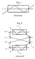
- FIG. 1 of the accompanying drawings shows an optical device as proposed by Gray et al [1].
- the proposed device is an amplifier made of an active gain medium such as a rod used for a solid state laser.
- one signal I 1 is injected straight through the gain medium and another signal I 2 is injected in a zigzag path defined by total internal reflections from the sides of the gain medium.
- the zigzag path is longer than the straight path and thus has a higher net gain. Its output is thus more sensitive to variations in the gain of the gain medium than the output from the straight path.
- This allows a signal injected in the lower gain straight path to control the gain of a signal travelling in the zigzag path by cross saturation of the gain, i.e. cross gain modulation (XGM).
- XGM cross gain modulation
- FIG. 10(a) of that reference shows another optical device proposed by Gray et al [1] (see Fig. 10(a) of that reference) which is an optical differential comparator based on two of the above-described amplifiers connected in a feedback configuration.
- a portion of the signal output from a first amplifier 1 is fed back to the control input of a second amplifier 2 by means of a partially reflecting mirror 3 and further routing components 4 which may be a sequence of waveguides or mirrors.
- the feedback action results in operation analogous to that of an electrical differential amplifier or comparator, as illustrated in Figure 10(b) of reference [1]. Threshold and logic functions are also discussed in reference [1].
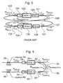
- FIG. 3 of the accompanying drawings shows a further prior art optical device according to Parolari et al [2].
- This device may be considered to be a development of the free-space device of Figure 2 proposed in reference [1].
- the device comprises two amplifier elements 120 and 130 analogous to the corresponding elements 1 and 2 of Figure 2. These are implemented as semiconductor optical amplifiers (SOA's). A portion of the output signal from the first SOA 120 is fed back to the input of the second SOA 130. Similarly, a portion of the output signal from the second SOA 130 is fed back to the input of the first SOA 120.
- Input and output side three-way couplers 123, 121, 133 and 131 are provided for this purpose, as illustrated.
- the two beams are separated spatially and thus do not interact.
- spatial separation is lost.
- spectral separation is provided by using two different wavelength ⁇ 1 and ⁇ 2 and inserting first and second optical filters 129 and 139 after their respective SOA's in order to separate the interacting signals.
- the first optical filter 129 is transmissive at the wavelength ⁇ 1 of the first SOA 120 but absorptive at the wavelength ⁇ 2 of the second SOA 130. This prevents the feedback signal P feedback ( ⁇ 2 ) being transmitted to the coupler 121 and on to the device output together with the output signal P out ( ⁇ 1 ) .
- the second optical filter 139 is transmissive at the wavelength ⁇ 2 of the second SOA 130 but absorptive at the wavelength ⁇ 1 of the first SOA 120.
- the filters 129 and 139 may be bandpass or cut-off filters. Bragg reflectors could be used, for example.
- optical isolators 124 and 134 are inserted before both SOA's. This helps suppress problems arising from the use of SOA's as the non-linear active gain medium. These SOA problems may arise from: (a) the high small signal gain for unit length; (b) parasitic oscillations which may occur due to reflections in the circuit decrease the gain available for compression; and (c) the total device efficiency. Coupling ratios are chosen from a trade off between the feedback and output powers.
- the device of Figure 3 may be considered to be a waveguide development of the free-space device of Figure 2 in which two wavelengths ⁇ 1 and ⁇ 2 are used instead of one, in conjunction with optical filters 129 and 139, and the isolators 124 and 134.
- the maximum bit rates that can be handled by the prior art devices of reference [1] and reference [2] would be limited by the carrier lifetime in the active gain medium.
- the inventors have also realised that the maximum bit rates are also limited by the propagation time associated with the feedback paths.
- the propagation time is defined by the device topology and would limit the ultimate maximum speed of any such device, if the active gain medium response time is very short.
- XGM cross phase modulation
- an optical device as defined in claim 1.
- the device and method of the first and second aspects of the invention thus fundamentally differ from those of references [1] and [2] in that the optical control signal is supplied to the active medium in the opposite direction to the optical signal to be modulated, instead of in the same direction.
- an optical memory device comprising a semiconductor laser having bistability and two injection current sources for individually controlling the bistability is known from US-A-4 748 630.
- the optical control signal is supplied in a co-propagating configuration, as in the prior art, or in the counter-propagating configuration according to the invention has little influence on the XGM effect.
- counter-propagation of the optical control signal means that separation of the optical signal and optical control signal can be obtained by the direction of propagation alone. Consequently, the optical signal and optical control signal can be the same wavelength if desired.
- there is no requirement to separate out the optical control signal from the optical signal at the output since it does not appear at the output, but rather at the input of the device, where it can be filtered out if desired by a conventional isolator, for example to suppress parasitic oscillations.
- wavelength filtering is not necessary even when the optical control signal and optical signal share the same optical path. In other words, wavelength selective filters such as band pass or band reject filters are not needed.
- the counter-propagating feedback configuration allows much shorter feedback path lengths to be achieved in comparison to what is possible with a co-propagating configuration. Consequently, much higher bit rates can be achieved, since the feedback time can be made commensurately shorter. It is estimated that the feedback path length can be made around 10 times shorter with the proposed counter-propagating configuration, than with a co-propagating configuration.
- a device according to the first aspect of the invention may be implemented with optical fibre connections and fibre couplers.
- the device may be implemented as an integrated planar waveguide device using planar waveguide connection and Y-couplers. Free-space implementation could also be achieved, but this is not envisaged to be particularly interesting for most practical applications.
- the device has fewer components and lower losses than a comparable device having a co-propagating configuration. Moreover, the device will have a lower switching power, switching power being defined as the minimum input power needed to obtain a given extinction ratio.
- the device In a planar waveguide implementation, the device will be much simpler to fabricate and bending losses can be significantly reduced, compared to a co-propagating device. In a co-propagating device, it is inevitable that the two feedback paths will need to cross, and this will add complexity to the fabrication in planar waveguide technology. By contrast, with the proposed counter-propagating feedback architecture, there is no such crossing to implement, the structure being inherently compatible with planar technology.
- the device of the first aspect of the invention can operate as a threshold circuit for determining a threshold according to the method of the second aspect of the invention. Threshold determination has many applications.
- signal regeneration can be obtained by reshaping an optical signal which enters an optical decision circuit. All signal levels below a certain decision threshold are transformed into a constant low level, and all signal levels above the decision threshold are transformed into a constant high level.
- Another application is in an all-optical pattern recognition device which needs a threshold to distinguish between auto-correlation values (when a target is recognized) and cross-correlation values (non-target sequences).
- comparison functions can also be employed in optical computing applications.
- the first and second active media are arranged so that their optical signal outputs face in the same direction.
- the first and second active media are arranged with their first and second forward directions aligned.
- the feedback path comprises a bend which is arcuate and passes through approximately 180 degrees.
- the first and second active media are arranged with their first and second forward directions opposed.
- the first and second output ports face towards each other.
- the feedback path is substantially straight, that is free of curvature liable to produce significant bending losses.
- the active media of the first and second aspects of the invention may be gain media or lossy media so that the optical signals are amplified to varying degrees or attenuated to varying degrees depending on the optical control signals.
- Figure 4 shows an optical device according to a first embodiment of the invention.
- the device comprises two amplifier elements arranged in a novel feedback configuration in which the feedback signal is fed into the amplifier in a reverse direction, which, by contrast to the prior art devices of Figures 2 and 3, has no electrical analogue.
- the device comprises first and second gain media in the form of first and second semiconductor optical amplifiers (SOA's) 20 and 30 extending along respective optical axes.
- a first port of each SOA is arranged on the input side of the SOA to receive and inject a signal to be modulated through that SOA generally in a first direction along the optical axis.
- Each input signal has a power P in and propagates in the direction indicated by the accompanying arrows in the figure.
- a second port is arranged on the output side of each SOA to receive and output the signal after it has traversed and been modulated by the gain medium to reach a power P out .
- the second port also serves to receive and inject a feedback optical control signal of power P feedback into that SOA in a second direction opposed to the first direction.
- the feedback optical control signal acts to vary the gain of the SOA experienced by the signal input from the first port.
- the first SOA (SOA 1) 20 has a first propagation path along which a first optical signal, input as signal P in1 ( ⁇ 1 ) , travels in a first forward direction.
- the second SOA (SOA 2) 30 has a second propagation path along which a second optical signal input as P in2 ( ⁇ 2 ) travels in a second forward direction.
- a feedback path 40 is provided that interconnects the outputs of the first and second SOA's 20 and 30.
- a portion of the first optical signal output from the SOA 20 is supplied backwards into the output of the second SOA 30 as a feedback optical control signal P feedback1 ( ⁇ 1 ) .
- a portion of the second optical signal P out2 ( ⁇ 2 ) output from the SOA 30 is supplied backwards into the output of the first SOA 20 as a feedback optical control signal P feedback2 ( ⁇ 2 ) .
- P feedback1 ⁇ 1
- P out2 ( ⁇ 2 ) output from the SOA 30 is supplied backwards into the output of the first SOA 20 as a feedback optical control signal P feedback2 ( ⁇ 2 ) .
- P feedback2 ⁇ 2
- the feedback signals are injected into the SOA's and travel backwards through them along the respective propagation paths in a reverse direction opposite to the forward propagation direction of the optical signals injected at the input side of the device.
- the reverse travelling feedback signals thus act as control signals for the forward travelling optical signals by virtue of the XGM effect.
- the feedback action is thus based on XGM into both SOA's as defined by the powers of the feedback signals P feedback1 and P feedback2 .
- an optical coupler (C 1 ) 22 is arranged in the feedback path 40.
- the ratio of the coupler 22 defines the power ratio P out1 ( ⁇ 1 ):P feedback1 ( ⁇ 1 ) between the signal output from the first arm of the device and the signal fed back to the second SOA 30.
- an optical coupler (C 2 ) 32 is arranged in the feedback path 40.
- the ratio of the coupler 32 defines the power ratio P out2 ( ⁇ 2 ): P feedback2 ( ⁇ 2 ) between the signal output from the second arm of the device and the signal fed back to the first SOA 20.
- the coupler 32 (or 22) could be removed, or the output P out2 ( ⁇ 2 ) (or P out1 ( ⁇ 1 ) ) not utilised.
- respective optical isolators 24 and 34 are inserted in order to filter out the feedback signals after traversal of the respective SOA's 20 and 30, thus to suppress parasitic oscillations due to back reflections.
- couplers 26 and 36 are placed before the device. These couplers were used in the prototype to monitor the input signals and are not part of the device itself.
- the device also includes a filter 42 placed in the feedback path 40, namely between C 1 and C 2 , to filter out the amplified spontaneous emission (ASE) originating from the SOA's.
- ASE amplified spontaneous emission
- the SOA's ASE power otherwise alters signal gain compression efficiency.
- the first SOA 20 is an Optospeed MRI/X -500.
- the second SOA 30 is an Alcatel M1008. Their outputs are connected by two fibre couplers, C 1 and C 2 , which couple part of the output power of each SOA into the other. The couplers are 90/10 so that 90% of the output power of the first SOA 20 at ⁇ 1 enters the second SOA 30 through coupler C 2 . Similarly, 90% of the output power of the second SOA 30 at ⁇ 2 enters the first SOA 20 through coupler C 1 . Thus, about 81% of the output power of the first SOA 20 is coupled into the second SOA 30 and vice versa to provide the feedback action.
- This choice of coupling ratio is a tradeoff between high feedback power and acceptable levels of output power, P out1 and P out2 .
- the coupling ratio of the couplers C 1 and C 2 can be chosen as desired for the application concerned.
- ⁇ 1 and ⁇ 2 could be the same wavelength which would not be possible in a co-propagating architecture.
- the counter-propagating XGM architecture of the device means that separation between signals is provided by the sense of propagation. Wavelength filtering is not needed.
- the device has two main operating points according to the relative balance between the two input powers in the SOA's. In these two equilibrium states, the device outputs are complementary, i.e. the high level of P out1 corresponds to the low level of P out2 and vice versa.
- the high level equilibrium state of P out2 ( ⁇ 2 ) is maintained as long as P in1 ( ⁇ 1 ) is sufficiently low and P out1 ( ⁇ 1 ) and P feedback1 ( ⁇ 1 ) are consequently low.
- SOA 2 gain is not compressed and P out2 ( ⁇ 2 ) is high.
- P feedback2 ( ⁇ 2 ) is greater than SOA 1 saturation power, it compresses SOA 1 gain thus keeping P feedback1 ( ⁇ 1 ) low.
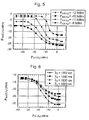
- Figure 5 shows experimental data of the response of the device of Figure 4 in terms of a graph of output power P out2 ( ⁇ 2 ) plotted versus P in1 ( ⁇ 1 ) for four different values of P in2 ( ⁇ 2 ) of -6.5 dBm, -12.5dBm, -17.5 dBm and -22.5 dBm.
- the threshold input is P in1 which is varied to test the device, while P in2 is fixed at each of four different values.
- the threshold output P out2 is measured which is high when P in1 is low, and switches to a low value when P in1 is high.
- the behaviour of the device has been further tested to compile the results shown in the table below which outlines the circuit performance in terms of output extinction ratio.
- Switching transient, switching power and extinction ratio values are conditioned by the SOA gain and P in2 .
- SOA gain is a function of operating wavelength, bias current and amplifying waveguide parameter.
- Figure 6 shows further response characteristics of the device of Figure 4.
- a series of curves show the behaviour of the device in terms of P out2 ( ⁇ 2 ) versus P in1 ( ⁇ 1 ) as one of the input wavelengths ⁇ 2 (and thus gain) is changed.
- the device of the first embodiment can operate both as a threshold circuit (when P in2 is fixed) and as a comparator (when both P in1 and P in2 vary).
- the response speed of the device is now considered.
- Two of the limiting factors for the speed of response are: (i) the inherent SOA XGM response which is well known to be less than 100 ps; and (ii) the physical propagation time of the feedback signal in the feedback path.
- the inherent SOA XGM response can thus be neglected, the response time being limited by the feedback path length.
- An integrated fibre implementation of the device of the first embodiment should allow a feedback path of only a few centimetres, where the limiting length is not attributable to the SOA's (length of the order of 1 mm) but rather the integrated coupling circuit length, specifically the length of the feedback path 40. Even shorter feedback path lengths may be possible in integrated planar waveguide implementations. In fact, still shorter path lengths are possible in the devices of the second and third embodiments discussed further below.
- a comparison between the prior art device of Figure 3 and the first embodiment device of Figure 4 is now made.
- a fundamental difference is that the device of Figure 3 uses feedback conforming to an electrical circuit analogy in which the output of one SOA is fed back to the input of the other SOA and vice versa, whereas the device of Figure 4 uses feedback that has no electrical circuit analogy in which the output of one SOA is fed into the output of the other SOA and vice versa.
- the arrangement of Figure 3 is referred to as a co-propagating configuration, because the optical signal to be modulated propagates in the same direction through the SOA as the controlling feedback signal.
- Figure 4 the arrangement of Figure 4 is referred to as a counter-propagating configuration, because the optical control signal fed into one SOA from the output of the other SOA is fed in backwards at the SOA output to propagate through the SOA in the reverse direction as compared to the optical signal to be modulated.
- Figure 7 shows an optical device according to a second embodiment of the invention.
- the second embodiment will mainly be understood from the first embodiment of Figure 4, the above description of which is referred to. In the following, the second embodiment is thus discussed in relation to its differences from the first embodiment.
- the principal difference between the first and second embodiments is the replacement of the two three-way couplers 22 and 32 with one four-way coupler 28.
- This change is elegant in that a further component is eliminated, thus further reducing losses, as well as complexity and cost.
- Figure 8 shows an optical device according to a third embodiment of the invention.
- the third embodiment may be considered to be a planar waveguide implementation of the second embodiment.
- the device is based on an integrated bidirectional coupler 28, functionally equivalent to the four-way fibre coupler 28 of the second embodiment, and fabricated on a chip 10.
- Two SOA's 20 and 30 are deposited in waveguides leading to the coupler 28, functionally equivalent to the SOA's of the second embodiment.
- the device function will be understood in all other respects with reference to the second embodiment. Additional isolators (not shown) may also be provided, as in the second embodiment.
- the two SOA's 20 and 30 are arranged facing each other with a feedback path that does not curve back on itself but.
- the arrangement of the third embodiment has the advantage that the feedback path can be made still shorter, thus further reducing the propagation time of the feedback signal.
- the feedback path length will be limited by the minimum radius of curvature for acceptable bending losses in the feedback path.
- this design limitation is removed.
- the outputs may bend to emerge from the chip parallel to the inputs, as illustrated in Figure 8, so that all input and outputs are from the ends of the chip 10.
- the outputs from the (rectangular) chip may be lateral to the inputs.
- the outputs may come from the sides of the chip with the inputs at the ends.
- Other variations are also possible.
- FIG. 9 is a schematic diagram of a fourth embodiment of the invention, which may be considered to be a modification of the first embodiment and is specifically for performing threshold functions.
- the principal difference between the first and fourth embodiments is that, in the fourth embodiment, instead of input of a separate second input signal for the second gain medium 30, the second optical control signal P feedback1 ( ⁇ 1 ) is reflected back into the second gain medium by a mirror 31. The reflected second optical control signal thus serves as the second optical signal P in2 ( ⁇ 2 ).
- An external comparison signal is thus dispensed with, the output P out1 ( ⁇ 1 ) being a function purely of the single input P in1 ( ⁇ 1 ) to provide a threshold function.
- the value of the threshold can be set passively or dynamically through choice or control of the gain medium (SOA) and the reflectivity of the mirror 31.
- the mirror 31 may be implemented as a Bragg reflector.
- a dielectric mirror could be deposited on the end of an optical fibre.
- the mirror may be deposited on the cleaved edge of the waveguide chip, or may be internal to a planar waveguide.
Landscapes
- Physics & Mathematics (AREA)
- Nonlinear Science (AREA)
- Optics & Photonics (AREA)
- General Physics & Mathematics (AREA)
- Electromagnetism (AREA)
- Engineering & Computer Science (AREA)
- Plasma & Fusion (AREA)
- Optical Integrated Circuits (AREA)
Claims (21)
- Optische Vorrichtung, welche aufweist:(a) ein erstes aktives Medium (20), das einen ersten Eingangsport und einen ersten Ausgangsport aufweist, die so angeordnet sind, dass ein erster Ausbreitungsweg zum Durchgang eines ersten optischen Signals (Pin1) in einer ersten Vorwärtsrichtung zwischen dem ersten Eingangsport und dem ersten Ausgangsport festgelegt wird;(b) ein zweites aktives Medium (30), das einen zweiten Eingangsport und einen zweiten Ausgangsport aufweist, die so angeordnet sind, dass ein zweiter Ausbreitungsweg zum Durchgang eines zweiten optischen Signals (Pin1) in einer zweiten Vorwärtsrichtung zwischen dem zweiten Eingangsport und dem zweiten Ausgangsport festgelegt wird;(c) einen Rückkopplungsweg (40), der das erste und das zweite aktive Medium verbindet, um so zumindest einen Anteil des ersten und zweiten optischen Signals von dem ersten und zweiten Ausgangsport zu dem zweiten und ersten Ausgangsport als jeweiliges zweites bzw. erstes optisches Steuersignal zu leiten, zur Ausbreitung entlang dem zweiten und ersten Ausbreitungsweg in einer zweiten und einer ersten Rückwärtsrichtung, die entgegengesetzt zur zweiten und ersten Vorwärtsrichtung verlaufen, sodass im Gebrauch das erste und das zweite optische Steuersignal die Modulation variieren, die auf das erste und das zweite optische Signal bei deren jeweiligem Durchqueren des ersten und des zweiten aktiven Mediums einwirkt.
- Vorrichtung nach Anspruch 1, bei welcher der erste und der zweite Ausgangsport in dieselbe Richtung weisen.
- Vorrichtung nach Anspruch 1 oder 2, bei welcher das erste und das zweite aktive Medium so angeordnet sind, dass ihre erste und zweite Vorwärtsrichtung ausgerichtet sind.
- Vorrichtung nach Anspruch 1, 2 oder 3, bei welcher der Rückkopplungsweg eine Biegung aufweist.
- Vorrichtung nach Anspruch 1, bei welcher das erste und das zweite aktive Medium so angeordnet sind, dass ihre erste und zweite Vorwärtsrichtung entgegengesetzt sind.
- Vorrichtung nach Anspruch 1 oder 5, bei welcher der erste und der zweite Ausgangsport zueinander hinweisen.
- Vorrichtung nach Anspruch 1, 5 oder 6, bei welcher der Rückkopplungsweg im Wesentlichen geradlinig ist.
- Vorrichtung nach einem der voranstehenden Ansprüche, bei welcher der Rückkopplungsweg ein Wellenleiter ist, der gemeinsam von dem ersten und dem zweiten optischen Steuersignal genutzt wird, die sich entlang dem Wellenleiter in entgegengesetzten Richtungen ausbreiten.
- Vorrichtung nach einem der voranstehenden Ansprüche, mit einem ersten optischen Isolator (24), der so angeordnet ist, dass er die ersten optischen Steuersignale nach dem Durchqueren des ersten aktiven Mediums in der ersten Rückwärtsrichtung herausfiltert.
- Vorrichtung nach einem der voranstehenden Ansprüche, mit einem zweiten optischen Isolator (34), der so angeordnet ist, dass er das zweite optische Steuersignale nach dem Durchqueren des zweiten aktiven Mediums in der zweiten Rückwärtsrichtung herausfiltert.
- Vorrichtung nach einem der voranstehenden Ansprüche, mit zumindest einem Mehrwege-Optikelement (22, 32), das so in dem Rückkopplungsweg angeordnet ist, dass es einen Teil zumindest entweder des ersten oder des zweiten optischen Signals von dem ersten und zweiten Ausgangsport aus dem Rückkopplungsweg zur Ausgabe von der Vorrichtung umleitet.
- Vorrichtung nach einem der Ansprüche 1 bis 11, bei welcher das erste und das zweite aktive Medium und der Rückkopplungsweg in einer ebenen Wellenleiteranordnung vereinigt sind.
- Vorrichtung nach einem der Ansprüche 1 bis 11, bei welcher das erste und das zweite aktive Medium diskrete Bauteile sind, und der Rückkopplungsweg eine Lichtleitfaser-Wellenleiteranordnung aufweist.
- Vorrichtung nach einem der Ansprüche 1 bis 13, bei welcher das erste und das zweite aktive Medium Verstärkungsmedien sind.
- Vorrichtung nach einem der Ansprüche 1 bis 13, bei welcher das erste und das zweite aktive Medium verlustbehaftete Medien sind.
- Vorrichtung nach einem der voranstehenden Ansprüche, mit einem Reflektor (31), der so angeordnet ist, dass er das zweite optische Steuersignal zurück durch das zweite aktive Medium als das zweite optische Signal reflektiert.
- Verfahren zum Modulieren eines optischen Signals, bei welchem vorgesehen sind:(a) Bereitstellung eines ersten und eines zweiten aktiven Mediums (20, 30);(b) Zuführen eines ersten und eines zweiten optischen Signals (Pin1, Pin2) zum Durchqueren des ersten und des zweiten aktiven Mediums in einer ersten und einer zweiten Vorwärtsrichtung; und(c) Umleiten zumindest eines Anteils des ersten und des zweiten optischen Signals, nach Durchquerung des ersten und des zweiten aktiven Mediums, auf das zweite und erste aktive Medium als zweites bzw. erstes optisches Steuersignal, wobei das erste und das zweite optische Steuersignal durch das erste und das zweite aktive Medium in einer ersten und einer zweiten Rückwärtsrichtung entgegengesetzt zu der ersten und der zweiten Vorwärtsrichtung zugeführt werden, sodass das erste und das zweite optische Steuersignal die Modulation variieren, die auf das erste und das zweite optische Signal bei deren jeweiligem Durchqueren des ersten und des zweiten aktiven Mediums einwirkt.
- Verfahren nach Anspruch 17, bei welchem das zweite optische Signal im Wesentlichen invariant ist, und als ein Referenzsignal dient, und das Verfahren eine Schwellenwertbestimmung zur Verfügung stellt.
- Verfahren nach Anspruch 17, bei welchem das erste und das zweite optische Signal variabel sind, und das Verfahren eine Vergleichsfunktion zur Verfügung stellt.
- Verfahren nach Anspruch 17, 18 oder 19, bei welchem das erste und das zweite aktive Medium Verstärkungsmedien sind, sodass das erste und das zweite optische Steuersignal die Verstärkung variieren, die auf das erste und das zweite optische Signal einwirkt.
- Verfahren nach Anspruch 17, 18 oder 19, bei welchem das erste und das zweite aktive Medium verlustbehaftete Medien sind, sodass das erste und das zweite optische Steuersignal die Abschwächung variieren, die auf das erste und das zweite optische Signal einwirkt.
Priority Applications (1)
| Application Number | Priority Date | Filing Date | Title |
|---|---|---|---|
| EP20010306155 EP1176459B1 (de) | 2000-07-28 | 2001-07-18 | Optische Schwellwert- und Vergleichsvorrichtung und -verfahren |
Applications Claiming Priority (3)
| Application Number | Priority Date | Filing Date | Title |
|---|---|---|---|
| EP00306465 | 2000-07-28 | ||
| EP00306465 | 2000-07-28 | ||
| EP20010306155 EP1176459B1 (de) | 2000-07-28 | 2001-07-18 | Optische Schwellwert- und Vergleichsvorrichtung und -verfahren |
Publications (2)
| Publication Number | Publication Date |
|---|---|
| EP1176459A1 EP1176459A1 (de) | 2002-01-30 |
| EP1176459B1 true EP1176459B1 (de) | 2007-03-07 |
Family
ID=26073259
Family Applications (1)
| Application Number | Title | Priority Date | Filing Date |
|---|---|---|---|
| EP20010306155 Expired - Lifetime EP1176459B1 (de) | 2000-07-28 | 2001-07-18 | Optische Schwellwert- und Vergleichsvorrichtung und -verfahren |
Country Status (1)
| Country | Link |
|---|---|
| EP (1) | EP1176459B1 (de) |
Families Citing this family (3)
| Publication number | Priority date | Publication date | Assignee | Title |
|---|---|---|---|---|
| ES2209629B1 (es) * | 2002-07-25 | 2005-04-01 | Universidad Politecnica De Valencia | Metodo y dispositivo para comparar dos secuencias de bits, en un entorno completamente optico. |
| EP2269115B1 (de) * | 2008-04-25 | 2011-12-21 | Telefonaktiebolaget L M Ericsson (PUBL) | Optisches flipflop |
| WO2017033197A1 (en) * | 2015-08-27 | 2017-03-02 | Bar-Ilan University | Multi optically-coupled channels module and related methods of computation |
Family Cites Families (3)
| Publication number | Priority date | Publication date | Assignee | Title |
|---|---|---|---|---|
| US4748630A (en) * | 1985-01-17 | 1988-05-31 | Nec Corporation | Optical memory device comprising a semiconductor laser having bistability and two injection current sources for individually controlling the bistability |
| US5537243A (en) * | 1993-12-17 | 1996-07-16 | At&T Corp. | All-optical flip-flop |
| US5999284A (en) * | 1997-06-05 | 1999-12-07 | Northern Telecom Limited | Optical detection and logic devices with latching function |
-
2001
- 2001-07-18 EP EP20010306155 patent/EP1176459B1/de not_active Expired - Lifetime
Also Published As
| Publication number | Publication date |
|---|---|
| EP1176459A1 (de) | 2002-01-30 |
Similar Documents
| Publication | Publication Date | Title |
|---|---|---|
| US6597497B2 (en) | Semiconductor optical amplifier with transverse laser cavity intersecting optical signal path and method of fabrication thereof | |
| US6577654B1 (en) | Optical signal power monitor and regulator | |
| KR100343490B1 (ko) | 전-광학플립플롭용장치 | |
| JPH08213684A (ja) | 同調可能なレーザ装置 | |
| JPH02276285A (ja) | フォトトランジスタ | |
| JPH02199430A (ja) | 半導体光スイッチ及び半導体光スイッチアレイ | |
| JPH1039264A (ja) | 増幅を伴う単一ポート変調器のための装置および方法 | |
| JP3165608B2 (ja) | 光インバータおよびこれを構成する方法 | |
| JP3044180B2 (ja) | 光周波数トランスレータ | |
| US6766072B2 (en) | Optical threshold and comparison devices and methods | |
| US7065300B1 (en) | Optical transmitter including a linear semiconductor optical amplifier | |
| US7020168B2 (en) | High power multi-frequency laser | |
| JP4022792B2 (ja) | 半導体光増幅装置 | |
| JP3989374B2 (ja) | 光制御装置 | |
| EP1176459A1 (de) | Optische Schwellwert- und Vergleichsvorrichtung und -verfahren | |
| CA2354461C (en) | Optical threshold and comparison devices and methods | |
| CA2352351C (en) | Multiwavelength light source device employing annular optical delay circuit | |
| JPH06504407A (ja) | 干渉計 | |
| US7362928B2 (en) | Optical switch and gate apparatus and method | |
| JP2836359B2 (ja) | 光ファイバ増幅器用励起光源バックアップ方法 | |
| JP2806426B2 (ja) | 光スイッチ | |
| JP3268539B2 (ja) | 偏波利用光素子 | |
| JPH10228039A (ja) | 導波型光アレスター | |
| Yeo et al. | Performance of DPSK and NRZ-OOK signals in a novel folded-path optical packet switch buffer | |
| JP2850955B2 (ja) | 光スイッチ |
Legal Events
| Date | Code | Title | Description |
|---|---|---|---|
| PUAI | Public reference made under article 153(3) epc to a published international application that has entered the european phase |
Free format text: ORIGINAL CODE: 0009012 |
|
| AK | Designated contracting states |
Kind code of ref document: A1 Designated state(s): AT BE CH CY DE DK ES FI FR GB GR IE IT LI LU MC NL PT SE TR |
|
| AX | Request for extension of the european patent |
Free format text: AL;LT;LV;MK;RO;SI |
|
| 17P | Request for examination filed |
Effective date: 20020711 |
|
| AKX | Designation fees paid |
Free format text: AT BE CH CY DE DK ES FI FR GB GR IE IT LI LU MC NL PT SE TR |
|
| RAP1 | Party data changed (applicant data changed or rights of an application transferred) |
Owner name: PIRELLI S.P.A. |
|
| RAP1 | Party data changed (applicant data changed or rights of an application transferred) |
Owner name: PIRELLI & C. S.P.A. |
|
| GRAP | Despatch of communication of intention to grant a patent |
Free format text: ORIGINAL CODE: EPIDOSNIGR1 |
|
| GRAS | Grant fee paid |
Free format text: ORIGINAL CODE: EPIDOSNIGR3 |
|
| GRAJ | Information related to disapproval of communication of intention to grant by the applicant or resumption of examination proceedings by the epo deleted |
Free format text: ORIGINAL CODE: EPIDOSDIGR1 |
|
| GRAL | Information related to payment of fee for publishing/printing deleted |
Free format text: ORIGINAL CODE: EPIDOSDIGR3 |
|
| 17Q | First examination report despatched |
Effective date: 20041222 |
|
| GRAP | Despatch of communication of intention to grant a patent |
Free format text: ORIGINAL CODE: EPIDOSNIGR1 |
|
| GRAS | Grant fee paid |
Free format text: ORIGINAL CODE: EPIDOSNIGR3 |
|
| GRAA | (expected) grant |
Free format text: ORIGINAL CODE: 0009210 |
|
| AK | Designated contracting states |
Kind code of ref document: B1 Designated state(s): AT BE CH CY DE DK ES FI FR GB GR IE IT LI LU MC NL PT SE TR |
|
| PG25 | Lapsed in a contracting state [announced via postgrant information from national office to epo] |
Ref country code: CH Free format text: LAPSE BECAUSE OF FAILURE TO SUBMIT A TRANSLATION OF THE DESCRIPTION OR TO PAY THE FEE WITHIN THE PRESCRIBED TIME-LIMIT Effective date: 20070307 Ref country code: AT Free format text: LAPSE BECAUSE OF FAILURE TO SUBMIT A TRANSLATION OF THE DESCRIPTION OR TO PAY THE FEE WITHIN THE PRESCRIBED TIME-LIMIT Effective date: 20070307 Ref country code: BE Free format text: LAPSE BECAUSE OF FAILURE TO SUBMIT A TRANSLATION OF THE DESCRIPTION OR TO PAY THE FEE WITHIN THE PRESCRIBED TIME-LIMIT Effective date: 20070307 Ref country code: NL Free format text: LAPSE BECAUSE OF FAILURE TO SUBMIT A TRANSLATION OF THE DESCRIPTION OR TO PAY THE FEE WITHIN THE PRESCRIBED TIME-LIMIT Effective date: 20070307 Ref country code: LI Free format text: LAPSE BECAUSE OF FAILURE TO SUBMIT A TRANSLATION OF THE DESCRIPTION OR TO PAY THE FEE WITHIN THE PRESCRIBED TIME-LIMIT Effective date: 20070307 Ref country code: FI Free format text: LAPSE BECAUSE OF FAILURE TO SUBMIT A TRANSLATION OF THE DESCRIPTION OR TO PAY THE FEE WITHIN THE PRESCRIBED TIME-LIMIT Effective date: 20070307 |
|
| REG | Reference to a national code |
Ref country code: GB Ref legal event code: FG4D |
|
| REG | Reference to a national code |
Ref country code: CH Ref legal event code: EP |
|
| REF | Corresponds to: |
Ref document number: 60127045 Country of ref document: DE Date of ref document: 20070419 Kind code of ref document: P |
|
| REG | Reference to a national code |
Ref country code: DE Ref legal event code: R096 Ref document number: 60127045 Country of ref document: DE Effective date: 20070419 |
|
| REG | Reference to a national code |
Ref country code: IE Ref legal event code: FG4D |
|
| PG25 | Lapsed in a contracting state [announced via postgrant information from national office to epo] |
Ref country code: SE Free format text: LAPSE BECAUSE OF FAILURE TO SUBMIT A TRANSLATION OF THE DESCRIPTION OR TO PAY THE FEE WITHIN THE PRESCRIBED TIME-LIMIT Effective date: 20070607 |
|
| PG25 | Lapsed in a contracting state [announced via postgrant information from national office to epo] |
Ref country code: ES Free format text: LAPSE BECAUSE OF FAILURE TO SUBMIT A TRANSLATION OF THE DESCRIPTION OR TO PAY THE FEE WITHIN THE PRESCRIBED TIME-LIMIT Effective date: 20070618 |
|
| PG25 | Lapsed in a contracting state [announced via postgrant information from national office to epo] |
Ref country code: PT Free format text: LAPSE BECAUSE OF FAILURE TO SUBMIT A TRANSLATION OF THE DESCRIPTION OR TO PAY THE FEE WITHIN THE PRESCRIBED TIME-LIMIT Effective date: 20070807 |
|
| NLV1 | Nl: lapsed or annulled due to failure to fulfill the requirements of art. 29p and 29m of the patents act | ||
| REG | Reference to a national code |
Ref country code: CH Ref legal event code: PL |
|
| PLBE | No opposition filed within time limit |
Free format text: ORIGINAL CODE: 0009261 |
|
| STAA | Information on the status of an ep patent application or granted ep patent |
Free format text: STATUS: NO OPPOSITION FILED WITHIN TIME LIMIT |
|
| PG25 | Lapsed in a contracting state [announced via postgrant information from national office to epo] |
Ref country code: DK Free format text: LAPSE BECAUSE OF FAILURE TO SUBMIT A TRANSLATION OF THE DESCRIPTION OR TO PAY THE FEE WITHIN THE PRESCRIBED TIME-LIMIT Effective date: 20070307 |
|
| 26N | No opposition filed |
Effective date: 20071210 |
|
| REG | Reference to a national code |
Ref country code: DE Ref legal event code: R097 Ref document number: 60127045 Country of ref document: DE Effective date: 20071210 |
|
| PG25 | Lapsed in a contracting state [announced via postgrant information from national office to epo] |
Ref country code: MC Free format text: LAPSE BECAUSE OF NON-PAYMENT OF DUE FEES Effective date: 20070731 Ref country code: GR Free format text: LAPSE BECAUSE OF FAILURE TO SUBMIT A TRANSLATION OF THE DESCRIPTION OR TO PAY THE FEE WITHIN THE PRESCRIBED TIME-LIMIT Effective date: 20070608 |
|
| PG25 | Lapsed in a contracting state [announced via postgrant information from national office to epo] |
Ref country code: IE Free format text: LAPSE BECAUSE OF NON-PAYMENT OF DUE FEES Effective date: 20070718 |
|
| PG25 | Lapsed in a contracting state [announced via postgrant information from national office to epo] |
Ref country code: CY Free format text: LAPSE BECAUSE OF FAILURE TO SUBMIT A TRANSLATION OF THE DESCRIPTION OR TO PAY THE FEE WITHIN THE PRESCRIBED TIME-LIMIT Effective date: 20070307 |
|
| PG25 | Lapsed in a contracting state [announced via postgrant information from national office to epo] |
Ref country code: LU Free format text: LAPSE BECAUSE OF NON-PAYMENT OF DUE FEES Effective date: 20070718 |
|
| PG25 | Lapsed in a contracting state [announced via postgrant information from national office to epo] |
Ref country code: TR Free format text: LAPSE BECAUSE OF FAILURE TO SUBMIT A TRANSLATION OF THE DESCRIPTION OR TO PAY THE FEE WITHIN THE PRESCRIBED TIME-LIMIT Effective date: 20070307 |
|
| REG | Reference to a national code |
Ref country code: DE Ref legal event code: R081 Ref document number: 60127045 Country of ref document: DE Owner name: GOOGLE, INC., US Free format text: FORMER OWNER: PIRELLI & C. S.P.A., MAILAND/MILANO, IT Effective date: 20120209 Ref country code: DE Ref legal event code: R082 Ref document number: 60127045 Country of ref document: DE Representative=s name: MANITZ, FINSTERWALD & PARTNER GBR, DE Effective date: 20120209 Ref country code: DE Ref legal event code: R081 Ref document number: 60127045 Country of ref document: DE Owner name: GOOGLE, INC., MOUNTAIN VIEW, US Free format text: FORMER OWNER: PIRELLI & C. S.P.A., MAILAND/MILANO, IT Effective date: 20120209 Ref country code: DE Ref legal event code: R082 Ref document number: 60127045 Country of ref document: DE Representative=s name: MANITZ FINSTERWALD PATENTANWAELTE PARTMBB, DE Effective date: 20120209 Ref country code: DE Ref legal event code: R081 Ref document number: 60127045 Country of ref document: DE Owner name: GOOGLE LLC (N.D.GES.D. STAATES DELAWARE), MOUN, US Free format text: FORMER OWNER: PIRELLI CAVI E SISTEMI S.P.A., MAILAND/MILANO, IT Effective date: 20070208 Ref country code: DE Ref legal event code: R082 Ref document number: 60127045 Country of ref document: DE Representative=s name: MANITZ FINSTERWALD PATENT- UND RECHTSANWALTSPA, DE Effective date: 20120209 Ref country code: DE Ref legal event code: R081 Ref document number: 60127045 Country of ref document: DE Owner name: GOOGLE LLC (N.D.GES.D. STAATES DELAWARE), MOUN, US Free format text: FORMER OWNER: PIRELLI & C. S.P.A., MAILAND/MILANO, IT Effective date: 20120209 |
|
| REG | Reference to a national code |
Ref country code: FR Ref legal event code: TP Owner name: MOSAID TECHNOLOGIES INCORPORATED, CA Effective date: 20120320 |
|
| REG | Reference to a national code |
Ref country code: GB Ref legal event code: 732E Free format text: REGISTERED BETWEEN 20120329 AND 20120404 |
|
| REG | Reference to a national code |
Ref country code: DE Ref legal event code: R082 Ref document number: 60127045 Country of ref document: DE Representative=s name: MANITZ, FINSTERWALD & PARTNER GBR, DE |
|
| REG | Reference to a national code |
Ref country code: GB Ref legal event code: 732E Free format text: REGISTERED BETWEEN 20120628 AND 20120704 |
|
| REG | Reference to a national code |
Ref country code: DE Ref legal event code: R081 Ref document number: 60127045 Country of ref document: DE Owner name: GOOGLE, INC., MOUNTAIN VIEW, US Free format text: FORMER OWNER: MOSAID TECHNOLOGIES INCORPORATED, OTTAWA, ONTARIO, CA Effective date: 20120710 Ref country code: DE Ref legal event code: R082 Ref document number: 60127045 Country of ref document: DE Representative=s name: MANITZ, FINSTERWALD & PARTNER GBR, DE Effective date: 20120710 Ref country code: DE Ref legal event code: R082 Ref document number: 60127045 Country of ref document: DE Representative=s name: MANITZ FINSTERWALD PATENTANWAELTE PARTMBB, DE Effective date: 20120710 Ref country code: DE Ref legal event code: R082 Ref document number: 60127045 Country of ref document: DE Representative=s name: MANITZ FINSTERWALD PATENT- UND RECHTSANWALTSPA, DE Effective date: 20120710 Ref country code: DE Ref legal event code: R081 Ref document number: 60127045 Country of ref document: DE Owner name: GOOGLE LLC (N.D.GES.D. STAATES DELAWARE), MOUN, US Free format text: FORMER OWNER: MOSAID TECHNOLOGIES INCORPORATED, OTTAWA, ONTARIO, CA Effective date: 20120710 |
|
| REG | Reference to a national code |
Ref country code: FR Ref legal event code: TP Owner name: GOOGLE INC., US Effective date: 20120730 |
|
| PGFP | Annual fee paid to national office [announced via postgrant information from national office to epo] |
Ref country code: IT Payment date: 20130715 Year of fee payment: 13 |
|
| PGFP | Annual fee paid to national office [announced via postgrant information from national office to epo] |
Ref country code: FR Payment date: 20140717 Year of fee payment: 14 |
|
| PG25 | Lapsed in a contracting state [announced via postgrant information from national office to epo] |
Ref country code: IT Free format text: LAPSE BECAUSE OF NON-PAYMENT OF DUE FEES Effective date: 20140718 |
|
| REG | Reference to a national code |
Ref country code: FR Ref legal event code: ST Effective date: 20160331 |
|
| PG25 | Lapsed in a contracting state [announced via postgrant information from national office to epo] |
Ref country code: FR Free format text: LAPSE BECAUSE OF NON-PAYMENT OF DUE FEES Effective date: 20150731 |
|
| PGFP | Annual fee paid to national office [announced via postgrant information from national office to epo] |
Ref country code: DE Payment date: 20170727 Year of fee payment: 17 Ref country code: GB Payment date: 20170727 Year of fee payment: 17 |
|
| REG | Reference to a national code |
Ref country code: DE Ref legal event code: R082 Ref document number: 60127045 Country of ref document: DE Representative=s name: MANITZ FINSTERWALD PATENT- UND RECHTSANWALTSPA, DE Ref country code: DE Ref legal event code: R082 Ref document number: 60127045 Country of ref document: DE Representative=s name: MANITZ FINSTERWALD PATENTANWAELTE PARTMBB, DE Ref country code: DE Ref legal event code: R081 Ref document number: 60127045 Country of ref document: DE Owner name: GOOGLE LLC (N.D.GES.D. STAATES DELAWARE), MOUN, US Free format text: FORMER OWNER: GOOGLE, INC., MOUNTAIN VIEW, CALIF., US |
|
| REG | Reference to a national code |
Ref country code: DE Ref legal event code: R119 Ref document number: 60127045 Country of ref document: DE |
|
| GBPC | Gb: european patent ceased through non-payment of renewal fee |
Effective date: 20180718 |
|
| PG25 | Lapsed in a contracting state [announced via postgrant information from national office to epo] |
Ref country code: GB Free format text: LAPSE BECAUSE OF NON-PAYMENT OF DUE FEES Effective date: 20180718 Ref country code: DE Free format text: LAPSE BECAUSE OF NON-PAYMENT OF DUE FEES Effective date: 20190201 |
|
| P01 | Opt-out of the competence of the unified patent court (upc) registered |
Effective date: 20230516 |