EP1176719A2 - Circuit d'oscillateur, circuit électronique, dispositif semi-conducteur, appareil électronique et pièce d'horlogerie - Google Patents
Circuit d'oscillateur, circuit électronique, dispositif semi-conducteur, appareil électronique et pièce d'horlogerie Download PDFInfo
- Publication number
- EP1176719A2 EP1176719A2 EP01113644A EP01113644A EP1176719A2 EP 1176719 A2 EP1176719 A2 EP 1176719A2 EP 01113644 A EP01113644 A EP 01113644A EP 01113644 A EP01113644 A EP 01113644A EP 1176719 A2 EP1176719 A2 EP 1176719A2
- Authority
- EP
- European Patent Office
- Prior art keywords
- semiconductor switching
- circuit
- inverting amplifier
- oscillation
- oscillation circuit
- Prior art date
- Legal status (The legal status is an assumption and is not a legal conclusion. Google has not performed a legal analysis and makes no representation as to the accuracy of the status listed.)
- Granted
Links
Images





Classifications
-
- H—ELECTRICITY
- H03—ELECTRONIC CIRCUITRY
- H03K—PULSE TECHNIQUE
- H03K3/00—Circuits for generating electric pulses; Monostable, bistable or multistable circuits
- H03K3/02—Generators characterised by the type of circuit or by the means used for producing pulses
- H03K3/353—Generators characterised by the type of circuit or by the means used for producing pulses by the use, as active elements, of field-effect transistors with internal or external positive feedback
- H03K3/354—Astable circuits
- H03K3/3545—Stabilisation of output, e.g. using crystal
-
- H—ELECTRICITY
- H03—ELECTRONIC CIRCUITRY
- H03K—PULSE TECHNIQUE
- H03K3/00—Circuits for generating electric pulses; Monostable, bistable or multistable circuits
- H03K3/01—Details
- H03K3/012—Modifications of generator to improve response time or to decrease power consumption
-
- H—ELECTRICITY
- H03—ELECTRONIC CIRCUITRY
- H03K—PULSE TECHNIQUE
- H03K3/00—Circuits for generating electric pulses; Monostable, bistable or multistable circuits
- H03K3/02—Generators characterised by the type of circuit or by the means used for producing pulses
- H03K3/027—Generators characterised by the type of circuit or by the means used for producing pulses by the use of logic circuits, with internal or external positive feedback
- H03K3/03—Astable circuits
- H03K3/0307—Stabilisation of output, e.g. using crystal
Definitions
- This invention relates to an oscillation circuit, an electronic circuit using the oscillation circuit, and a semiconductor device, electronic equipment and timepiece.
- Oscillation circuits are widely employed in the art in devices such as portable timepieces, portable telephones, and computer terminals. It is necessary to design such portable items of electronic equipment in such a manner that they are economical in their power consumption and have longer battery lives.
- This crystal oscillation circuit comprises an inverting amplifier and a feedback circuit that is provided with a crystal oscillator.
- the inverting amplifier comprises a pair of transistors where the gate of each of these transistors is used as an input side and the drain thereof is used as an output side, by way of example. In this case, the drain sides of these two transistors are connected together and the source sides thereof are connected to ground and a power voltage side, respectively.
- the phase of the output of the inverting amplifier is inverted through 180 degrees and the thus inverted signal is fed back to the gate of each transistor as an input.
- the transistors configuring the inverting amplifier are turned on and off alternately by the operation of this feedback, the oscillation output of the crystal oscillation circuit gradually increases, and thus the oscillator starts to oscillate stably.
- the absolute value of a voltage V reg applied to the inverting amplifier in this prior-art crystal oscillation circuit is set to be greater than the total of the absolute values of the threshold voltages V TP and V TN of the transistors in this circuit, as follows: V reg > V TP + V TN
- the current inventors have developed an oscillation circuit in which the first and second semiconductor switching elements included in an inverting amplifier are prevented from being on simultaneously to limit a short-circuiting current flowing through the inverting amplifier when the oscillation circuit is driven (see Japanese Patent Application Laid-Open No. 9-87763).
- the oscillation circuit can reduce the short-circuiting current that flows through the inverting amplifier and oscillate with low power consumption.
- An objective of this invention is to reduce further the short-circuiting current that flows through the inverting amplifier and thus provide an oscillation circuit that can oscillate with low power consumption, an electronic circuit, a semiconductor device, electronic equipment and timepiece.
- an oscillation circuit in which a first semiconductor switching element and a second semiconductor switching element included in an inverting amplifier are prevented from being on simultaneously to limit a short-circuiting current flowing through the inverting amplifier when the oscillation circuit is driven.
- This configuration makes it possible to limit the short-circuiting current flowing through the inverting amplifier, making it possible to provide an oscillation circuit that can oscillate with low power consumption.
- the oscillation circuit of this invention is characterized in that at least one of the first and second semiconductor elements is connected in parallel to a constant current source, and a shortage of power necessary for stabilizing oscillation is offset by power from the constant current source.
- This configuration makes it possible to supply an additional current from a constant current source connected in parallel to at least one of the semiconductor switching elements, in order to offset a shortage of power necessary for stabilizing oscillation caused by the fluctuations of the constant voltages in oscillation circuits produced in great quantities. Therefore, it is possible to stabilize oscillation and reduce the power consumption without being influenced by the fluctuations of the constant voltages in oscillation circuits which are produced in large quantities.
- an oscillation circuit in which the first and second semiconductor switching elements included in the inverting amplifier are prevented from being on simultaneously to limit a short-circuiting current flowing through the inverting amplifier when the oscillation circuit is driven.
- This configuration makes it possible to limit the short-circuiting current flowing through the inverting amplifier, making it possible to provide an oscillation circuit that can oscillate with low power consumption.
- the oscillation circuit of this invention may further comprise:
- This configuration makes it possible to select the optimum constant current source which can supply an additional current to offset any degree of shortage of power caused by different levels of fluctuations of the constant voltages in oscillation circuits produced in great quantities. Therefore, this configuration makes it possible to supply an additional current to offset a shortage of power at any time even if power necessary for stabilizing oscillation may change due to different levels of fluctuations of the constant voltages in oscillation circuits produced in great quantities. In this manner, it is possible to provide an oscillation circuit that can oscillate with low power consumption.
- a target absolute value of the power voltage of the inverting amplifier is set to be between an absolute value of a minimum power voltage of the inverting amplifier necessary for stabilizing oscillation and an absolute value of a first power voltage that is smaller than the absolute value of the minimum power voltage by a range of fluctuations of power voltages of inverting amplifiers in oscillation circuits which are produced in large quantities and wherein the selection circuit selects a constant current based on power voltages of inverting amplifiers in oscillation circuits which are produced in large quantities, and a shortage of power necessary for stabilizing oscillation is offset by power from the selected constant current source.
- the constant current sources comprise a plurality of constant current sources connected in parallel to the first semiconductor switching element, each of the plurality of constant current sources supplying a different constant current and another plurality of constant current sources connected in parallel to the second semiconductor switching element, each of the another plurality of constant current sources supplying a different constant current and wherein the selection circuit selects a constant current source from the pluralities of constant current sources, and a shortage of power necessary for stabilizing oscillation is offset by power from the selected constant current source.
- This configuration makes it possible to drive an oscillation circuit at a voltage as low as a voltage necessary for stabilizing oscillation even if the constant voltages vary among oscillation circuits which are produced in large quantities, and making it possible to reduce the power consumption of the oscillation circuit effectively.
- an oscillation circuit in which an OFF region in which the first and second semiconductor switching elements are turned off so that they are prevented from being on simultaneously includes a sub-threshold region in which a sub-threshold current flows.
- the description turns to examples of an oscillation circuit in which the first and second semiconductor switching elements included in the inverting amplifier are prevented from being on simultaneously to limit a short-circuiting current flowing through the inverting amplifier when the oscillation circuit is driven.
- the sum of the absolute value of the threshold voltage of the first semiconductor switching element and the absolute value of the threshold voltage of the second semiconductor switching element may be set to be greater than or equal to the absolute value of the power voltage of the inverting amplifier, to limit a short-circuiting current flowing through the inverting amplifier.
- the oscillation circuit of this invention may further comprise a feedback circuit having a crystal oscillator connected between the output and input sides of the inverting amplifier, for causing the phase of an output signal from the inverting amplifier to invert and feeding the thus inverted signal back to the inverting amplifier as an input;
- the first and second semiconductor switching elements that configure the inverting amplifier are driven to be turned on and off at mutually different timings by this feedback input, to excite the crystal oscillator.
- the sum of the absolute values of the threshold voltages of the first and second semiconductor switching elements can be set to be greater than or equal to the absolute value of the power voltage of the inverting amplifier. This prevents the first and second semiconductor switching elements from being driven to turn on simultaneously when the circuit is operating, and, as a result, the short-circuiting current flowing through the inverting amplifier can be greatly reduced, making it possible to reduce the power consumption.
- an oscillation circuit in which the sum of the absolute values of the threshold voltages of the first and second semiconductor switching elements is set to be greater than or equal to the absolute value of the power voltage of the inverting amplifier to satisfy the following formula V reg ⁇ V1 + V2 where the absolute value of the threshold voltage of the first semiconductor switching element is
- the oscillation circuit may further comprise a bias circuit for applying a first direct current bias voltage and a second direct current bias voltage to gates of the first semiconductor switching element and the second semiconductor switching element, respectively; wherein the first and second direct current bias voltages shift the values of the direct current potentials of feedback inputs that are input from the inverting amplifier to the gates of the first and second semiconductor switching elements, to prevent the first and second semiconductor switching elements from being on simultaneously.
- the oscillation circuit may further comprise:
- the short-circuiting current of the inverting amplifier can be reduced, even when the absolute values of the threshold voltages of the first and second semiconductor switching elements are made small.
- the power voltage of the crystal oscillation circuit can therefore be reduced by that amount, making it possible to reduce the power consumption of the oscillation circuit even further.
- the first direct current bias voltage may be set to the first potential and the second direct current bias voltage may be set to the second potential.
- the direct current potentials of the inputs fed back to the gates of the first and second semiconductor switching elements can be shifted towards the respective first and second potential sides of the power source by the application of the thus-set direct current bias voltages. This makes it possible to provide a crystal oscillation circuit which has a simple circuit configuration and which can reduce the short-circuiting current of the inverting amplifier.
- a seventh aspect of this invention it is preferable to provide an oscillation circuit in which the oscillation circuit uses a crystal oscillator having a high value of Q, the value Q being an index representing the degree of easiness in mechanical oscillation.
- the first and second semiconductor switching elements may be configured by using field-effect transistor elements of differing conductivity types.
- an electronic circuit comprising the above oscillation circuit of this invention.
- a semiconductor device comprising one of the above oscillation circuit and the electronic circuit of this invention.
- a timepiece comprising one of the above oscillation circuit and the electronic circuit of this invention.
- a crystal oscillation circuit relating to a first embodiment of this invention is shown in Fig. 1.
- the crystal oscillation circuit of this embodiment is one that is used in a quartz wristwatch.
- This crystal oscillation circuit comprises an inverting amplifier 30 and a feedback circuit.
- This feedback circuit comprises a crystal oscillator 10, a resistor 14, and phase-compensation capacitors 16 and 18. It inverts the phase of an output V D(t) of the inverting amplifier 30 by 180 degrees and inputs the inverted signal as a gate signal V G(t) to the gate of the inverting amplifier 30 as feedback.
- the configuration of the inverting amplifier 30 is such that it is connected between a first potential side and a second potential side that is at a lower potential, and it is powered by the potential difference between these two potentials.
- the first potential is set to the ground potential V DD and the second potential is set to a negative power source potential V reg that is supplied from a power supplying circuit section 60.
- the inverting amplifier 30 comprises a first circuit 40 and a second circuit 50.
- the first circuit 40 comprises a p-type field-effect transistor 42 that functions as a first semiconductor switching element.
- the source of this transistor 42 is connected to ground, the drain thereof is connected to an output terminal 70 side, and the feedback signal V G(t) is applied to the gate thereof.
- the second circuit 50 comprises an n-type field-effect transistor 52 that functions as a second semiconductor switching element.
- the source of this transistor 52 is connected to the power source terminal side of the power supplying circuit section 60, the drain thereof is connected to the output terminal 70 side (in this case, it is actually connected to the drain of the transistor 42), and the feedback signal V G(t) is applied to the gate thereof.
- a transistor that is both a p-type as well as an enhancement-mode field-effect transistor is used as the transistor 42, and a transistor that is both an n-type as well as an enhancement-mode field-effect transistor is used as the transistor 52.
- the values of the threshold voltage V TP of the transistor 42 and the threshold voltage V TN of the transistor 52 are such that the total absolute value thereof is greater than or equal to the absolute value of the power voltage applied to the inverting amplifier 30 (in this embodiment, the power voltage is V reg , which is the potential difference between the ground potential and the power source potential, because the ground potential V DD is set to zero), as given by the following equation: V reg ⁇ V TP + V TN
- the absolute values of the threshold voltages of the transistors 42 and 52 are each set to be less than the absolute value of the power voltage, as follows: V reg > V TP V reg > V TN
- FIG. 2 A timing chart of a prior-art crystal oscillation circuit is shown in Fig. 2 and a timing chart of the crystal oscillation circuit of this embodiment is shown in Fig. 3.
- the elapsed time from the application of the power voltage V reg from the power supplying circuit section 60 is plotted along the horizontal axis, with the feedback input V G(t) to the inverting amplifier 30 and the on/off state of the transistors 42 and 52 being plotted along the vertical axis.
- the threshold voltages of the two transistors that configure the inverting amplifier of the prior-art crystal oscillation circuit are set in such a manner that the above Equation (1) is satisfied.
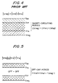
- the relationships between the threshold voltages of these transistors, the ground potential V DD , and the power source potential V reg in this case are shown graphically in Fig. 4.
- V TP > V G(t) > V TN both transistors are turned on and a short-circuiting period is established thereby.
- the threshold voltages of the transistors 42 and 52 in this embodiment are set in such a manner that the above Equations (2) and (3) are satisfied.
- the relationships between the threshold voltages, the ground potential V DD , and the power source potential V reg in this case are shown in Fig. 5. That is to say, if the value of the feedback input V G(t) to the inverting amplifier 30 is set to be within the following range with respect to the potentials of the threshold voltages V TP and V TN : V TN > V G(t) > V TP the two transistors 42 and 52 are turned off firmly so that there is no common-on time during which both of the transistors 42 and 52 are on, as there is in the prior art.
- this method of countering the short-circuiting current of the inverting amplifier 30 of this embodiment can be implemented without increasing the number of circuit components.
- the absolute values of the threshold voltages of the transistors 42 and 52 of this embodiment are each set to be less than the absolute value of the power voltage V reg , as shown by Equations (3). This makes it possible to implement reduced power consumption while maintaining a stable oscillation of the crystal oscillation circuit.
- the absolute value of the amplitude of the feedback signal V G(t) of the inverting amplifier 30 in the crystal oscillation circuit does not exceed the absolute value of the power voltage V reg of the inverting amplifier.
- the transistors 42 and 52 can be driven to turn on and off alternately in a stable manner by setting the absolute values of the threshold voltages of the transistors 42 and 52 to satisfy Equations (3).
- the off-leakage currents of the transistors 42 and 52 in this embodiment are reduced, for reasons that will be described below, making it possible to further reduce the power consumption of the entire circuit.
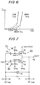
- FIG. 6 A characteristic graph of the relationship between the drain current I D of an enhancement-mode transistor and the voltage V GS between the gate and source thereof is shown in Fig. 6. It can be seen from this graph that the I D -V GS characteristic curve of an enhancement-mode transistor shifts towards the left and the off-leakage current thereof increases, as shown by the broken lines in the figure, as the threshold voltage is made lower (in this graph, the transistor turns off when V GS is equal to or less than the threshold voltage V TH , but at this region, the current I D is yet to flow through the transistor as the off-leakage current, as shown by the broken lines in the figure).
- the threshold voltages of the transistors 42 and 52 are set to be low, as in the prior-art oscillation circuit, the off-leakage current at and below the threshold voltage is larger, and the power consumption is increased by that amount.
- the OFF region for the Pch-transistor 42 is then defined as regions 1000 and 1100 of V GP ⁇ V TP shown in Fig. 9, which satisfy the following formula (a):
- V GSP V GP ⁇ V TP
- the ON region becomes a region 2000 of V GP ⁇ V TP .
- the sub-threshold region 1100 forming a part of the OFF region will be described.
- the conduction type of the silicon crystal surface is only slightly inverted. If there is a gradient in the carrier density, the carriers diffuse from one region having a high density to another region having a low density, so that the drain current I D (OFF current in transistor) flows through the OFF region.
- I D OFF current in transistor
- the region 1100 through which such a drain current flows is called a sub-threshold region and forms a part of the OFF region.
- the OFF region for the Nch-transistor 52 is similar to that for the Pch-transistor 42 and will not further be described herein.
- the value Q is equal to or higher than 10,000.
- the threshold voltages V TP and V TN of the transistors 42 and 52 should not be reduced.
- the constant voltage V reg should be reduced to its lower limit. V reg ⁇ V TP + V TN V reg > V TP , V reg > V TN
- the drain current I D at the sub-threshold region 1100 increases exponentially when the threshold voltage decreases as it is apparent from the formula (c). Therefore, it is undesirable to reduce the threshold voltage.
- Figs. 11 and 12 show the changes in only the V reg .
- the relationship between V reg1 and V reg2 in Figs. 11 and 12 is V reg1 > V reg2 .
- the threshold voltage is the same in Figs. 11 and 12).
- a curve V G - I D is shifted in a direction of arrow 3000 when V reg decreases.
- the constant and threshold voltages may vary among oscillation circuits that are produced in large quantities.
- the constant voltage V reg2 may be reduced to a level lower than the target level and the threshold voltages V TP and V TN may exceed the target levels.
- the drain current at the sub - threshold region may too be reduced making oscillation unstable.
- this embodiment uses such an arrangement of circuit as shown in Fig. 1.
- the circuit supplies an additional current from constant current sources 600 and 610 connected in parallel to the respective transistors 42 and 52, in order to offset a shortage of power necessary for stabilizing oscillation caused by the reduction of the drain current I D at the sub-threshold region due to the fluctuations of the constant voltages in oscillation circuits produced in great quantities.
- the operating current at the sub-threshold region becomes equal to the sum of the sub-threshold current I D of the transistor 52 and the current I2 of the constant current source 610.
- the Pch-transistor 42 conversely, the operating current at the sub-threshold region becomes equal to the sum of the sub-threshold current I D of the transistor 42 and the current I1 of the constant current source 600.
- oscillation may be stabilized even though the actual value V reg becomes smaller than the target value V reg-A set in the designing process due to the fluctuations of the constant voltages in oscillation circuits that are produced in large quantities. Furthermore, oscillation may be stabilized even though the values V TP and V TN are increased to reduce the drain current at the sub-threshold region.
- V reg may be increased or V TP and V TN may be reduced.
- the drain current at the sub-threshold region may be sufficiently high, so that the currents from the constant current sources 600 and 610 become unnecessary for stable oscillation.
- the constant voltage V reg may be higher than the target level V reg-A resulting in excess power supply. In such a case, even though all the constant currents are cut off, it is impossible to reduce the power consumption.
- the present embodiment designs a product so that the target constant voltage is equal to V reg-B , for example, as shown in Fig. 14B.
- the target constant voltage V reg-B is set to be between the absolute value of the minimum constant voltage required for stable oscillation and the absolute value of the first constant voltage V reg-MIN smaller than the absolute value of said minimum constant voltage by the range of fluctuations ⁇ V reg of the constant voltages in oscillation circuits which are produced in large quantities.
- the present embodiment takes an arrangement for supplying an additional current from the constant current sources 600 and 610 connected in parallel to the respective transistors 42 and 52, in order to offset a shortage of power necessary for stabilizing oscillation.
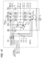
- the present embodiment takes an arrangement of circuit shown in Fig. 13 so as to fully deal with fluctuations of the constant voltages V reg in oscillation circuits, which are produced in large quantities.
- the product for example, such that the target constant voltage V reg-B is set to be between the absolute value of the minimum constant voltage required for stabilizing oscillation and the absolute value of the first constant voltage V reg-MIN smaller than the absolute value of said minimum constant voltage by the range of fluctuations ⁇ V reg of the constant voltages in oscillation circuits which are produced in great quantities as shown in Fig. 14B.
- an oscillation circuit comprises a plurality of constant current sources 600-1, 600-2, 600-3, 610-1, 610-2 and 610-3 and a selection circuit for selecting one of the constant current sources.
- the current value in a constant current source that may stabilize oscillation is optimized during the IC producing step (inspection step) to provide the circuit shown in Fig. 1.
- a transistor 42 is connected in parallel to the first group of constant current sources 600-1, 600-2 and 600-3 while a transistor 52 is connected in parallel to the second group of constant current sources 610-1, 610-2 and 600-3.
- the selection circuit comprises constant current source selection switching elements 602-1, 602-2, 602-3, 612-1, 612-2 and 612-3, each of which is connected in series to the respective one of the transistors 600-1, 600-2, 600-3, 610-1, 610-2 and 610-3.
- a storage circuit 620 receives either of external input signals IN1, IN2 and IN3. The storage circuit 620 responds to the received external input signals to selectively output the corresponding one of said three selection signals SEL1, SEL2 and SEL3.
- Each of the three selection signals SEL1, SEL2 and SEL3 output from the storage circuit 620 is then input into the corresponding one of the switching elements 602-1, 602-2 and 602-3 and also into the gate of the corresponding one of the switching elements 612-1, 612-2 and 612-3 through the corresponding one of inverters 614-1, 614-2 and 614-3.
- the selection signal SEL1 is output, a pair of transistors 602-1 and 612-1 are turned on and a pair of constant current sources 600-1 and 610-1 are selected.
- the constant currents from the constant current sources 600-1, 600-2, 600-3, 610-1, 610-2 and 610-3 are set as follows:
- the drain current I D at the sub-threshold region is first measured.
- an external signal for selecting a constant current source for supplying an additional current is input into the storage circuit 620.
- the current value of the constant current source required for stable oscillation is optimized against fluctuations of the constant voltages in oscillation circuits which are produced in large quantities.
- the circuit of Fig. 13 may select one of eight combinations of constant current sources 600 and 610. Further, three external input signals may be added so that the circuit may use six external input signals for individually selecting each of the constant current sources 600 and 610. (This is because the values V TP and V TN do not fluctuate in a single direction in oscillation circuits which are produced in large quantities.)
- Figs. 1 and 13 are similar for having the constant current sources 600 and 610, but are different from each other in the drain current characteristics at the sub-threshold regions of the Pch- and Nch-transistors depending on the IC producing process.
- an additional current required for stable oscillation may be supplied from either of the constant current source 600 or 610, if necessary.
- the above embodiments have been described as to the oscillation circuit which comprises a plurality of constant current sources, each of which can be in turn selected during the IC inspection process.
- the oscillation circuit may only include a single constant current source, the capacity of which can be adjusted during the IC inspection process.
- the back-gate effect in FET forming the constant current source may be utilized to change the threshold value in FET for controlling the value of the constant current supplied as the drain current.
- the storage circuit 620 may be formed by EEPROM, ferroelectric memory, non-volatile memory, FUSE and laser-cutting type memory or the like.
- V TP ⁇ V TN the voltages for initiating and terminating oscillation may be reduced while satisfying the formulae (2) and (3).
- the first and second embodiments have been described above as being configured in such a manner that the threshold voltages of the transistors 42 and 52 satisfy Equation (2) to reduce the short-circuiting current, by way of example.
- the present embodiment of the invention makes it possible to reduce the short-circuiting current of the inverting amplifier 30 in a manner similar to that of the first embodiment, by applying direct current (DC) bias voltages to the gates of the transistors 42 and 52, even when those transistors 42 and 52 are configured to satisfy the condition of Equation (1), as in the prior art.
- DC direct current
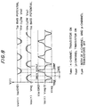
- the crystal oscillation circuit of this embodiment is shown in Fig. 7 and a timing chart thereof is shown in Fig. 8.
- the arrangements of the constant current sources 600 and 610 and that of a selection circuit for selecting a constant current source as well as other arrangements described in the first and second embodiments are applicable to the present embodiment and therefore will not be discussed herein.
- This crystal oscillation circuit comprises a first bias circuit 70 and a second bias circuit 80 that each cause a shift in the DC potential of the feedback input V G(t) of the inverting amplifier 30 that is input to the gates of the transistors 42 and 52.
- bias circuits 70 and 80 each comprises a capacitor 72 or 82 for removing the DC component, and a resistor 74 or 84 for applying a DC bias voltage.
- the capacitors 72 and 82 are used to remove the DC component from the gate signal V G(t) and apply the resultant signal to the gates of the corresponding transistors 42 and 52.
- the resistor 74 is connected between the gate of the transistor 42 and the ground potential V DD , to pull the DC potential of the feedback input V G(t) that is input to the gate of the transistor 42 up to the ground potential V DD .
- the resistor 84 is connected between the gate of the transistor 52 and the power voltage V reg , to pull the DC potential of the feedback input V G(t) that is input to the gate of the transistor 52 down to the power source potential V reg .
- the above configuration ensures that the gate signal V G(t) that is input as feedback to the inverting amplifier 30 is applied to the gates of the transistors 42 and 52 in states in which the DC potential thereof has been converted to V DD and the power source potential V reg by the first and second bias circuits 70 and 80, as indicated by V GP(t) and V GN(t) .
- this embodiment makes it possible to reduce the short-circuiting currents even when the absolute values of the threshold voltages of the enhancement-mode transistors 42 and 52 are made smaller. As a result, the power voltage applied to the inverting amplifier 30 is smaller, which also helps to make it possible to reduce the power consumption.
- bias voltages applied to the first and second bias circuits 70 and 80 could equally well be shifted in such a manner that the DC potentials of the feedback inputs to the gates of the transistors 42 and 52 are at potentials other than those of this embodiment, provided that the transistors 42 and 52 are not on simultaneously.
- each of the first and second circuits 40 and 50 had a single transistor, by way of example, but other configurations could be devised in which other circuit elements could be incorporated into the circuits if necessary, without causing any loss of function of the first and second circuits 40 and 50.
- a semiconductor device is fabricated to comprise the crystal oscillation circuit of the above embodiments, or an electronic circuit that comprises such a crystal oscillation circuit, and this semiconductor device could be mounted in portable electronic equipment that has a restricted power source capacity, such as a portable telephone, a portable computer terminal, or any other type of portable equipment.
- the descriptions of the above embodiments are based on the use of the crystal oscillation circuit in an electronic circuit for a timepiece, by way of example, but the present invention is not limited thereto. It has many other applications and is extremely effective when used in a wide range of portable electronic equipment that have restricted power source capacities, such as portable telephones, portable computer terminals, or any other type of portable equipment.
- the embodiments have been described as to the crystal oscillation circuit having the crystal oscillator as a source of oscillation.
- the present invention may be applied similarly to a drive circuit (or driver) such as a piezoelectric motor which uses a piezoelectric element as an oscillator.
Landscapes
- Chemical & Material Sciences (AREA)
- Crystallography & Structural Chemistry (AREA)
- Oscillators With Electromechanical Resonators (AREA)
- Electric Clocks (AREA)
Applications Claiming Priority (2)
| Application Number | Priority Date | Filing Date | Title |
|---|---|---|---|
| JP2000183384A JP3940879B2 (ja) | 2000-06-19 | 2000-06-19 | 発振回路、電子回路、半導体装置、電子機器および時計 |
| JP2000183384 | 2000-06-19 |
Publications (4)
| Publication Number | Publication Date |
|---|---|
| EP1176719A2 true EP1176719A2 (fr) | 2002-01-30 |
| EP1176719A3 EP1176719A3 (fr) | 2003-04-23 |
| EP1176719B1 EP1176719B1 (fr) | 2010-09-15 |
| EP1176719B8 EP1176719B8 (fr) | 2010-10-27 |
Family
ID=18683977
Family Applications (1)
| Application Number | Title | Priority Date | Filing Date |
|---|---|---|---|
| EP01113644A Expired - Lifetime EP1176719B8 (fr) | 2000-06-19 | 2001-06-19 | Circuit d'oscillateur, circuit électronique, dispositif semi-conducteur, appareil électronique et pièce d'horlogerie |
Country Status (5)
| Country | Link |
|---|---|
| EP (1) | EP1176719B8 (fr) |
| JP (1) | JP3940879B2 (fr) |
| CN (1) | CN1149454C (fr) |
| DE (1) | DE60143067D1 (fr) |
| HK (1) | HK1041571A1 (fr) |
Cited By (1)
| Publication number | Priority date | Publication date | Assignee | Title |
|---|---|---|---|---|
| GB2380076A (en) * | 2001-07-24 | 2003-03-26 | Henry Clinton | Apparatus for the high voltage testing of insulated conductors and oscillator circuit for use with same |
Families Citing this family (5)
| Publication number | Priority date | Publication date | Assignee | Title |
|---|---|---|---|---|
| JP5939852B2 (ja) * | 2012-03-22 | 2016-06-22 | エスアイアイ・セミコンダクタ株式会社 | アナログ電子時計 |
| JP6385208B2 (ja) * | 2014-09-03 | 2018-09-05 | エイブリック株式会社 | 水晶発振回路及び電子時計 |
| FR3026631B1 (fr) | 2014-10-03 | 2016-12-09 | Ecole Polytech | Dispositif medical implantable muni de capteurs |
| FR3049843A1 (fr) * | 2016-04-06 | 2017-10-13 | Instent | Dispositif medical muni de capteurs |
| US11736066B2 (en) * | 2021-12-22 | 2023-08-22 | Realtek Semiconductor Corporation | Oscillation circuit and method of automatic duty cycle calibration |
Family Cites Families (3)
| Publication number | Priority date | Publication date | Assignee | Title |
|---|---|---|---|---|
| US3979698A (en) * | 1973-10-19 | 1976-09-07 | Itt Industries, Inc. | Crystal oscillator circuit |
| US6046648A (en) * | 1996-12-27 | 2000-04-04 | Seiko Epson Corporation | Crystal oscillator circuit having low power consumption |
| US6097257A (en) * | 1997-01-22 | 2000-08-01 | Seiko Epson Corporation | Crystal oscillator circuit having transistor with back gate voltage control |
-
2000
- 2000-06-19 JP JP2000183384A patent/JP3940879B2/ja not_active Expired - Fee Related
-
2001
- 2001-06-19 DE DE60143067T patent/DE60143067D1/de not_active Expired - Lifetime
- 2001-06-19 EP EP01113644A patent/EP1176719B8/fr not_active Expired - Lifetime
- 2001-06-19 CN CNB011221925A patent/CN1149454C/zh not_active Expired - Fee Related
-
2002
- 2002-04-29 HK HK02103173.1A patent/HK1041571A1/en unknown
Cited By (2)
| Publication number | Priority date | Publication date | Assignee | Title |
|---|---|---|---|---|
| GB2380076A (en) * | 2001-07-24 | 2003-03-26 | Henry Clinton | Apparatus for the high voltage testing of insulated conductors and oscillator circuit for use with same |
| GB2380076B (en) * | 2001-07-24 | 2004-11-17 | Henry Clinton | Apparatus for the high voltage testing of insulated conductors and oscillator circuit for use with same |
Also Published As
| Publication number | Publication date |
|---|---|
| EP1176719B8 (fr) | 2010-10-27 |
| JP3940879B2 (ja) | 2007-07-04 |
| CN1149454C (zh) | 2004-05-12 |
| DE60143067D1 (de) | 2010-10-28 |
| EP1176719A3 (fr) | 2003-04-23 |
| JP2002009550A (ja) | 2002-01-11 |
| EP1176719B1 (fr) | 2010-09-15 |
| CN1329290A (zh) | 2002-01-02 |
| HK1041571A1 (en) | 2002-07-12 |
Similar Documents
| Publication | Publication Date | Title |
|---|---|---|
| EP1523806B1 (fr) | Oscillateur en anneau avec stabilisation de frequence | |
| US5126695A (en) | Semiconductor integrated circuit device operated with an applied voltage lower than required by its clock oscillator | |
| EP0936736B1 (fr) | Eléments à retard pour un oscillateur commandé par un signal | |
| US20160065220A1 (en) | Cmos oscillator having stable frequency with process, temperature, and voltage variation | |
| US20090128992A1 (en) | Mos capacitor structure and linearization method for reduced variation of the capacitance | |
| US11165433B2 (en) | Charge pump, PLL circuit, and oscillator | |
| US7612623B2 (en) | Micropower RC oscillator | |
| US7183868B1 (en) | Triple inverter pierce oscillator circuit suitable for CMOS | |
| US20190139616A1 (en) | Shift register, array substrate and display device | |
| US3889211A (en) | MOS field effect transistor crystal oscillator | |
| EP0851323B1 (fr) | Circuit oscillateur, circuit électronique utilisant celui-ci, et dispositif sémi-conducteur, appareil électronique, et pièce d'horlogerie utilisant celui-ci | |
| US6411169B1 (en) | Oscillation circuit, electronic circuit using the same, and semiconductor device, electronic equipment, and timepiece using the same | |
| JP2001274676A (ja) | レベルシフト回路および画像表示装置 | |
| JPS6259924B2 (fr) | ||
| US6359814B1 (en) | Negative output voltage charge pump and method therefor | |
| EP1176719B1 (fr) | Circuit d'oscillateur, circuit électronique, dispositif semi-conducteur, appareil électronique et pièce d'horlogerie | |
| JP2007110504A (ja) | 半導体集積回路装置 | |
| US7495497B1 (en) | Temperature compensated integrated circuits | |
| US4255723A (en) | Amplitude control inverter circuit for electronic device | |
| US10868495B2 (en) | Auto-compensation for control voltage range of VCO at low power supply | |
| KR20160012560A (ko) | 딜레이 셀 및 이를 적용하는 지연 동기 루프 회로와 위상 동기 루프 회로 | |
| US10747248B2 (en) | Oscillator | |
| GB2084421A (en) | Oscillator Circuit With Low Current Consumption | |
| JP6385176B2 (ja) | アナログ電子時計 | |
| JP2003524305A (ja) | 温度補償発振器 |
Legal Events
| Date | Code | Title | Description |
|---|---|---|---|
| PUAI | Public reference made under article 153(3) epc to a published international application that has entered the european phase |
Free format text: ORIGINAL CODE: 0009012 |
|
| AK | Designated contracting states |
Kind code of ref document: A2 Designated state(s): AT BE CH CY DE DK ES FI FR GB GR IE IT LI LU MC NL PT SE TR |
|
| AX | Request for extension of the european patent |
Free format text: AL;LT;LV;MK;RO;SI |
|
| PUAL | Search report despatched |
Free format text: ORIGINAL CODE: 0009013 |
|
| AK | Designated contracting states |
Designated state(s): AT BE CH CY DE DK ES FI FR GB GR IE IT LI LU MC NL PT SE TR |
|
| AX | Request for extension of the european patent |
Extension state: AL LT LV MK RO SI |
|
| 17P | Request for examination filed |
Effective date: 20030904 |
|
| AKX | Designation fees paid |
Designated state(s): CH DE FR GB LI |
|
| 17Q | First examination report despatched |
Effective date: 20080429 |
|
| GRAP | Despatch of communication of intention to grant a patent |
Free format text: ORIGINAL CODE: EPIDOSNIGR1 |
|
| GRAS | Grant fee paid |
Free format text: ORIGINAL CODE: EPIDOSNIGR3 |
|
| GRAA | (expected) grant |
Free format text: ORIGINAL CODE: 0009210 |
|
| AK | Designated contracting states |
Kind code of ref document: B1 Designated state(s): CH DE FR GB LI |
|
| REG | Reference to a national code |
Ref country code: GB Ref legal event code: FG4D Ref country code: CH Ref legal event code: EP |
|
| REG | Reference to a national code |
Ref country code: CH Ref legal event code: PK |
|
| RBV | Designated contracting states (corrected) |
Designated state(s): DE FR GB |
|
| REF | Corresponds to: |
Ref document number: 60143067 Country of ref document: DE Date of ref document: 20101028 Kind code of ref document: P |
|
| REG | Reference to a national code |
Ref country code: CH Ref legal event code: PK Free format text: DER EINTRAG DES WIDERRUF DER ERTEILUNG DURCH DAS EPA ERFOLGTE IRRTUEMLICH. DAS PATENT WURDE AM 15.09.2010 ERTEILT. DIE BENENNUNG CH/LI WURDE VOR DER ER |
|
| REG | Reference to a national code |
Ref country code: HK Ref legal event code: WD Ref document number: 1041571 Country of ref document: HK |
|
| PLBE | No opposition filed within time limit |
Free format text: ORIGINAL CODE: 0009261 |
|
| STAA | Information on the status of an ep patent application or granted ep patent |
Free format text: STATUS: NO OPPOSITION FILED WITHIN TIME LIMIT |
|
| 26N | No opposition filed |
Effective date: 20110616 |
|
| REG | Reference to a national code |
Ref country code: DE Ref legal event code: R097 Ref document number: 60143067 Country of ref document: DE Effective date: 20110616 |
|
| REG | Reference to a national code |
Ref country code: DE Ref legal event code: R073 Ref document number: 60143067 Country of ref document: DE |
|
| REG | Reference to a national code |
Ref country code: DE Ref legal event code: R073 Ref document number: 60143067 Country of ref document: DE |
|
| REG | Reference to a national code |
Ref country code: DE Ref legal event code: R074 Ref document number: 60143067 Country of ref document: DE |
|
| REG | Reference to a national code |
Ref country code: DE Ref legal event code: R119 Ref document number: 60143067 Country of ref document: DE Effective date: 20120103 |
|
| REG | Reference to a national code |
Ref country code: DE Ref legal event code: R074 Ref document number: 60143067 Country of ref document: DE Effective date: 20120407 |
|
| REG | Reference to a national code |
Ref country code: FR Ref legal event code: PLFP Year of fee payment: 15 |
|
| PGFP | Annual fee paid to national office [announced via postgrant information from national office to epo] |
Ref country code: GB Payment date: 20150617 Year of fee payment: 15 Ref country code: DE Payment date: 20150616 Year of fee payment: 15 |
|
| PGFP | Annual fee paid to national office [announced via postgrant information from national office to epo] |
Ref country code: FR Payment date: 20150608 Year of fee payment: 15 |
|
| REG | Reference to a national code |
Ref country code: DE Ref legal event code: R119 Ref document number: 60143067 Country of ref document: DE |
|
| GBPC | Gb: european patent ceased through non-payment of renewal fee |
Effective date: 20160619 |
|
| REG | Reference to a national code |
Ref country code: FR Ref legal event code: ST Effective date: 20170228 |
|
| PG25 | Lapsed in a contracting state [announced via postgrant information from national office to epo] |
Ref country code: FR Free format text: LAPSE BECAUSE OF NON-PAYMENT OF DUE FEES Effective date: 20160630 Ref country code: DE Free format text: LAPSE BECAUSE OF NON-PAYMENT OF DUE FEES Effective date: 20170103 |
|
| PG25 | Lapsed in a contracting state [announced via postgrant information from national office to epo] |
Ref country code: GB Free format text: LAPSE BECAUSE OF NON-PAYMENT OF DUE FEES Effective date: 20160619 |