EP1176807A1 - Unterabtastung von Bildsensoren mit geneigtem Farbfiltermuster - Google Patents
Unterabtastung von Bildsensoren mit geneigtem Farbfiltermuster Download PDFInfo
- Publication number
- EP1176807A1 EP1176807A1 EP01109924A EP01109924A EP1176807A1 EP 1176807 A1 EP1176807 A1 EP 1176807A1 EP 01109924 A EP01109924 A EP 01109924A EP 01109924 A EP01109924 A EP 01109924A EP 1176807 A1 EP1176807 A1 EP 1176807A1
- Authority
- EP
- European Patent Office
- Prior art keywords
- sub
- read
- sampling
- skewed
- rows
- Prior art date
- Legal status (The legal status is an assumption and is not a legal conclusion. Google has not performed a legal analysis and makes no representation as to the accuracy of the status listed.)
- Withdrawn
Links
- 238000005070 sampling Methods 0.000 title claims abstract description 97
- 238000003384 imaging method Methods 0.000 claims abstract description 44
- 238000000034 method Methods 0.000 claims abstract description 12
- 230000008569 process Effects 0.000 claims description 5
- 230000035945 sensitivity Effects 0.000 abstract description 5
- 238000012545 processing Methods 0.000 description 17
- 230000005855 radiation Effects 0.000 description 15
- 239000000758 substrate Substances 0.000 description 11
- 239000011159 matrix material Substances 0.000 description 6
- 238000003491 array Methods 0.000 description 4
- 230000006870 function Effects 0.000 description 3
- 239000004065 semiconductor Substances 0.000 description 3
- 230000015556 catabolic process Effects 0.000 description 2
- 238000006731 degradation reaction Methods 0.000 description 2
- 238000010586 diagram Methods 0.000 description 2
- 238000009792 diffusion process Methods 0.000 description 2
- 239000000463 material Substances 0.000 description 2
- 238000012986 modification Methods 0.000 description 2
- 230000004048 modification Effects 0.000 description 2
- 239000007787 solid Substances 0.000 description 2
- 238000012935 Averaging Methods 0.000 description 1
- 239000003990 capacitor Substances 0.000 description 1
- 238000006243 chemical reaction Methods 0.000 description 1
- 239000003086 colorant Substances 0.000 description 1
- 230000000295 complement effect Effects 0.000 description 1
- 238000010276 construction Methods 0.000 description 1
- 230000005684 electric field Effects 0.000 description 1
- 230000002349 favourable effect Effects 0.000 description 1
- 239000003574 free electron Substances 0.000 description 1
- 238000004519 manufacturing process Methods 0.000 description 1
- 229910044991 metal oxide Inorganic materials 0.000 description 1
- 150000004706 metal oxides Chemical class 0.000 description 1
- 230000003287 optical effect Effects 0.000 description 1
- 230000003071 parasitic effect Effects 0.000 description 1
- 238000001454 recorded image Methods 0.000 description 1
- 230000001360 synchronised effect Effects 0.000 description 1
- 238000012546 transfer Methods 0.000 description 1
- 230000009466 transformation Effects 0.000 description 1
Images




Classifications
-
- H—ELECTRICITY
- H04—ELECTRIC COMMUNICATION TECHNIQUE
- H04N—PICTORIAL COMMUNICATION, e.g. TELEVISION
- H04N25/00—Circuitry of solid-state image sensors [SSIS]; Control thereof
- H04N25/70—SSIS architectures; Circuits associated therewith
- H04N25/76—Addressed sensors, e.g. MOS or CMOS sensors
- H04N25/7795—Circuitry for generating timing or clock signals
-
- H—ELECTRICITY
- H04—ELECTRIC COMMUNICATION TECHNIQUE
- H04N—PICTORIAL COMMUNICATION, e.g. TELEVISION
- H04N25/00—Circuitry of solid-state image sensors [SSIS]; Control thereof
- H04N25/40—Extracting pixel data from image sensors by controlling scanning circuits, e.g. by modifying the number of pixels sampled or to be sampled
- H04N25/44—Extracting pixel data from image sensors by controlling scanning circuits, e.g. by modifying the number of pixels sampled or to be sampled by partially reading an SSIS array
- H04N25/445—Extracting pixel data from image sensors by controlling scanning circuits, e.g. by modifying the number of pixels sampled or to be sampled by partially reading an SSIS array by skipping some contiguous pixels within the read portion of the array
-
- H—ELECTRICITY
- H04—ELECTRIC COMMUNICATION TECHNIQUE
- H04N—PICTORIAL COMMUNICATION, e.g. TELEVISION
- H04N23/00—Cameras or camera modules comprising electronic image sensors; Control thereof
- H04N23/10—Cameras or camera modules comprising electronic image sensors; Control thereof for generating image signals from different wavelengths
- H04N23/11—Cameras or camera modules comprising electronic image sensors; Control thereof for generating image signals from different wavelengths for generating image signals from visible and infrared light wavelengths
-
- H—ELECTRICITY
- H04—ELECTRIC COMMUNICATION TECHNIQUE
- H04N—PICTORIAL COMMUNICATION, e.g. TELEVISION
- H04N25/00—Circuitry of solid-state image sensors [SSIS]; Control thereof
- H04N25/10—Circuitry of solid-state image sensors [SSIS]; Control thereof for transforming different wavelengths into image signals
- H04N25/11—Arrangement of colour filter arrays [CFA]; Filter mosaics
- H04N25/13—Arrangement of colour filter arrays [CFA]; Filter mosaics characterised by the spectral characteristics of the filter elements
- H04N25/134—Arrangement of colour filter arrays [CFA]; Filter mosaics characterised by the spectral characteristics of the filter elements based on three different wavelength filter elements
-
- H—ELECTRICITY
- H04—ELECTRIC COMMUNICATION TECHNIQUE
- H04N—PICTORIAL COMMUNICATION, e.g. TELEVISION
- H04N25/00—Circuitry of solid-state image sensors [SSIS]; Control thereof
- H04N25/40—Extracting pixel data from image sensors by controlling scanning circuits, e.g. by modifying the number of pixels sampled or to be sampled
- H04N25/44—Extracting pixel data from image sensors by controlling scanning circuits, e.g. by modifying the number of pixels sampled or to be sampled by partially reading an SSIS array
- H04N25/447—Extracting pixel data from image sensors by controlling scanning circuits, e.g. by modifying the number of pixels sampled or to be sampled by partially reading an SSIS array by preserving the colour pattern with or without loss of information
-
- H—ELECTRICITY
- H04—ELECTRIC COMMUNICATION TECHNIQUE
- H04N—PICTORIAL COMMUNICATION, e.g. TELEVISION
- H04N25/00—Circuitry of solid-state image sensors [SSIS]; Control thereof
- H04N25/70—SSIS architectures; Circuits associated therewith
-
- H—ELECTRICITY
- H04—ELECTRIC COMMUNICATION TECHNIQUE
- H04N—PICTORIAL COMMUNICATION, e.g. TELEVISION
- H04N25/00—Circuitry of solid-state image sensors [SSIS]; Control thereof
- H04N25/70—SSIS architectures; Circuits associated therewith
- H04N25/71—Charge-coupled device [CCD] sensors; Charge-transfer registers specially adapted for CCD sensors
- H04N25/74—Circuitry for scanning or addressing the pixel array
-
- H—ELECTRICITY
- H04—ELECTRIC COMMUNICATION TECHNIQUE
- H04N—PICTORIAL COMMUNICATION, e.g. TELEVISION
- H04N25/00—Circuitry of solid-state image sensors [SSIS]; Control thereof
- H04N25/70—SSIS architectures; Circuits associated therewith
- H04N25/76—Addressed sensors, e.g. MOS or CMOS sensors
-
- H—ELECTRICITY
- H04—ELECTRIC COMMUNICATION TECHNIQUE
- H04N—PICTORIAL COMMUNICATION, e.g. TELEVISION
- H04N25/00—Circuitry of solid-state image sensors [SSIS]; Control thereof
- H04N25/70—SSIS architectures; Circuits associated therewith
- H04N25/76—Addressed sensors, e.g. MOS or CMOS sensors
- H04N25/78—Readout circuits for addressed sensors, e.g. output amplifiers or A/D converters
Definitions
- the present invention relates to solid-state imaging devices and, more particularly, to an active pixel sensor sub-sampling architecture for such imaging devices.
- a typical CCD imager includes a matrix of photosites (an array) that are capable of collecting free electrons that form an electrical charge packet that is directly proportional to the photon radiation incident at that photosite. Accordingly, when an image is focused on the surface of the array, the charge packet at each photosite of the array corresponds to a respective picture element or pixel of the complete image.
- the generated photosite charge packets are transferred in a parallel manner into a CCD shift register where they are transferred serially as an output signal of the CCD image.
- the CCD imager output signal is a series of electronic signals whose amplitude represent the light intensity of the image at each pixel for a single image frame. The process can be continuously repeated to generate output signals, which correspond to several image frames per second. Consequently, each frame in the generated output signal contains information concerning the detected light intensity at each photosite.
- CCD imagers require near-perfect charge transfer over a distance of approximately 1-2 centimeters through semiconductor materials. Therefore, such CCD imagers require a substantial amount of power, are difficult to manufacture in large array sizes, and are difficult to integrate with complementary metal oxide semiconductor (CMOS) on-chip electronics.
- CMOS complementary metal oxide semiconductor
- the difficulty is that the standard CCD process is incompatible with CMOS processing, while the imager signal processing electronics required for the imager are best fabricated in CMOS.
- APS active pixel sensors
- APS employ one or more on-chip transistors at each pixel photosite in the array (see U.S. Patents No. 5,471,515 and European Patent application publication 957,630).
- the transistors at the photosite buffer a photo signal corresponding to the charge packet generated by the photosite and drive an output signal line avoiding the disadvantages of the CCD imagers that have to serially shift the data out.
- typical APS arrays still generate an output signal with each frame (representing a row of image data in the array) containing information representing the detected light intensity at each photosite.
- Image sensor pixel arrays are typically sub-sampled to either scale the final image size and aspect ratio, to increase the frame rate over what can be achieved with the maximum resolution, or both.
- One drawback of CCD imaging arrays is that they have very limited capability to perform sub-sampling in the horizontal direction and their ability to increase the frame rate through horizontal sub-sampling is non-existent or extremely limited.
- CMOS image sensors have the capability to randomly access individual pixels, which means that the objective of increasing the nominal frame rate by increasing the sub-sample ratio is possible.
- the degree of degradation is a function of the size and alignment of the individual image features relative to the resolution of the optics and image sensor pixels. It is also a function of the spatial frequency of the samples taken, which is dictated by both the sub-sample ratio and the selected sub-sampling pattern.
- CMOS image sensors are capable of equivalent horizontal and vertical sub-sample ratios and can achieve frame rate increases via sub-sampling.
- CMOS sensors typically perform sub-sampling with the same columns sampled in each row using a rectangular grid sub-sampling pattern.
- the disadvantage of a uniform rectangular grid is that the spatial frequency of the samples is not maximized and the resulting patterns are particularly sensitive to degradation when focused on fine pitched vertical lines such as text.
- An image sensor pixel sub-sampling technique is described that provides fast imaging with improved image spatial resolution.
- the sample pattern for an imaging array is shifted left and right from row to row, to increase the horizontal sampling frequency of the image.
- the skewed sub-sampling reduces the feature size that can be resolved and also reduces angular alignment sensitivity. As a result, the range of images and feature sizes that can be captured within the desired image quality and sensing time thresholds are increased.
- the skewed sub-sampling is performed while sampling the same number of pixels on each row that would be sampled when sub-sampling without shifting the pattern, and is performed at the same rate.
- the option of skewing the pattern can be enabled or disabled, for example, by setting a programmable register bit.
- the skewed sub-sampling technique can be applied to a monochrome imaging array.
- skewed sub-sampling can be employed on a color imaging array, for example, one having a Bayer pattern.
- Figure 1 includes a block diagram of an active pixel sensor array 180 used in the preferred embodiment and its associated circuitry used to control and read out the image that is formed on the array.
- the array 180 is made up of rows and columns of active pixel sensor sites (APS) 10.
- APS active pixel sensor sites
- the preferred embodiment of the invention employs a skewed-pattern pixel sub-sampling technique to provide fast imaging with improved image spatial resolution when image signal 170 is created by selectively sub-sampling APS sites 10 of active pixel sensor array 180.
- 4 rows and 4 columns of sensor sites 10 are shown. However, those skilled in the art will appreciated that the number of rows and the numbers of columns could be any size and still meet the scope of the invention.
- timing controller 100 selectively controls row decoder 110, column amplifiers 130 and steering logic 140 to sample some or all of the APS sites 10 of pixel sensor array 180.
- Timing controller 100 generates row control signals 160 to select a particular row of array 180 for sensing.
- Timing controller 100 also generates column control signals 170 to select pixels 10 within the selected row of array 180 for sensing.
- the respective column amplifiers 130 are each driven to a level proportional to the incident light striking the selected pixel in that column of the selected row. The incident light is integrated over an exposure period to adjust to ambient lighting conditions.
- the selected column amplifier 130 outputs are sequentially selected to provide the analog image signal 118.
- Analog-to-digital converter 170 converts analog image signal 118 to digital image signal 170.
- all of the column amplifiers 130 are identical sample and hold amplifiers utilizing the same control signals, bias voltages, and a reference voltage.
- the amplifying element in each column amplifier can be a simple two transistor amplifier or a more complex configuration to provide higher gains with lower power consumption at higher frequencies, thus allowing faster readout rates.
- phase 1) select a row in the array, sample and store the image signal from the pixel in the selected row coupled to the common column line which is coupled to the column amplifier; phase 2) sample and store the reset state of the selected pixel and subtract from its stored sampled image signal; phase 3) present the output of the column amplifier 130 output line when selected to form image data to be processed further by other system electronics on an integrated circuit.
- FIG 2 illustrates one type of an active pixel sensor (APS) site 10, which represents one pixel in the imaging array. This site performs the light to electrical signal transformation.
- An active pixel sensor array is a matrix of this APS site 10 formed in rows and columns (see Figure 1). These APS sites 10 are fabricated on a semiconductor substrate 20, an exemplary type being a P+ substrate shown in Figure 2.
- a photo well 24 is formed in the substrate and is designed to prevent leakage of non-photo generated charge into substrate 20.
- a thin P- epitaxial layer 16 (epi) is formed on top of the P+ substrate 20 to further reduce this leakage.
- the photowell 24, shown in Figure 2 is made of an N+ material to form a diffusion node.
- a contact 26 couples the photo well 24 to other circuitry used to control and convert the light source 22 striking the photo well 24.
- the photo well 24 (a diffusion node) is a reversed biased diode (commonly known as a photodiode), which includes a parasitic capacitor which can store charge 28, thus creating a voltage potential.
- This stored charge 28 is supplied from power supply 46 (Vdd) by a reset switch 40, which when activated fills photo well 24 with charge 28.
- Vdd power supply 46
- the reset switch 40 After the reset switch 40 is opened, the light source 22 striking the photo well 24 causes photonic energy from the light source 22 to form a number of electron-hole pairs in both the photowell 24 and the underlying substrate 20.
- the number of electron-hole pairs is a function of the intensity of the received light energy in light source 22.
- the holes formed in photowell 24 diffuse to the junction with the substrate 20 where they are swept into the substrate 20 under the influence of an electric field at the bias junction of photowell 24 and substrate 20.
- the electrons formed in substrate 20 diffuse to the junction of the photowell 24 and substrate 20 where they are swept to photowell 24 and collected at contact 26.
- the voltage at contact 26 is correspondingly reduced.
- the reset switch 40, buffer 32, and row select switch 34 are fabricated preferably as NMOS FET devices. This fact requires that the gate of each transistor be at least one threshold higher than the source of the transistor to turn on the transistor.
- the maximum voltage potential that the photo well 24 will be charged to is one gate threshold (the magnitude of which is determined by the IC process used, typically 0.8V to 1.2V) less than the voltage present on the gate of reset switch 40, an exemplary value being power supply voltage 46, VDD.
- the voltage follower style buffer 32 will cause its source to be one gate threshold below the signal on its gate. Therefore, the maximum signal that the common column line 38 sees is the power supply voltage 46 (Vdd) less two gate threshold voltages. Also, this maximum signal represents when there is no light source 22 striking the photo well. As light source 22 strikes the photo well, the signal level shown on the common column line 38 will decrease at a rate proportional to the light intensity of light source 22, to voltage potential ground on a maximum intensity light source 22.
- timing controller 100 of Figure 1 is used to select which row and which column to read out of the array through row control signals 160 coupled to row decoder 110.
- the timing controller 100 also generates the timing for a set of column amplifiers 130.
- the timing controller either sequentially selects each column for output or can be programmed, to output the columns at different intervals depending on the desired resolution, when, for example, register 105 has been set to enter a sub-sampling mode.
- An example for sub-sampling a half resolution image might be to select every other column and every other row.
- the timing controller 100 can be set to enter a skewed sub-sampling mode.
- the basic idea of horizontal sub-sampled skewing is to shift the horizontal sub-sample pattern right then left on alternating rows to improve the spatial distribution of samples. This allows higher frequency sampling while outputting the same number of pixels at the same frame rate as a sub-sampled sensor that does not support horizontal skewing. It can also be applied to any decimation ratio.
- Skewed sub-sampling increases the spatial distribution of pixels sampled which therefore reduces, for a given set of optics and pixels, the size of the feature which can be sampled at a high enough frequency for a high quality reproduction.
- the spatial distribution provided by skewed sub-sampling also reduces the angular alignment sensitivity to small features. It can do the above while still performing random sampling of the pixels and therefore maximizing the frame rate.
- Non-skewed sub-sampling has been performed before in CCD image sensors.
- CCD sensors have very limited horizontal sub-sampling capabilities and the patterns cannot be skewed without suffering a time penalty.
- Still the scope of the present invention is envisaged to include skewed sub-sampling of CCD sensors. This is because even though it may take longer than non-skewed sub-sampling of CCD sensors, the spatial distribution of the pixels sampled using skewed sub-sampling permits increased resolution of small objects and reduced angular sensitivity to small features.
- Image array sensors are commonly used in solid state cameras and color image sensors are known which comprise a two-dimensional array of sensing cells which is provided with a matrixed pattern of color filters, for example, red, green and blue filters (e.g., filter 12 of Figure 2). Cell outputs corresponding to different colors are demultiplexed at the array output and fed to respective color channels.
- color filters for example, red, green and blue filters (e.g., filter 12 of Figure 2).
- pixel values for each channel can be approximated at each sensor site.
- the red-channel value at a sensor site having a green filter can be approximated by averaging the red-channel values of the nearest sensor sites having a red.
- More sophisticated demosaicing schemes are known which may also be employed. For example, if an edge is detected in the vicinity of a pixel, a neighboring same color-channel colored site may be excluded from the estimate calculation if it lies on the side of the edge opposite from that of the pixel being estimated.
- neighboring sensing cells in the array have different color filters in order to achieve appropriate spatial sampling of radiation of each color being sensed for each color channel of the sensor.
- Adjacent sensing cells in each row may be formed and arranged for sensing radiation of wavelengths corresponding to different ones of a plurality of color channels.
- Each row may, for example, contain three series of sensing cells, for sensing red, green and blue wavelength radiation respectively.
- the three series of cells may be interspersed such that each row contains an alternating pattern of red (R), green (G), and blue (B), sensing cells e.g. R G B R G B R G ...
- each row may, for example, contain only two series of sensing cells.
- the two series of cells in each row may be arranged so that every third cell senses a different color radiation to every first and second cell e.g. B B R B B R B B R...
- An interspersed series of sensing cells contained in any one row may have sensing cells for sensing at least one different color radiation to the sensing cells of the interspersed series of cells in another row.
- a first row may contain two series of cells for sensing red and blue radiation and a second row may contain two series of cells for sensing red and green radiation.
- the matrixed pattern of color filters is a Bayer matrix as described in US patent no. 3,971,065.
- a Bayer matrix is shown schematically in pixel sensor array 180 of Figure 1. Although the skewed sub-sampling will be discussed in the context of the Bayer pattern, it is to be understood that this pattern is used for purpose of example and that other patterns may be employed without departing from the scope of the invention.
- each row of the array has two series of pixels. All of the pixels of each series have the same color of filter and the color filters of the pixels in each series are either red (R), green (G) or blue (B).
- the two series of pixels in each row are interspersed so as to form an alternating two-color pattern e.g. G R G R G R ... etc.
- the first and every subsequent odd-numbered row have the pixel color pattern G R G R G R ... etc.
- the second and every subsequent even-numbered row have the pixel color pattern B G B G B G ... etc.
- the Bayer matrix pixel array pattern shown in Figure 1 has many favorable properties for color image reconstruction. It is known that the human eye is more sensitive to luminance than chrominance, and that green pixels carry the majority of the luminance information. By utilizing the skewed sub-sampling mode to shift the sample pattern left and right from row to row, the horizontal sampling frequency of the image luminance is increased, thus reducing the feature size that can be resolved and reducing the angular alignment sensitivity. As a result, the range of images and feature sizes that can be captured within the desired image quality thresholds are increased. For one embodiment, this is done while sampling the same number of pixels on each row that would be sampled when the pattern is not shifted, and performed at the same rate. Note that the option of skewing the pattern can be enabled or disabled via a programmable register bit, e.g., in register 105 of Figure 1.
- Figures 3A and 3B show details of respective skewed and non-skewed 2:1 sub-sampling patterns of the imaging device shown in Figure 1.
- pixel sensors 10 of pixel sensor array 180 are read in a skewed sub-sampling mode whereby the non-shaded sensors are read and the shaded sensors are not.
- the top, middle and bottom rows form a set of "G-R" rows that have a read sub-set of a G and an adjacent R sensor (forming the top half of a Bayer pattern).
- each G-R series of sensors to be read forms a read sub-set which is separated from another G-R series of sensors to be read by a G-R series of sensors which will not be read (in the 2:1 skewed sub-sampling mode).
- each B-G series of sensors to be read forms a read sub-set which is separated from another B-G series of sensors to be read by a B-G series of sensors which will not be read (in the 2:1 skewed sub-sampling mode).
- the skewing of the sub-sampling pattern is such that for a pair of adjoining rows, a pixel in G-R read sub-set will not have a pixel in a B-G read subset in the same column.
- the G sensor in the left-most column of the top row will be read, but the B sensor directly beneath it in the left-most column will not be read.
- Figure 3B shows details of a non-skewed 2:1 sub-sampling pattern such as might be sampled in a non-skewed sub-sampling mode.
- the non-shaded sensors 10 of array 180 are read and the shaded sensors 10 are not read.
- the sub-sampling pattern is such that for a pair of adjoining rows, a pixel in G-R read sub-set will have a corresponding pixel in a B-G read subset in the same column.
- the G sensor in the left-most column of the top row will be read, and the B sensor directly beneath it in the left-most column will also be read.
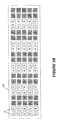
- Figures 4A and 4B show details of respective skewed and non-skewed 4:1 sub-sampling patterns of the imaging device shown in Figure 1.
- pixel sensors 10 of pixel sensor array 180 are read in a skewed sub-sampling mode whereby the non-shaded sensors are read and the shaded sensors are not.
- the top, middle and bottom rows form a set of "G-R" rows that have a read sub-set of a G and an adjacent R sensor (forming the top half of a Bayer pattern).
- each G-R series of sensors to be read forms a read sub-set which is separated from another G-R series of sensors to be read by three G-R series sets of sensors which will not be read (in the 4:1 skewed sub-sampling mode).
- each B-G series of sensors to be read forms a read sub-set which is separated from another B-G series of sensors to be read by three B-G series sets of sensors which will not be read (in the 4:1 skewed sub-sampling mode).
- the skewing of the sub-sampling pattern shown in Figure 4A is such that for a pair of adjoining rows, a pixel in G-R read sub-set will not have a pixel in a B-G read subset in the same column.
- the G sensor in the left-most column of the top row will be read, but the B sensor directly beneath it in the left-most column will not be read.
- whole columns of sensors are not read in Figure 4A because of the higher sub-sampling rate.
- Figure 4B shows details of a non-skewed 4:1 sub-sampling pattern such as might be sampled in a non-skewed sub-sampling mode.
- the non-shaded sensors 10 of array 180 are read and the shaded sensors 10 are not read.
- the sub-sampling pattern is such that for a pair of adjoining rows, a pixel in the G-R read sub-set will have a corresponding pixel in a B-G read subset in the same column.
- the G sensor in the left-most column of the top row will be read, and the B sensor directly beneath it in the left-most column will also be read.
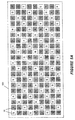
- Figures 5A and 5B show details of alternative skewed sub-sampling patterns of the imaging device shown in Figure 1.
- pixel sensors 10 of pixel sensor array 180 are read in a skewed sub-sampling mode whereby the non-shaded sensors are read and the shaded sensors are not.
- the top row and every-other-row from the top row form a set of "G-R" rows that have a read sub-set of a G and a non-adjacent R sensor (forming the top half of a Bayer pattern).
- each G-R set of sensors to be read forms a read sub-set wherein each G sensor to be read is separated from its corresponding R sensor to be read by a pair of adjacent R and G sensors that are not read.
- Each G-R set of sensors to be read is separated from another G-R set of sensors to be read by a pair of adjacent G and R sensors which will not be read (in this skewed sub-sampling mode).
- each B sensor to be read is separated from its corresponding G sensor to be read by a pair of adjacent G and B sensors that are not read.
- Each B-G set of sensors to be read (forming the bottom half of a Bayer pattern), in turn, is separated from another B-G set of sensors to be read by a pair of adjacent B and G sensors which will not be read (in this skewed sub-sampling mode).
- the skewing of the sub-sampling pattern shown in Figure 5A is such that for a pair of adjoining rows, a pixel in G-R read sub-set will not have a pixel in a B-G read subset in the same column.
- the G sensor in the left-most column of the top row will be read, but the B sensor directly beneath it in the left-most column will not be read.
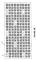
- pixel sensors 10 of pixel sensor array 180 are read in a skewed sub-sampling mode whereby the non-shaded sensors are read and the shaded sensors are not.
- the top row and every-other-row from the top row form a set of "G-R" rows.
- Half of the G-R rows have a read sub-set of a G and an adjacent R sensor (forming the top half of a Bayer pattern).
- the other half of the G-R rows do not have any sensors to be read.
- each G-R series of sensors to be read forms a read sub-set which is separated from another G-R series of sensors to be read by three G-R series sets of sensors which will not be read (in this skewed sub-sampling mode).
- each B-G series of sensors to be read forms a read sub-set which is separated from another B-G series of sensors to be read by three B-G series sets of sensors which will not be read (in this skewed sub-sampling mode).
- the skewing of the sub-sampling pattern shown in Figure 5B is such that for a pair of adjoining rows, a pixel in G-R read sub-set will not have a pixel in a B-G read subset in the same column.
- the G sensor in the left-most column of the top row will be read, but none of the B sensors beneath it in the left-most column will be read.
- whole columns of sensors are not read in Figure 5B because of the higher sub-sampling rate.
- whole rows of sensors are also not read because of the higher sub-sampling rate.
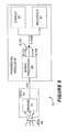
- FIG. 6 shows schematically the layout of a solid state camera system 70 incorporating the image array sensor of Figure 1 (referenced as 12 in Figure 6).
- the camera system includes a camera head 50 comprising a lens 54 and the image array sensor 12.
- the signal stream of pixel outputs read out at the main array output are fed to an analog to digital convertor where the pixel outputs are converted from analog to digital signals.
- the digital signals 170 are subsequently fed to a signal processing unit 68 which may be configured and/or programmed to demultiplex the pixel output streams into red, green and blue color channels (R-CH, G-CH, B-CH) of a video signal V-RGB.
- R-CH, G-CH, B-CH red, green and blue color channels
- Video signal V-RGB is output by the processing unit 68 to a video display unit 60, and/or a recording device 62, coupled to the processing unit 68.
- the processing unit preferably also interpolates the red, green and blue channel signals to form synchronous, parallel color channel signals for the video signal V-RGB before being output to the display unit 60, and/or recording device 64.
- the processing unit 68 is provided on a second integrated circuit which is provided together with the display unit 60 and/or recording device 64 in an image processing unit or module 66 of the camera system 70 for use with the camera head 50.
- the A/D convertor is provided in circuitry incorporated in the camera head 22, (which could, if desired, be integrally provided in the image sensor integrated circuit).
- the second integrated circuit may also include demosaicing, color balance control circuitry and/or exposure control circuitry of the camera system.
- the camera head 50 need not always be used with the image processing unit 68 shown in the camera system of Figure 6. It would be possible, for example, for image data output from the image sensor 12 in the camera head 50 to be fed straight to a recording device where the output signal streams would be recorded on a recording medium (e.g. a computer hard disk, or a floppy disk).
- a recording medium e.g. a computer hard disk, or a floppy disk.
- the recorded image data in its output signal stream form
- the A/D convertor is incorporated in the image processing unit 68, rather than in the camera head.
- A/D conversion and some, or all, of the signal processing performed by the processing unit 68 is carried out in the camera head 50. This may be done, for example, by processing circuitry included on the same chip as that on which the integrated circuit image array sensor is formed.
- the processing circuitry on the chip may thus be configured to digitally format the image data output from the sensor and to convert the formatted data into a standard video form which can be input directly to a video display unit and/or recorder device, or stored in an external memory for future use.
- the processing circuitry on the chip may be configured to convert the image data output from the sensor into a particular digital format, the formatted data then being output from the camera head 50 to further external signal processing circuitry which is programmed, or configured, to interpret the formatted data and produce therefrom a standard video signal (e.g. in three channel R, G, B form) for use as before.
- a standard video signal e.g. in three channel R, G, B form
- the invention is suitable for multispectral sensors in which some of the pixels are treated so as to sense non-visible radiation which may, for example, be infra-red radiation.
- non-visible radiation may, for example, be infra-red radiation.
- at least one of said plurality of channels may be for infra-red or other non-visible radiation and some of the sensing cells may consequently be for sensing infra-red or other non-visible radiation respectively.
- the array of sensing cells has been shown to include a matrixed pattern of filters corresponding to different radiation wavelengths so as to enable essentially similar sensing cells to sense radiation at a particular wavelength, or over a particular band of wavelengths, corresponding to a respective one of said plurality of channels.
- filters corresponding to different radiation wavelengths so as to enable essentially similar sensing cells to sense radiation at a particular wavelength, or over a particular band of wavelengths, corresponding to a respective one of said plurality of channels.
Landscapes
- Engineering & Computer Science (AREA)
- Multimedia (AREA)
- Signal Processing (AREA)
- Physics & Mathematics (AREA)
- Spectroscopy & Molecular Physics (AREA)
- Color Television Image Signal Generators (AREA)
Applications Claiming Priority (2)
| Application Number | Priority Date | Filing Date | Title |
|---|---|---|---|
| US62429700A | 2000-07-24 | 2000-07-24 | |
| US624297 | 2000-07-24 |
Publications (1)
| Publication Number | Publication Date |
|---|---|
| EP1176807A1 true EP1176807A1 (de) | 2002-01-30 |
Family
ID=24501434
Family Applications (1)
| Application Number | Title | Priority Date | Filing Date |
|---|---|---|---|
| EP01109924A Withdrawn EP1176807A1 (de) | 2000-07-24 | 2001-04-24 | Unterabtastung von Bildsensoren mit geneigtem Farbfiltermuster |
Country Status (3)
| Country | Link |
|---|---|
| EP (1) | EP1176807A1 (de) |
| KR (1) | KR20020009457A (de) |
| CN (1) | CN1342020A (de) |
Cited By (7)
| Publication number | Priority date | Publication date | Assignee | Title |
|---|---|---|---|---|
| WO2007126288A1 (en) * | 2006-05-01 | 2007-11-08 | Pixelplus Co., Ltd. | Wide dynamic range image sensor |
| WO2009108182A1 (en) * | 2008-02-25 | 2009-09-03 | Sorin Davidovici | System and method for a high dynamic range image sensor sensitive array |
| US9237276B2 (en) | 2008-12-22 | 2016-01-12 | Thomson Licensing | Method and device to capture images by emulating a mechanical shutter |
| US9423602B1 (en) * | 2009-12-31 | 2016-08-23 | Gene Dolgoff | Practical stereoscopic 3-D television display system |
| EP3275177A4 (de) * | 2015-07-09 | 2018-04-18 | Huawei Technologies Co., Ltd. | Bildgebungsverfahren, bildsensor und bildgebungsvorrichtung |
| EP4395297A4 (de) * | 2021-08-25 | 2024-11-27 | Vivo Mobile Communication Co., Ltd. | Bildsensor, steuerungsverfahren, steuerungsvorrichtung, elektronische vorrichtung und speichermedium |
| EP4598043A3 (de) * | 2024-02-02 | 2025-09-10 | Varjo Technologies Oy | Simultane unterabtastung und bildgebung mit hohem dynamikbereich in farbfilterarrays |
Families Citing this family (10)
| Publication number | Priority date | Publication date | Assignee | Title |
|---|---|---|---|---|
| US6783900B2 (en) * | 2002-05-13 | 2004-08-31 | Micron Technology, Inc. | Color filter imaging array and method of formation |
| KR100460774B1 (ko) * | 2002-10-10 | 2004-12-09 | 매그나칩 반도체 유한회사 | 어드레스 서브샘플링 장치 및 그 방법과 이미지센서 및이미지센서의 어드레스 서브샘플링 방법 |
| KR100588731B1 (ko) * | 2004-04-26 | 2006-06-12 | 매그나칩 반도체 유한회사 | 고속 아날로그 신호 처리를 위한 cmos 이미지센서 |
| KR100686930B1 (ko) * | 2004-06-08 | 2007-02-27 | 엠텍비젼 주식회사 | Cmos 이미지 센서 |
| KR20050118510A (ko) * | 2004-06-14 | 2005-12-19 | 엘지전자 주식회사 | 디스플레이기기의 해상도 향상 장치 및 그 구동방법 |
| CN100531350C (zh) * | 2005-05-20 | 2009-08-19 | 凌阳科技股份有限公司 | 储存影像资料的方法与装置 |
| JP2006345209A (ja) * | 2005-06-08 | 2006-12-21 | Sony Corp | 入力装置、情報処理装置、情報処理方法、及びプログラム |
| KR101643773B1 (ko) * | 2009-12-03 | 2016-07-28 | 삼성전자주식회사 | 프리뷰 영상의 화질을 개선하기 위한 장치 및 방법 |
| KR102003815B1 (ko) * | 2012-03-23 | 2019-10-01 | 에스케이하이닉스 주식회사 | 이미지 센서 및 그 동작 방법 |
| US9204143B2 (en) | 2013-03-15 | 2015-12-01 | Samsung Electronics Co., Ltd. | Image sensor, operation method thereof, and system including the same |
Citations (1)
| Publication number | Priority date | Publication date | Assignee | Title |
|---|---|---|---|---|
| EP0920215A1 (de) * | 1997-06-16 | 1999-06-02 | Sony Corporation | Bildverarbeitungsvorrichtung und -verfahren, übertragungsmedium und -verfahren sowie bildformat |
-
2001
- 2001-04-24 EP EP01109924A patent/EP1176807A1/de not_active Withdrawn
- 2001-07-23 KR KR1020010044098A patent/KR20020009457A/ko not_active Withdrawn
- 2001-07-24 CN CN01123091A patent/CN1342020A/zh active Pending
Patent Citations (1)
| Publication number | Priority date | Publication date | Assignee | Title |
|---|---|---|---|---|
| EP0920215A1 (de) * | 1997-06-16 | 1999-06-02 | Sony Corporation | Bildverarbeitungsvorrichtung und -verfahren, übertragungsmedium und -verfahren sowie bildformat |
Cited By (11)
| Publication number | Priority date | Publication date | Assignee | Title |
|---|---|---|---|---|
| WO2007126288A1 (en) * | 2006-05-01 | 2007-11-08 | Pixelplus Co., Ltd. | Wide dynamic range image sensor |
| WO2009108182A1 (en) * | 2008-02-25 | 2009-09-03 | Sorin Davidovici | System and method for a high dynamic range image sensor sensitive array |
| US9237276B2 (en) | 2008-12-22 | 2016-01-12 | Thomson Licensing | Method and device to capture images by emulating a mechanical shutter |
| US9423602B1 (en) * | 2009-12-31 | 2016-08-23 | Gene Dolgoff | Practical stereoscopic 3-D television display system |
| US10298904B1 (en) | 2009-12-31 | 2019-05-21 | Gene Dolgoff | Practical stereoscopic 3-D television system |
| EP3275177A4 (de) * | 2015-07-09 | 2018-04-18 | Huawei Technologies Co., Ltd. | Bildgebungsverfahren, bildsensor und bildgebungsvorrichtung |
| US10491837B2 (en) | 2015-07-09 | 2019-11-26 | Huawei Technologies Co., Ltd. | Imaging method, image sensor, and imaging device |
| EP4395297A4 (de) * | 2021-08-25 | 2024-11-27 | Vivo Mobile Communication Co., Ltd. | Bildsensor, steuerungsverfahren, steuerungsvorrichtung, elektronische vorrichtung und speichermedium |
| US12610149B2 (en) | 2021-08-25 | 2026-04-21 | Vivo Mobile Communication Co., Ltd. | Image sensor, control method, control apparatus, electronic device, and storage medium |
| EP4598043A3 (de) * | 2024-02-02 | 2025-09-10 | Varjo Technologies Oy | Simultane unterabtastung und bildgebung mit hohem dynamikbereich in farbfilterarrays |
| US12627904B2 (en) | 2024-02-02 | 2026-05-12 | Varjo Technologies Oy | Simultaneous subsampling and high dynamic range imaging in colour filter arrays |
Also Published As
| Publication number | Publication date |
|---|---|
| CN1342020A (zh) | 2002-03-27 |
| KR20020009457A (ko) | 2002-02-01 |
Similar Documents
| Publication | Publication Date | Title |
|---|---|---|
| US20240006427A1 (en) | Imaging device and imaging system | |
| US10868971B2 (en) | System and method for visible and infrared high dynamic range sensing | |
| EP2323409B1 (de) | Bildsensor mit Ladungs-binning | |
| EP1530873B1 (de) | Farbkamera mit einem chip für niedrige lichtpegel | |
| JP4500574B2 (ja) | 広ダイナミックレンジカラー固体撮像装置及びこの固体撮像装置を搭載したデジタルカメラ | |
| US8902330B2 (en) | Method for correcting image data from an image sensor having image pixels and non-image pixels, and image sensor implementing same | |
| US20100149393A1 (en) | Increasing the resolution of color sub-pixel arrays | |
| US7768569B2 (en) | High sensitivity color filter array | |
| US20070090274A1 (en) | Image sensors including active pixel sensor arrays | |
| JP4448889B2 (ja) | 撮像素子及び撮像装置 | |
| KR20020009457A (ko) | 촬상 장치 및 촬상 방법 | |
| US8471941B2 (en) | Missing pixel array | |
| JP4423452B2 (ja) | 固体撮像装置 | |
| US7893981B2 (en) | Image sensor with variable resolution and sensitivity | |
| US7379107B2 (en) | Image sensor for still or video photography | |
| JP3950655B2 (ja) | 撮像装置 | |
| US20050104989A1 (en) | Dual-type solid state color image pickup apparatus and digital camera | |
| US7655892B2 (en) | Solid-state imaging device, and method of driving solid-state imaging device | |
| US7061655B2 (en) | Provision of bright and high quality image from CCD image pick-up device | |
| US7643079B2 (en) | Control circuit for reading out signal charges from main and subsidiary pixels of a solid-state image sensor separately from each other in interlace scanning | |
| JP4848349B2 (ja) | 撮像装置及び固体撮像素子の駆動方法 | |
| CN101010938A (zh) | 用于静态或视频摄影的图像传感器 | |
| JP2007088733A (ja) | Ccd型単板式カラー固体撮像素子 | |
| JP2004146955A (ja) | 固体撮像素子及びその駆動方法 |
Legal Events
| Date | Code | Title | Description |
|---|---|---|---|
| PUAI | Public reference made under article 153(3) epc to a published international application that has entered the european phase |
Free format text: ORIGINAL CODE: 0009012 |
|
| AK | Designated contracting states |
Kind code of ref document: A1 Designated state(s): DE ES FR GB Kind code of ref document: A1 Designated state(s): AT BE CH CY DE DK ES FI FR GB GR IE IT LI LU MC NL PT SE TR |
|
| AX | Request for extension of the european patent |
Free format text: AL;LT;LV;MK;RO;SI |
|
| 17P | Request for examination filed |
Effective date: 20020326 |
|
| AKX | Designation fees paid |
Free format text: DE ES FR GB |
|
| STAA | Information on the status of an ep patent application or granted ep patent |
Free format text: STATUS: THE APPLICATION HAS BEEN WITHDRAWN |
|
| 18W | Application withdrawn |
Effective date: 20040205 |