EP1178512A2 - Flache Plasma-Anzeigetafel mit gesteuerten Plasma-Aufrechterhaltungselektroden - Google Patents
Flache Plasma-Anzeigetafel mit gesteuerten Plasma-Aufrechterhaltungselektroden Download PDFInfo
- Publication number
- EP1178512A2 EP1178512A2 EP01118278A EP01118278A EP1178512A2 EP 1178512 A2 EP1178512 A2 EP 1178512A2 EP 01118278 A EP01118278 A EP 01118278A EP 01118278 A EP01118278 A EP 01118278A EP 1178512 A2 EP1178512 A2 EP 1178512A2
- Authority
- EP
- European Patent Office
- Prior art keywords
- sustainer
- electrodes
- electrode
- substrate
- auxiliary
- Prior art date
- Legal status (The legal status is an assumption and is not a legal conclusion. Google has not performed a legal analysis and makes no representation as to the accuracy of the status listed.)
- Withdrawn
Links
- 239000000758 substrate Substances 0.000 claims abstract description 115
- OAICVXFJPJFONN-UHFFFAOYSA-N Phosphorus Chemical compound [P] OAICVXFJPJFONN-UHFFFAOYSA-N 0.000 claims abstract description 19
- 239000000463 material Substances 0.000 claims description 19
- 238000000034 method Methods 0.000 claims description 19
- 239000003989 dielectric material Substances 0.000 claims description 9
- 230000000977 initiatory effect Effects 0.000 claims description 9
- 239000011800 void material Substances 0.000 claims description 9
- 238000005286 illumination Methods 0.000 claims description 5
- 239000011521 glass Substances 0.000 abstract description 16
- 230000004888 barrier function Effects 0.000 abstract description 13
- 239000007789 gas Substances 0.000 description 15
- 229910052737 gold Inorganic materials 0.000 description 6
- 229910052804 chromium Inorganic materials 0.000 description 5
- 239000010408 film Substances 0.000 description 5
- 229910052802 copper Inorganic materials 0.000 description 4
- 238000004519 manufacturing process Methods 0.000 description 4
- 239000000203 mixture Substances 0.000 description 4
- 239000011159 matrix material Substances 0.000 description 3
- 238000003860 storage Methods 0.000 description 3
- VYPSYNLAJGMNEJ-UHFFFAOYSA-N Silicium dioxide Chemical compound O=[Si]=O VYPSYNLAJGMNEJ-UHFFFAOYSA-N 0.000 description 2
- 238000003491 array Methods 0.000 description 2
- 238000000151 deposition Methods 0.000 description 2
- 230000008021 deposition Effects 0.000 description 2
- 238000010586 diagram Methods 0.000 description 2
- 229910052754 neon Inorganic materials 0.000 description 2
- GKAOGPIIYCISHV-UHFFFAOYSA-N neon atom Chemical compound [Ne] GKAOGPIIYCISHV-UHFFFAOYSA-N 0.000 description 2
- 229910052709 silver Inorganic materials 0.000 description 2
- 230000002459 sustained effect Effects 0.000 description 2
- 229910052724 xenon Inorganic materials 0.000 description 2
- FHNFHKCVQCLJFQ-UHFFFAOYSA-N xenon atom Chemical compound [Xe] FHNFHKCVQCLJFQ-UHFFFAOYSA-N 0.000 description 2
- KKCBUQHMOMHUOY-UHFFFAOYSA-N Na2O Inorganic materials [O-2].[Na+].[Na+] KKCBUQHMOMHUOY-UHFFFAOYSA-N 0.000 description 1
- PNEYBMLMFCGWSK-UHFFFAOYSA-N aluminium oxide Inorganic materials [O-2].[O-2].[O-2].[Al+3].[Al+3] PNEYBMLMFCGWSK-UHFFFAOYSA-N 0.000 description 1
- 239000003990 capacitor Substances 0.000 description 1
- 239000011248 coating agent Substances 0.000 description 1
- 238000000576 coating method Methods 0.000 description 1
- 229910052681 coesite Inorganic materials 0.000 description 1
- 239000002131 composite material Substances 0.000 description 1
- 239000004020 conductor Substances 0.000 description 1
- 229910052593 corundum Inorganic materials 0.000 description 1
- 229910052906 cristobalite Inorganic materials 0.000 description 1
- 229910003460 diamond Inorganic materials 0.000 description 1
- 239000010432 diamond Substances 0.000 description 1
- 238000001962 electrophoresis Methods 0.000 description 1
- 238000010304 firing Methods 0.000 description 1
- 239000002241 glass-ceramic Substances 0.000 description 1
- 229910052734 helium Inorganic materials 0.000 description 1
- 239000001307 helium Substances 0.000 description 1
- SWQJXJOGLNCZEY-UHFFFAOYSA-N helium atom Chemical compound [He] SWQJXJOGLNCZEY-UHFFFAOYSA-N 0.000 description 1
- AMGQUBHHOARCQH-UHFFFAOYSA-N indium;oxotin Chemical compound [In].[Sn]=O AMGQUBHHOARCQH-UHFFFAOYSA-N 0.000 description 1
- 239000004615 ingredient Substances 0.000 description 1
- 150000002500 ions Chemical class 0.000 description 1
- 239000005355 lead glass Substances 0.000 description 1
- 239000002075 main ingredient Substances 0.000 description 1
- 229910052751 metal Inorganic materials 0.000 description 1
- 239000002184 metal Substances 0.000 description 1
- 238000001465 metallisation Methods 0.000 description 1
- 150000002739 metals Chemical class 0.000 description 1
- 239000002667 nucleating agent Substances 0.000 description 1
- 230000035515 penetration Effects 0.000 description 1
- 230000005855 radiation Effects 0.000 description 1
- 229910052706 scandium Inorganic materials 0.000 description 1
- 239000000377 silicon dioxide Substances 0.000 description 1
- 125000006850 spacer group Chemical group 0.000 description 1
- 229910052682 stishovite Inorganic materials 0.000 description 1
- 239000013589 supplement Substances 0.000 description 1
- 239000010409 thin film Substances 0.000 description 1
- 238000000427 thin-film deposition Methods 0.000 description 1
- 229910052905 tridymite Inorganic materials 0.000 description 1
- 230000000007 visual effect Effects 0.000 description 1
- 229910001845 yogo sapphire Inorganic materials 0.000 description 1
Images


Classifications
-
- H—ELECTRICITY
- H01—ELECTRIC ELEMENTS
- H01J—ELECTRIC DISCHARGE TUBES OR DISCHARGE LAMPS
- H01J11/00—Gas-filled discharge tubes with alternating current induction of the discharge, e.g. alternating current plasma display panels [AC-PDP]; Gas-filled discharge tubes without any main electrode inside the vessel; Gas-filled discharge tubes with at least one main electrode outside the vessel
- H01J11/20—Constructional details
- H01J11/22—Electrodes, e.g. special shape, material or configuration
- H01J11/28—Auxiliary electrodes, e.g. priming electrodes or trigger electrodes
-
- H—ELECTRICITY
- H01—ELECTRIC ELEMENTS
- H01J—ELECTRIC DISCHARGE TUBES OR DISCHARGE LAMPS
- H01J11/00—Gas-filled discharge tubes with alternating current induction of the discharge, e.g. alternating current plasma display panels [AC-PDP]; Gas-filled discharge tubes without any main electrode inside the vessel; Gas-filled discharge tubes with at least one main electrode outside the vessel
- H01J11/10—AC-PDPs with at least one main electrode being out of contact with the plasma
- H01J11/12—AC-PDPs with at least one main electrode being out of contact with the plasma with main electrodes provided on both sides of the discharge space
-
- H—ELECTRICITY
- H01—ELECTRIC ELEMENTS
- H01J—ELECTRIC DISCHARGE TUBES OR DISCHARGE LAMPS
- H01J11/00—Gas-filled discharge tubes with alternating current induction of the discharge, e.g. alternating current plasma display panels [AC-PDP]; Gas-filled discharge tubes without any main electrode inside the vessel; Gas-filled discharge tubes with at least one main electrode outside the vessel
- H01J11/20—Constructional details
- H01J11/22—Electrodes, e.g. special shape, material or configuration
- H01J11/24—Sustain electrodes or scan electrodes
-
- H—ELECTRICITY
- H01—ELECTRIC ELEMENTS
- H01J—ELECTRIC DISCHARGE TUBES OR DISCHARGE LAMPS
- H01J11/00—Gas-filled discharge tubes with alternating current induction of the discharge, e.g. alternating current plasma display panels [AC-PDP]; Gas-filled discharge tubes without any main electrode inside the vessel; Gas-filled discharge tubes with at least one main electrode outside the vessel
- H01J11/20—Constructional details
- H01J11/22—Electrodes, e.g. special shape, material or configuration
- H01J11/26—Address electrodes
-
- G—PHYSICS
- G09—EDUCATION; CRYPTOGRAPHY; DISPLAY; ADVERTISING; SEALS
- G09G—ARRANGEMENTS OR CIRCUITS FOR CONTROL OF INDICATING DEVICES USING STATIC MEANS TO PRESENT VARIABLE INFORMATION
- G09G2310/00—Command of the display device
- G09G2310/02—Addressing, scanning or driving the display screen or processing steps related thereto
- G09G2310/0202—Addressing of scan or signal lines
- G09G2310/0218—Addressing of scan or signal lines with collection of electrodes in groups for n-dimensional addressing
-
- G—PHYSICS
- G09—EDUCATION; CRYPTOGRAPHY; DISPLAY; ADVERTISING; SEALS
- G09G—ARRANGEMENTS OR CIRCUITS FOR CONTROL OF INDICATING DEVICES USING STATIC MEANS TO PRESENT VARIABLE INFORMATION
- G09G3/00—Control arrangements or circuits, of interest only in connection with visual indicators other than cathode-ray tubes
- G09G3/20—Control arrangements or circuits, of interest only in connection with visual indicators other than cathode-ray tubes for presentation of an assembly of a number of characters, e.g. a page, by composing the assembly by combination of individual elements arranged in a matrix no fixed position being assigned to or needed to be assigned to the individual characters or partial characters
- G09G3/22—Control arrangements or circuits, of interest only in connection with visual indicators other than cathode-ray tubes for presentation of an assembly of a number of characters, e.g. a page, by composing the assembly by combination of individual elements arranged in a matrix no fixed position being assigned to or needed to be assigned to the individual characters or partial characters using controlled light sources
- G09G3/28—Control arrangements or circuits, of interest only in connection with visual indicators other than cathode-ray tubes for presentation of an assembly of a number of characters, e.g. a page, by composing the assembly by combination of individual elements arranged in a matrix no fixed position being assigned to or needed to be assigned to the individual characters or partial characters using controlled light sources using luminous gas-discharge panels, e.g. plasma panels
- G09G3/288—Control arrangements or circuits, of interest only in connection with visual indicators other than cathode-ray tubes for presentation of an assembly of a number of characters, e.g. a page, by composing the assembly by combination of individual elements arranged in a matrix no fixed position being assigned to or needed to be assigned to the individual characters or partial characters using controlled light sources using luminous gas-discharge panels, e.g. plasma panels using AC panels
- G09G3/291—Control arrangements or circuits, of interest only in connection with visual indicators other than cathode-ray tubes for presentation of an assembly of a number of characters, e.g. a page, by composing the assembly by combination of individual elements arranged in a matrix no fixed position being assigned to or needed to be assigned to the individual characters or partial characters using controlled light sources using luminous gas-discharge panels, e.g. plasma panels using AC panels controlling the gas discharge to control a cell condition, e.g. by means of specific pulse shapes
- G09G3/292—Control arrangements or circuits, of interest only in connection with visual indicators other than cathode-ray tubes for presentation of an assembly of a number of characters, e.g. a page, by composing the assembly by combination of individual elements arranged in a matrix no fixed position being assigned to or needed to be assigned to the individual characters or partial characters using controlled light sources using luminous gas-discharge panels, e.g. plasma panels using AC panels controlling the gas discharge to control a cell condition, e.g. by means of specific pulse shapes for reset discharge, priming discharge or erase discharge occurring in a phase other than addressing
- G09G3/2927—Details of initialising
-
- G—PHYSICS
- G09—EDUCATION; CRYPTOGRAPHY; DISPLAY; ADVERTISING; SEALS
- G09G—ARRANGEMENTS OR CIRCUITS FOR CONTROL OF INDICATING DEVICES USING STATIC MEANS TO PRESENT VARIABLE INFORMATION
- G09G3/00—Control arrangements or circuits, of interest only in connection with visual indicators other than cathode-ray tubes
- G09G3/20—Control arrangements or circuits, of interest only in connection with visual indicators other than cathode-ray tubes for presentation of an assembly of a number of characters, e.g. a page, by composing the assembly by combination of individual elements arranged in a matrix no fixed position being assigned to or needed to be assigned to the individual characters or partial characters
- G09G3/22—Control arrangements or circuits, of interest only in connection with visual indicators other than cathode-ray tubes for presentation of an assembly of a number of characters, e.g. a page, by composing the assembly by combination of individual elements arranged in a matrix no fixed position being assigned to or needed to be assigned to the individual characters or partial characters using controlled light sources
- G09G3/28—Control arrangements or circuits, of interest only in connection with visual indicators other than cathode-ray tubes for presentation of an assembly of a number of characters, e.g. a page, by composing the assembly by combination of individual elements arranged in a matrix no fixed position being assigned to or needed to be assigned to the individual characters or partial characters using controlled light sources using luminous gas-discharge panels, e.g. plasma panels
- G09G3/288—Control arrangements or circuits, of interest only in connection with visual indicators other than cathode-ray tubes for presentation of an assembly of a number of characters, e.g. a page, by composing the assembly by combination of individual elements arranged in a matrix no fixed position being assigned to or needed to be assigned to the individual characters or partial characters using controlled light sources using luminous gas-discharge panels, e.g. plasma panels using AC panels
- G09G3/298—Control arrangements or circuits, of interest only in connection with visual indicators other than cathode-ray tubes for presentation of an assembly of a number of characters, e.g. a page, by composing the assembly by combination of individual elements arranged in a matrix no fixed position being assigned to or needed to be assigned to the individual characters or partial characters using controlled light sources using luminous gas-discharge panels, e.g. plasma panels using AC panels using surface discharge panels
- G09G3/2983—Control arrangements or circuits, of interest only in connection with visual indicators other than cathode-ray tubes for presentation of an assembly of a number of characters, e.g. a page, by composing the assembly by combination of individual elements arranged in a matrix no fixed position being assigned to or needed to be assigned to the individual characters or partial characters using controlled light sources using luminous gas-discharge panels, e.g. plasma panels using AC panels using surface discharge panels using non-standard pixel electrode arrangements
-
- H—ELECTRICITY
- H01—ELECTRIC ELEMENTS
- H01J—ELECTRIC DISCHARGE TUBES OR DISCHARGE LAMPS
- H01J2211/00—Plasma display panels with alternate current induction of the discharge, e.g. AC-PDPs
- H01J2211/20—Constructional details
- H01J2211/46—Connecting or feeding means, e.g. leading-in conductors
Definitions
- This invention relates in general to a flat plasma display panel and in particular to an improved structure for a full color, high resolution capable flat plasma display panel which operates at a high efficiency and includes independent trigger and controlled sustaining electrodes.
- a flat plasma display panel is an electronic display in which a large orthogonal array of display pixels, such as electro-luminescent devices, AC plasma display panels, DC plasma display panels and field emission displays and the like form a flat screen.
- the basic structure of an AC Plasma Display Panel, or PDP comprises two glass plates with a conductor pattern of electrodes on the inner surfaces of each plate.
- the plates are separated by a gas filled gap.
- the electrodes are configured in an x-y matrix with the electrodes on each plate deposited at right angles to each other using conventional thin or thick film techniques.
- At least one set of sustaining electrodes of the AC PDP is covered with a thin glass dielectric layer.
- the glass plates are assembled into a sandwich with the gap between the plates fixed by spacers. The edges of the plates are sealed and the cavity between the plates is evacuated and filled with a mixture of neon and xenon gases or a similar gas mixture of a type well known in the art.
- a sufficient driver voltage pulse is applied to the electrodes to ionize the gas contained between the plates.
- the dielectrics charge like small capacitors, which reduces the voltage across the gas and extinguishes the discharge.
- the capacitive voltages are due to stored charge and are conventionally called wall charge.
- the voltage is then reversed, and the sum of the driver voltage and wall charge voltages is again large enough to excite the gas and produce a glow discharge pulse.
- a sequence of such driver voltages repetitively applied is called the sustaining voltage, or sustainer.
- sustainer waveform pixels which have had charge stored will discharge and emit light pulses at every sustainer cycle. Pixels which have no charge stored will not emit light.
- appropriate waveforms are applied across the x-y matrix of electrodes, small light emitting pixels form a visual picture.
- barrier ribs are typically disposed between the plates to prevent cross-color and cross-pixel interference between the electrodes.
- the barrier ribs also increase the resolution to provide a sharply defined picture.
- the barrier ribs further provide a uniform discharge space between the glass plates by utilizing the barrier rib height, width and pattern gap to achieve a desired pixel pitch.
- This invention relates to an improved plasma flat plasma display panel which operates at a high efficiency and includes independent trigger and controlled sustaining electrodes.
- plasma flat plasma display panels having pairs of sustaining electrodes which establish a charged volume between the display substrates.
- the charge supports a plasma discharge that is controlled by applying voltages to a plurality of address electrodes.
- the charged volume is established by applying an initial voltage to the sustaining electrodes.
- the actual plasma discharge is initiated between the sustaining electrodes by applying a second sustaining voltage to the sustaining electrodes.
- the efficiency of the panel is generally greater when gas and geometry parameters are adjusted to increase the voltage required to sustain a discharge.
- this causes complexity for the associated voltage supply circuits with respect to the initiating voltage. Therefore, it would be desirable to develop a plasma display panel that would allow initiation and control of the sustaining discharge with a relatively low voltage while sustaining the resulting plasma discharge with a relatively high voltage.
- each of the electrodes in a plasma display panel with a separate voltage driver.
- the total number of voltage drivers and their physical connections to the panel electrodes add considerable bulk and cost to the final display panel. Accordingly, it also would be desirable to reduce the number of separate voltage drivers.
- the present invention contemplates a plasma flat-panel display having a first transparent substrate with a first pair of parallel sustainer electrodes deposited upon thereon.
- the first pair of sustainer electrodes include a first sustainer electrode and a second sustainer electrode.
- the display also includes at least one auxiliary electrode deposited upon the first substrate parallel to the first pair of sustainer electrodes and adjacent to the first sustainer electrode in the first pair of sustainer electrodes.
- a second pair of parallel sustainer electrodes is deposited upon the first substrate parallel to the auxiliary electrode, the second pair of sustainer electrodes including a first sustainer electrode and a second sustainer electrode.
- the second sustainer electrode pair is oriented upon the first substrate as a mirror image of the first sustainer electrode pair with the first sustainer electrode in the second pair of sustainer electrodes adjacent to the auxiliary electrode.
- a single common first sustainer electrode pad is electrically connected to the first sustainer electrode in the first sustainer electrode pair and the first sustainer electrode in the second sustainer electrode pair.
- the first sustainer electrode pad is adapted be to connected to a first sustainer voltage waveform supply so that a single supply provides a first sustainer voltage waveform to both of the first sustainer electrodes.
- a layer of dielectric material covers the sustainer and auxiliary electrodes.
- a protection layer is formed covering the dielectric layer.
- the display further includes a second substrate which is hermetically sealed to the first substrate with the second substrate having a plurality of micro-voids formed in a surface thereof that is adjacent to the first substrate.
- the micro-voids are filled with a gas and cooperate with the first substrate to define a plurality of sub-pixels.
- a phosphor material is deposited within each micro-void and a plurality of address electrodes are incorporated within said second substrate. Each of the address electrodes correspond to one of the sub-pixels.
- the present invention also contemplates a method for operating a plasma flat-panel display that includes applying in a set-up period first and second sustain, auxiliary, and address voltage waveforms to corresponding electrodes. Similar electrodes are connected by pads to cause the setting of all wall charge on associated dielectric surfaces corresponding to the controlled discharge volumes of sub-cells to values appropriate to an "off" state. A first auxiliary voltage waveform is then applied in an addressing period in conjunction with an address voltage waveform sequentially for each auxiliary voltage waveform supply connected by pads to corresponding first auxiliary electrodes.
- the first auxiliary voltage waveform selectively initiates discharges between associated first and second sustain electrode pairs, thereby setting the wall charge on the dielectric surfaces associated with the sustainer electrodes corresponding to the controlled discharge volumes of selected sub-cells to values appropriate to an "on" state. Subsequently, a pre-determined number of voltage pulses via first and second sustain waveform supplies are applied during a sustaining period to create a pre-determined number of discharges in a sequence corresponding to the voltage pulses in cells set to an "on" state with the discharges controlled in position and shape by auxiliary voltage waveform supplies.
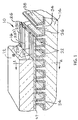
- a plasma display panel 10 which, in the preferred embodiment, is an AC PDP.
- PDP plasma display panel
- like reference characters designate like or corresponding parts.
- top, bottom, forward, “rearward”, and similar terms of position and direction are used in reference to the drawings and for convenience in description.
- the PDP 10 comprises a hermetically sealed gas filled enclosure including a top glass substrate 12 and a spaced apart bottom glass substrate 14.
- the top glass substrate 12 is superposed upon the bottom glass substrate 14.
- the glass substrates 12 and 14 are typically both transmissive to light and of a uniform thickness, although only the viewing side, normally the top substrate 12, is required to be transparent to visible light.
- the glass substrates 12 and 14 may be approximately 1/8 to 1/4 inch thick.
- the top glass substrate 12 may contain SiO 2 , Al 2 O 3 , MgO 2 and CaO as the main ingredients and Na 2 O, K 2 O, PbO, B 2 O 3 and the like as accessory ingredients.
- Deposited upon a lower surface 16 of the top substrate 12 are a plurality of sets of parallel electrodes.
- One such set, which is labeled 18, is illustrated in Fig. 1.
- Each set of electrodes includes an inner pair of display, or sustainer, electrodes 22 and 23, which typically have a spacing of approximately 800 microns.
- the sustainer electrode 22 that is in the foreground in Fig.
- first sustainer electrode and also labeled Y Disposed adjacent and parallel to the first sustainer electrode 22 is a trigger electrode 24 that also is labeled T in the following.
- a control electrode 25, that is also labeled C in the following is disposed adjacent and parallel to the second sustainer electrode 23.
- the sustainer electrodes 22 and 23 are between the trigger electrode 24 and the control electrode 25.
- the trigger and control electrodes 24 and 25 typically have a spacing from the corresponding sustainer electrode, 22 and 23, within the range of 100 microns to 400 microns.
- the electrodes 22, 23, 24 and 25 are formed by a conventional process.
- the electrodes 22, 23, 24 and 25 are thin film electrodes prepared from evaporated metals such as Au, Cr and Au, Cu and Au, Cu and Cr, ITO and Au, Ag, or Cr and the like.
- a uniform charge storage film 26 such as a dielectric film of a type well known in the art covers the electrodes 22, 23, 24 and 25 by a variety of planar techniques well known in the art of display manufacture.
- the charge storage film 26 may be of most any suitable material, such as a lead glass material.
- the charge storage film 26 is covered by a thin electron emissive layer 27
- the electron emissive layer 27 may be formed from most any suitable material, such as diamond overcoating, MgO, or the like. As will be explained below, the electron emissive layer 27 may be uniform or patterned.
- a plurality of parallel microgrooves 32 are formed into the upper surface of the bottom substrate 14.
- the microgrooves 32 are generally perpendicular to the electrodes 22, 23, 24 and 25 deposited upon the top substrate 12.
- the microgrooves 32 are separated by barrier ribs 34 which extend in an upward direction in Fig. 1.
- the upper end of each of the barrier ribs 34 contacts the electron emissive layer 27 that is deposited upon the lower surface 16 of the top substrate 12.
- the microgrooves 32 and barrier ribs 34 can be formed into an intermediate glass layer which is disposed between the top and bottom substrates 12 and 14. (not shown).
- the microgrooves 32 and barrier ribs 34 are preferably formed from an etchable glass material which is inherently selectively crystallizing, such as, a glass-ceramic composite doped with suitable nucleating agents.
- Address electrodes 36 that are also labeled X in the following are deposited within each microgroove 32.
- the address electrodes 36 are deposited along the base and surrounding sidewalls of the microgrooves 32 to increase uniformity of firing and provide optimum phosphor coating along the entire surface of the microgroove 32.
- the address electrodes 36 are deposited by selectively metalizing a thin layer of Cr and Au or Cu and Au, or Indium Tin Oxide (ITO) and Au, or Cu and Cr, or Ag or Cr within the microgroove surfaces.
- the metalization may be accomplished by thin film deposition, E-beam deposition or electroless deposition and the like as well known in the art. Because the microgrooves 32 are generally perpendicular to the electrodes 22, 23, 24 and 25 deposited upon the top substrate 12, the address electrodes 36 cooperate with the sustaining electrode pairs 22 and 23 to define an orthogonal electrode matrix.
- micro-voids (not shown) formed by creating wells on the surface of the bottom substrate over and aligned with the electrodes 22, 23, 24 and 25.
- the non-voided surface areas form barrier ribs perpendicular to the electrodes 22, 23, 24 and 25 and divider ribs parallel to and separating the sustaining electrode pairs 22 and 23 and the trigger and control electrodes 24 and 25.
- parallel barrier ribs can be formed on the surface of the bottom substrate over and aligned with address electrodes to form the micro-voids, as disclosed in U.S. Patent Application No. 09/259,940, which is referenced above.
- a phosphor material 38 is deposited over at least a portion of each address electrode 36.
- the phosphor material 38 is deposited by electrophoresis as well known in the art.
- the phosphor material is of a type well known in the art and for a full color display red, green and blue phosphors are separately deposited in an alternating pattern to define individual pixels.
- the resolution of the PDP 10 is determined by the number of pixels per unit area.
- the channels 32 are filled with a proportioned mixture of two or more gases that can be ionized.
- the gases produce sufficient UV radiation to excite the phosphor material 38.
- a gas mixture of neon and from about five to 20 percent by weight of xenon and helium is used.
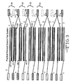
- FIG. 2 An arrangement of the top substrate electrodes 22, 23, 24 and 25 is illustrated in Fig. 2.
- the electrodes 22, 23, 24 and 25 are shaded to illustrate the electrode pattern.
- the top four electrodes form a first group of electrodes that is labeled 38.
- the group 38 includes a control electrode 25 at the top of the figure.
- the control electrode 25 also can be referred to as an auxiliary electrode or a second auxiliary electrode.
- the control electrode 25 is connected to a control electrode pad 25' that is on the left side of Fig. 2.
- the pad 25' provides an electrical connection between the control electrode 25 and a control voltage driver, as will be described below. Proceeding in a downward direction from the control electrode 25 in Fig.
- the next electrode in the first group 38 is a second sustainer electrode 23 that is connected to a second sustainer electrode pad 23' that also is on the left side of Fig. 2.
- the second sustainer electrode 23 also is labeled with a "Z”.
- adjacent to the second sustainer electrode 23 is a first sustainer electrode 22 that is connected to a first sustainer electrode pad 22' on the right side of Fig. 2.
- the first sustainer electrode 22 also is labeled with the letter "Y”.
- the bottom electrode in the first group 38 is a trigger electrode 24 which is connected to a trigger electrode pad 24' that also is on the right side of Fig. 2.
- the trigger electrode 24 also is labeled with the letter "T”.
- the trigger electrode 24 also can be referred to as an auxiliary electrode or a first auxiliary electrode.
- the orientation of the electrodes in the first group 38 is the same as shown in Fig. 1.
- the electrode orientation shown for the electrode group 38 repeats for the remaining groups of electrodes in Fig. 2.
- a second group of electrodes 40 immediately below the first group 38 has a control electrode 45 on top that is connected a control electrode pad 45' on the left side of Fig. 2.
- the second electrode from the top of the second group 40 is a second sustainer electrode 43 that is connected to a second sustainer electrode pad 43' on the left side of Fig. 2.
- the third electrode is a first sustainer electrode 42 that is connected to a first sustainer electrode pad 42' on the right, while the bottom electrode in the second group is a trigger electrode 44 connected to a trigger electrode pad 44', also on the right.
- the remaining electrodes in Fig. 2 are identified with the letters to show the pattern of electrodes.
- each of the individual electrode pads associated with the electrodes would be connected to a conventional plasma display panel voltage driver for selectively establishing plasma discharges within corresponding portions of the panel microgrooves 32.
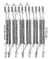
- the top group of electrodes in Fig. 3 is formed in the same order as the top group of electrodes shown in Fig. 2. Accordingly, the top group also is labeled 38 in Fig. 3 and the order of electrodes in a downward direction from the top is control electrode C, second sustainer electrode Z, first sustainer electrode Y and trigger electrode T.
- the second group of electrodes in Fig. 3 is labeled 50 and is formed upon the top substrate 12 as a mirror image of the first group 38.
- the top electrode in the second group 50 is a trigger electrode T and the second electrode from the top of the group 50 is a first sustainer electrode Y.
- the third electrode is a second sustainer electrode Z while the bottom electrode in the group 50 is a control electrode C.
- the electrode pads associated with the sustainer electrodes, Y and Z are on the right side of Fig. 3 while the electrode pads associated with the control and trigger electrodes, C and T, are on the left side of Fig. 3.
- the alternation of the electrode patterns in each group alternates throughout the display panel 10. Accordingly, the third group of electrodes 55 has the same pattern as the first group 38 while the fourth group 60 repeats the pattern of the second group 50.
- first and second sustainer electrodes can be electrically connected to a common electrode pad.
- first sustainer electrode 22 (Y) in the first electrode group 38 and the first sustainer electrode 42 (Y) in the second electrode group 50 are electrically connected to a common second sustainer electrode pad 62 (Y').
- second sustainer electrode 43 (Z) in the second electrode group 50 and second sustaining electrode 64 (Z) in the third electrode group 55 are electrically connected to a common second sustainer electrode pad 66 (Z').
- the present invention permits a significant reduction in the number of electrical connections and associated driver circuitry from prior art display panels. Therefore, the present invention contemplates a significant reduction in the cost of fabrication a plasma display panel 10.
- the drivers associated with the electrodes are illustrated in the plan view of the panel 10 shown in Fig. 4.
- the drawing of the panel in Fig. 4 has been simplified for clarity.
- the pattern of top substrate electrodes shown in Fig. 3 is repeated in Fig. 4 with the addition of address electrodes 32 and barrier ribs 34 that are formed on the bottom substrate 14.
- the address electrodes 32 and barrier ribs 34 are generally perpendicular to the top substrate electrodes.
- the address electrodes 32 are identified with the letter "X”.
- Fig. 4 is a schematic diagram of the electrode drivers.
- Six groups of bottom substrate electrodes and five address electrodes are shown in Fig. 4 and define a 6x5 array with 30 pixels. It will be appreciated that the circuitry shown in Fig. 4 can be also be applied to larger smaller arrays.
- Each of the drivers consists of a voltage supply which is selectively connected to associated electrodes through conventional switches.
- pairs of first sustainer electrodes Y are selectively connected through common electrode pads Y' and a conventional electronic switch labeled S Y to a first sustaining voltage supply labeled V Y .
- the first sustaining voltage supply generates first sustaining voltage waveforms that are described below.
- the logic circuitry for controlling the electronic switches has been omitted from Fig. 4.
- pairs of second sustaining electrodes Z are selectively connected through common electrode pads Z' and a conventional electronic switch labeled S z to a second sustaining voltage supply labeled V z .
- the second sustaining voltage supply V z generates second sustaining voltage waveforms that also are described below.
- the trigger electrodes T are selectively connected through electrode pads T' and individual conventional electronic switches labeled S T1 through S T6 to a trigger voltage supply labeled V T .
- the trigger voltage supply V T generates a trigger voltage waveform that is described below.
- the control electrodes C are selectively coupled through electrode pads C' and a conventional electronic switch labeled S c to a control voltage supply labeled V c .
- the address electrodes X are selectively connected through conventional electronic switches labeled S x1 through S x5 to an address voltage supply that is labeled V x .
- the address voltage supply V x generates address voltage waveforms that will be described below.
- sustaining voltage waveforms are applied simultaneously to pairs of first and second sustainer electrodes Y and Z in adjacent electrode groups during operation of the plasma display panel 10.
- the selective application of trigger voltage waveforms to the trigger electrodes T controls the establishment of plasma discharges with the display panel 10.
- FIG. 5 An alternate embodiment of the invention is illustrated in Fig. 5, where components that are similar to components shown in Fig. 3 have the same labels.
- the top substrate electrode pattern in Fig. 5 is the same as shown in Fig. 3; however, the connection of the electrodes to the electrode pads is different.
- adjacent pairs of trigger electrodes are connected to a common trigger electrode pad T' while adjacent pairs of control electrodes C are connected to a common control electrode pad C'.
- the number of trigger electrode pads T' is reduced by half while the number of control electrode pads C' are reduced by approximately half.
- pairs of the sustainer electrodes Y and Z are electrically connected to associated sustainer electrode pads Y' and Z', or Y" and Z", respectively, on the right side of Fig. 5, to control the discharge.
- the reduction in the number of trigger and control electrode pads, T' and C' again permits a significant reduction in the number of electrical connections and associated driver circuitry from prior art display panels. Therefore, the present invention contemplates a significant reduction in the cost of fabrication a plasma display panel 10.
- the drivers associated with the electrodes are illustrated for the alternate embodiment in the plan view of the panel 10 shown in Fig. 6.
- the drawing of the panel in Fig. 6 has been simplified for clarity.
- Components shown in Fig. 6 that are similar to components shown in Fig. 4 have the same labels.
- the drivers consist of a voltage supply selectively coupled to associated drivers through conventional electronic switches. While a 6x5 array is shown in Fig. 6, it will be appreciated that the invention also may be practiced on larger or smaller arrays.
- the number of electronic switches for the trigger electrodes T has been reduced from six, as shown in Fig. 4, to three. Additionally, the number of control electrodes has been reduced from six to four.
- trigger voltage waveforms are applied simultaneously to adjacent pairs of trigger electrodes T during operation of the plasma display panel 10. Because the trigger voltage is applied to adjacent pairs of trigger electrodes, the adjacent pairs of sustainer electrodes are supplied by separate sustaining voltage supplies connected through four electronic switches labeled S Z' , S Y' , S Z" and S Y" . Accordingly, both the trigger voltage and sustaining voltages must be present to establish a discharge in a particular pixel. Thus, the selective application of sustaining voltage waveforms to the sustaining electrode pairs, Y and Z cooperates with the trigger voltage to control the establishment of plasma discharges for specific pixels of the display panel 10. It will be appreciated that, while four sustaining voltage supplies are shown in Fig. 6, the invention also can be practiced with one voltage supply V Z supplying both Z electrode electronic switches S Z' and S Z" and one voltage supply V Y supplying both Y electrode electronic switches S Y . and S Y" (not shown).
- the present invention also contemplates a more efficient operation of the display panel 10.
- the operation of the PDP 10 will now be described in view of the voltage waveforms illustrated in Fig. 7.
- the same voltage waveforms are used for both circuit embodiments shown in Figs. 4 and 6.
- the voltage supplies generate voltage waveforms having the shapes shown while the electronic switches are selectively closed to apply the waveforms to the associated electrodes.
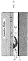
- the plasma display panel 10 is preconditioned between t 1 and t 2 .
- Preconditioning involves applying voltage waveforms of opposite polarities to the sustaining electrodes Y and Z and a negative going voltage to the trigger electrodes T. As a result, all wall charges are removed from the sides of the microgrooves 32.
- the preconditioning stage is used upon start up or when it is desired to totally clear the display panel 10, as when initiating a new display.
- the preconditioned state can be sustained by applying alternating voltages to the sustaining electrodes Y and Z as shown by the curves labeled V Y and V Z between t 2 and t 3 . While only one cycle of alternating sustaining voltages are illustrated in Fig. 7, the wall charge can be maintained for a longer time period by continuing the application of alternating voltages.
- the preconditioning and sustaining is often referred to as a "bulk erase" since the entire display panel 10 is cleared.
- the first and second sustainer voltages both go negative from t 3 to t 4 while the trigger voltage goes positive. As shown in Fig. 8, these voltages establish a brief plasma discharge 70 that extends transversely across the microgroove 32 between the trigger electrode T on the top substrate 12 and the opposite address electrode X on the bottom substrate 14.
- the plasma discharge 70 includes a cathode fall region 72 and a plasma plume 74.
- the plasma discharge 70 causes wall charges 76 to accumulate upon the adjacent sidewalls of the microgroove 32 containing the discharge 70.
- the sustainer electrode voltages resume alternating at t 4 , the plasma discharge 70 is extinguished; however, the wall charges 76 remain, as illustrated in Fig. 9.
- the wall charges are shown as dashed lines in the voltage waveforms labeled V Y -V Z and V T -V X in the lower portion of Fig. 7.
- the associated portion of the panel 10 is now prepared for writing. Accordingly, the portion of the voltage curves between t 1 and t 5 is often referred to as the "set-up" phase.
- the wall charge can be maintained by alternating the sustaining voltages V Y and V Z , as shown in Fig. 7 from t 5 to t 6 .
- the actual writing to illuminate a selected pixel begins.
- the voltage waveform applied to the address electrode X goes positive while the first and second sustainer voltages go negative and positive, respectively.
- a plasma discharge plume 80 is reestablished in the microgroove 32.
- the plume 80 arcs from the trigger and first sustainer electrodes T and Y laterally within the microgroove 32 to the second sustainer electrode Z.
- the plume 80 consists of ionized gas and includes positively charged ions and negatively charged electrons which excites the phosphor 38 deposited with the microgroove 32.
- the excited phosphor 38 emits visible light.
- the sustaining voltages resume alternating to sustain the plasma plume 80 and thereby the emission of light from the associated pixel, as illustrated in Fig. 11.
- a relatively low trigger voltage of less than 100 volts can initiate a plasma discharge 80 for a relatively high sustaining voltage of 280 to 380 volts, which is significantly greater than typical sustaining voltages of 180 to 200 volts as are known in the art.
- the higher sustaining voltage drives the plasma discharge 80 deeper into the channel, as shown in Figs. 10 and 11.
- the deeper penetration of the discharge 80 into the microgroove 32 results in additional phosphor 38 being excited, which, in turn, yields a brighter display.
- the higher sustaining voltage improve the efficiency of the panel 10 by reducing the amount of current required to power the display.
- the invention contemplates separate trigger and sustaining voltage supplies V T , V Y , and V Z .
- the same voltage supply was typically utilized to supply both the trigger and sustaining voltages. This not only increased the complexity of the switching circuitry, but also limited the magnitude of the sustaining voltages. Accordingly, provision of a separate trigger voltage supply V T allows increasing the sustaining voltage magnitudes as described above.
- the initial portion of the set-up erases the cells in the panel. Similar sustaining and trigger voltages can be applied to selected electrodes to erase a particular cell. However, the erasing typically generates a brief low level illumination of the cell. The low level illumination can reduce the contrast of the image appearing on the panel 10. Accordingly, the invention also contemplates applying ramped sustaining voltages (not shown) to eliminate the illumination during the erase operation. The ramped voltages result in a localized wall charge 86, as shown in Fig. 12.
- the invention further contemplates applying control voltage waveforms to the panel 10.
- control voltage waveforms are generated by the control voltage supply V c and applied through a single conventional electronic switch S c , as illustrated by the circuit diagrams shown in Figs. 4 and 6.
- the associated control voltage waveforms are shown as the top curve in Fig. 7.
- the control voltage waveforms supplement the sustainer voltages to assure that the plasma plume 80 is urged deeply into the microgroove 32 and to otherwise control the shape of the plume 80.
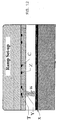
- the present invention also contemplates a method for selectively erasing selected pixels on a plasma display panel.
- the voltages applied to the panel electrodes to erase a pixel are illustrated in Fig. 13.
- Fig. 13 it is assumed that a plasma discharge exists and is being sustained from t 8 through t 9 .
- the times shown along the horizontal axis in the figure continue the times shown in preceding Fig. 7.
- a selective erase is initiated.
- the voltages on the sustaining electrodes, Y and Z are reduced to zero and held at zero while pulses are applied to the trigger and address electrodes, T and X, for the specific pixel.
- the trigger and electrode pulses cooperate with the reduced sustainer electrode voltages to erase the illuminated pixel.
- the erased cell retains the wall charges necessary to reestablish a plasma discharge; however, the voltages applied to the electrodes are insufficient to trigger another discharge. It would be necessary for the voltages applied to the sustaining electrodes, Y and Z, to be held at opposite voltages while pulses are applied to the corresponding trigger and address electrodes, T and X, as shown from t 6 to t 7 in Fig. 7, to restart the plasma discharge. Thus, the erase step leaves the cell in condition for re-initiation of the discharge.
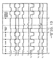
- the present invention further contemplates an alternate circuit embodiment of the PDP illustrated in Figs. 3 and 4.
- the alternate embodiment is shown in Fig. 14 where the sustaining electrodes Y and Z in adjacent electrode groups are connected together and supplied by a single contact pad Y' and Z'. While the electrodes are in a different sequence from top to bottom of Fig. 14 than shown in Figs. 3 and 4, it will be noted that the adjacent groups of sustainer electrodes Y and Z, trigger electrode T and control electrode C are arranged as mirror images of one another. Additionally, it is contemplated that the circuit connections shown in Fig. 14 also can be applied to the PDP electrode orientation shown in Fig. 3.
- the top Y electrode in Fig. 14 has a right end 13 connected through the electronic switch S Y to sustaining voltage supply labeled V Y and a left end connected to the left end of the Y electrode in the second electrode group from the top of the figure.
- the top Z electrode has a left end connected to the left end of the Z electrode in the second group from the top of the figure.
- the Z electrode in the second group also has a right end connected through the electronic switch S z to the sustaining voltage supply labeled V z .
- the connections shown to the sustaining voltage supplies V z and V Y not only reduce the number of contact pads and simplify the driver circuits but also compensate for voltage drops in the sustaining electrodes Z and Y.
Landscapes
- Engineering & Computer Science (AREA)
- Physics & Mathematics (AREA)
- Plasma & Fusion (AREA)
- Chemical & Material Sciences (AREA)
- Materials Engineering (AREA)
- Gas-Filled Discharge Tubes (AREA)
- Control Of Indicators Other Than Cathode Ray Tubes (AREA)
- Control Of Gas Discharge Display Tubes (AREA)
Applications Claiming Priority (2)
| Application Number | Priority Date | Filing Date | Title |
|---|---|---|---|
| US629118 | 2000-07-31 | ||
| US09/629,118 US6597120B1 (en) | 1999-08-17 | 2000-07-31 | Flat-panel display with controlled sustaining electrodes |
Publications (2)
| Publication Number | Publication Date |
|---|---|
| EP1178512A2 true EP1178512A2 (de) | 2002-02-06 |
| EP1178512A3 EP1178512A3 (de) | 2007-11-21 |
Family
ID=24521646
Family Applications (1)
| Application Number | Title | Priority Date | Filing Date |
|---|---|---|---|
| EP01118278A Withdrawn EP1178512A3 (de) | 2000-07-31 | 2001-07-30 | Flache Plasma-Anzeigetafel mit gesteuerten Plasma-Aufrechterhaltungselektroden |
Country Status (5)
| Country | Link |
|---|---|
| EP (1) | EP1178512A3 (de) |
| JP (1) | JP2002100294A (de) |
| KR (1) | KR20020011121A (de) |
| CN (1) | CN1269094C (de) |
| MX (1) | MXPA01007699A (de) |
Families Citing this family (4)
| Publication number | Priority date | Publication date | Assignee | Title |
|---|---|---|---|---|
| JP2004192875A (ja) | 2002-12-10 | 2004-07-08 | Nec Plasma Display Corp | プラズマディスプレイパネル及びその駆動方法 |
| FR2857144A1 (fr) * | 2003-07-03 | 2005-01-07 | Thomson Plasma | Procede de pilotage d'un panneau a plasma a declenchement matriciel echelonne |
| KR100795813B1 (ko) * | 2006-12-29 | 2008-01-21 | 삼성에스디아이 주식회사 | 플라즈마 디스플레이 패널 |
| CN102244967A (zh) * | 2011-05-16 | 2011-11-16 | 浙江大华技术股份有限公司 | 智能交通领域闪光灯信号分路触发装置及方法 |
Family Cites Families (5)
| Publication number | Priority date | Publication date | Assignee | Title |
|---|---|---|---|---|
| RU2089966C1 (ru) * | 1995-11-22 | 1997-09-10 | Научно-производственная компания "Орион-Плазма" - Совместная акционерная компания закрытого типа | Газоразрядная индикаторная панель переменного тока с реверсивным поверхностным разрядом |
| KR19980046358A (ko) * | 1996-12-12 | 1998-09-15 | 엄길용 | 플라즈마 디스플레이 패널 구조 및 그 구동방법 |
| RU2120154C1 (ru) * | 1997-03-28 | 1998-10-10 | Совместное закрытое акционерное общество "Научно-производственная компания "ОРИОН-ПЛАЗМА" | Газоразрядная индикаторная панель переменного тока с поверхностным разрядом и способ управления ею |
| JPH10333636A (ja) * | 1997-03-31 | 1998-12-18 | Mitsubishi Electric Corp | プラズマディスプレイパネル |
| CN1165938C (zh) * | 1997-08-19 | 2004-09-08 | 松下电器产业株式会社 | 气体放电板 |
-
2001
- 2001-07-30 MX MXPA01007699A patent/MXPA01007699A/es unknown
- 2001-07-30 EP EP01118278A patent/EP1178512A3/de not_active Withdrawn
- 2001-07-31 KR KR1020010046271A patent/KR20020011121A/ko not_active Ceased
- 2001-07-31 CN CNB011237813A patent/CN1269094C/zh not_active Expired - Fee Related
- 2001-07-31 JP JP2001232538A patent/JP2002100294A/ja active Pending
Also Published As
| Publication number | Publication date |
|---|---|
| KR20020011121A (ko) | 2002-02-07 |
| CN1269094C (zh) | 2006-08-09 |
| EP1178512A3 (de) | 2007-11-21 |
| CN1345018A (zh) | 2002-04-17 |
| MXPA01007699A (es) | 2004-08-11 |
| JP2002100294A (ja) | 2002-04-05 |
Similar Documents
| Publication | Publication Date | Title |
|---|---|---|
| EP0691671A1 (de) | Entladungs-Anzeigegerät | |
| US6825606B2 (en) | Flat plasma display panel with independent trigger and controlled sustaining electrodes | |
| US6597120B1 (en) | Flat-panel display with controlled sustaining electrodes | |
| JPH11265661A (ja) | プラズマ表示パネル | |
| US6459201B1 (en) | Flat-panel display with controlled sustaining electrodes | |
| US6603266B1 (en) | Flat-panel display | |
| JP2000357463A (ja) | 交流型プラズマディスプレイパネル,プラズマディスプレイ装置及び交流型プラズマディスプレイパネルの駆動方法 | |
| EP1178512A2 (de) | Flache Plasma-Anzeigetafel mit gesteuerten Plasma-Aufrechterhaltungselektroden | |
| US7379032B2 (en) | Plasma display device | |
| KR100625496B1 (ko) | 플라즈마 디스플레이 패널 | |
| JP3111949B2 (ja) | 面放電型プラズマディスプレイパネルおよびその駆動方法 | |
| US6549180B1 (en) | Plasma display panel and driving method thereof | |
| JP4205281B2 (ja) | プラズマディスプレイ装置 | |
| KR100324261B1 (ko) | 플라즈마 디스플레이 패널 및 그 구동방법 | |
| KR100298556B1 (ko) | 고주파를이용한플라즈마디스플레이패널및그의구동방법 | |
| JP3492889B2 (ja) | プラズマディスプレイパネルの駆動方法 | |
| KR100357236B1 (ko) | 고주파를이용한플라즈마디스플레이패널및그구동방법 | |
| JP3005002B2 (ja) | プラズマディスプレイパネル | |
| KR100442234B1 (ko) | 플라즈마디스플레이패널및그방전방법 | |
| US7768199B2 (en) | Plasma display-panel comprising a reduced-section discharge expansion zone | |
| KR100269396B1 (ko) | 칼라 플라즈마 디스플레이 패널 | |
| JP2005050675A (ja) | プラズマ表示装置及びプラズマディスプレイパネルの駆動方法 | |
| JP2001084914A (ja) | 高周波駆動プラズマディスプレーパネルとその製造方法及びそれを駆動するための駆動装置 | |
| KR100293515B1 (ko) | 고주파를이용한플라즈마디스플레이패널의구동방법 | |
| KR910009632B1 (ko) | 트리거전극을 갖는 면방전형 플라즈마 평면 표시판 |
Legal Events
| Date | Code | Title | Description |
|---|---|---|---|
| PUAI | Public reference made under article 153(3) epc to a published international application that has entered the european phase |
Free format text: ORIGINAL CODE: 0009012 |
|
| AK | Designated contracting states |
Kind code of ref document: A2 Designated state(s): AT BE CH CY DE DK ES FI FR GB GR IE IT LI LU MC NL PT SE TR |
|
| AX | Request for extension of the european patent |
Free format text: AL;LT;LV;MK;RO;SI |
|
| RAP1 | Party data changed (applicant data changed or rights of an application transferred) |
Owner name: LG ELECTRONICS, INC. |
|
| PUAL | Search report despatched |
Free format text: ORIGINAL CODE: 0009013 |
|
| AK | Designated contracting states |
Kind code of ref document: A3 Designated state(s): AT BE CH CY DE DK ES FI FR GB GR IE IT LI LU MC NL PT SE TR |
|
| AX | Request for extension of the european patent |
Extension state: AL LT LV MK RO SI |
|
| STAA | Information on the status of an ep patent application or granted ep patent |
Free format text: STATUS: THE APPLICATION IS DEEMED TO BE WITHDRAWN |
|
| 18D | Application deemed to be withdrawn |
Effective date: 20080201 |