EP1178596A1 - Dispositif onduleur - Google Patents
Dispositif onduleur Download PDFInfo
- Publication number
- EP1178596A1 EP1178596A1 EP00902877A EP00902877A EP1178596A1 EP 1178596 A1 EP1178596 A1 EP 1178596A1 EP 00902877 A EP00902877 A EP 00902877A EP 00902877 A EP00902877 A EP 00902877A EP 1178596 A1 EP1178596 A1 EP 1178596A1
- Authority
- EP
- European Patent Office
- Prior art keywords
- circuit part
- voltage
- high withstand
- inverter
- withstand voltage
- Prior art date
- Legal status (The legal status is an assumption and is not a legal conclusion. Google has not performed a legal analysis and makes no representation as to the accuracy of the status listed.)
- Granted
Links
Images




Classifications
-
- H—ELECTRICITY
- H02—GENERATION; CONVERSION OR DISTRIBUTION OF ELECTRIC POWER
- H02M—APPARATUS FOR CONVERSION BETWEEN AC AND AC, BETWEEN AC AND DC, OR BETWEEN DC AND DC, AND FOR USE WITH MAINS OR SIMILAR POWER SUPPLY SYSTEMS; CONVERSION OF DC OR AC INPUT POWER INTO SURGE OUTPUT POWER; CONTROL OR REGULATION THEREOF
- H02M7/00—Conversion of AC power input into DC power output; Conversion of DC power input into AC power output
- H02M7/42—Conversion of DC power input into AC power output without possibility of reversal
- H02M7/44—Conversion of DC power input into AC power output without possibility of reversal by static converters
- H02M7/48—Conversion of DC power input into AC power output without possibility of reversal by static converters using discharge tubes with control electrode or semiconductor devices with control electrode
- H02M7/53—Conversion of DC power input into AC power output without possibility of reversal by static converters using discharge tubes with control electrode or semiconductor devices with control electrode using devices of a triode or transistor type requiring continuous application of a control signal
- H02M7/537—Conversion of DC power input into AC power output without possibility of reversal by static converters using discharge tubes with control electrode or semiconductor devices with control electrode using devices of a triode or transistor type requiring continuous application of a control signal using semiconductor devices only, e.g. single switched pulse inverters
- H02M7/5387—Conversion of DC power input into AC power output without possibility of reversal by static converters using discharge tubes with control electrode or semiconductor devices with control electrode using devices of a triode or transistor type requiring continuous application of a control signal using semiconductor devices only, e.g. single switched pulse inverters in a bridge configuration
- H02M7/53871—Conversion of DC power input into AC power output without possibility of reversal by static converters using discharge tubes with control electrode or semiconductor devices with control electrode using devices of a triode or transistor type requiring continuous application of a control signal using semiconductor devices only, e.g. single switched pulse inverters in a bridge configuration with automatic control of output voltage or current
-
- H—ELECTRICITY
- H02—GENERATION; CONVERSION OR DISTRIBUTION OF ELECTRIC POWER
- H02M—APPARATUS FOR CONVERSION BETWEEN AC AND AC, BETWEEN AC AND DC, OR BETWEEN DC AND DC, AND FOR USE WITH MAINS OR SIMILAR POWER SUPPLY SYSTEMS; CONVERSION OF DC OR AC INPUT POWER INTO SURGE OUTPUT POWER; CONTROL OR REGULATION THEREOF
- H02M7/00—Conversion of AC power input into DC power output; Conversion of DC power input into AC power output
- H02M7/42—Conversion of DC power input into AC power output without possibility of reversal
- H02M7/44—Conversion of DC power input into AC power output without possibility of reversal by static converters
- H02M7/48—Conversion of DC power input into AC power output without possibility of reversal by static converters using discharge tubes with control electrode or semiconductor devices with control electrode
- H02M7/53—Conversion of DC power input into AC power output without possibility of reversal by static converters using discharge tubes with control electrode or semiconductor devices with control electrode using devices of a triode or transistor type requiring continuous application of a control signal
- H02M7/537—Conversion of DC power input into AC power output without possibility of reversal by static converters using discharge tubes with control electrode or semiconductor devices with control electrode using devices of a triode or transistor type requiring continuous application of a control signal using semiconductor devices only, e.g. single switched pulse inverters
- H02M7/538—Conversion of DC power input into AC power output without possibility of reversal by static converters using discharge tubes with control electrode or semiconductor devices with control electrode using devices of a triode or transistor type requiring continuous application of a control signal using semiconductor devices only, e.g. single switched pulse inverters in a push-pull configuration
-
- H—ELECTRICITY
- H02—GENERATION; CONVERSION OR DISTRIBUTION OF ELECTRIC POWER
- H02M—APPARATUS FOR CONVERSION BETWEEN AC AND AC, BETWEEN AC AND DC, OR BETWEEN DC AND DC, AND FOR USE WITH MAINS OR SIMILAR POWER SUPPLY SYSTEMS; CONVERSION OF DC OR AC INPUT POWER INTO SURGE OUTPUT POWER; CONTROL OR REGULATION THEREOF
- H02M1/00—Details of apparatus for conversion
- H02M1/32—Means for protecting converters other than automatic disconnection
Definitions
- the present invention relates to an inverter device, and relates more particularly to an inverter device having a circuit for preventing improper operation and voltage breakdown of a high withstand voltage IC used for drive control of a bridge circuit formed from switching elements driving a load.
- conventional inverter devices have a clamp diode connected between a high voltage reference terminal and low voltage reference terminal of a high withstand voltage IC used for drive controlling switching elements as a means for handling negative surges resulting from line inductance and current variation per unit time di/dt when switching a switching element driving a load.
- Fig. 8 is a schematic circuit diagram showing connection of the above-noted clamp diode. It should be noted that Fig. 8 shows only the peripheral circuits of one exemplary high withstand voltage IC, for example, the high withstand voltage IC for switching control of switching elements driving a load connected to the external connection terminal U to which the load is connected.
- Clamp diode 102 is connected between high voltage side reference terminal Vs and low voltage side reference terminal VSS of high withstand voltage IC 101; high withstand voltage IC 101 controls operation of switching element 104 connected between external power supply terminal P to which a positive supply voltage is applied, and external terminal U to which a load is connected.
- the high withstand voltage IC controlling operation of switching element 105 connected between external terminal U and external power supply terminal N to which a negative supply voltage is applied is omitted in this figure.
- Voltage V (Vs - VSS) is held by clamp diode 102 to the forward voltage of clamp diode 102 only when a negative potential surge causes voltage V (Vs - VSS) between high voltage side reference terminal Vs and low voltage side reference terminal VSS to become a negative voltage.
- the present invention resolves the above described problem, and an object of this invention is to provide an inverter apparatus capable of preventing breakdown and improper operation of a high withstand voltage IC that controls the switching operation of switching elements for driving a load.
- An inverter apparatus includes an inverter circuit part for inverter driving a load.
- This inverter circuit part has at least a pair of switching 'elements connected in series in a forward direction between both polarity terminals of a dc supply for supplying power to a load.
- An inverter drive circuit part is employed for driving each switching element of the inverter circuit part and has at least one high withstand voltage IC wherein the signal level reference potential is different in the input signal and output signal.
- a clamping circuit part clamps the potential of the low voltage side reference terminal, to which a potential that is a reference for operation of the high withstand voltage IC in the inverter drive circuit part and is a reference for a signal on the low potential side of the high withstand voltage IC is applied, to the high voltage reference terminal to ' which is applied a reference potential for the high potential-side signal in the high withstand voltage IC.
- the inverter apparatus also includes a voltage dividing circuit part for voltage dividing a voltage between the low voltage side reference terminal of the high withstand voltage IC in the inverter drive circuit part and the negative electrode of the dc supply.
- the voltage dividing circuit part can also be disposed to each high withstand voltage IC.
- the voltage dividing circuit part is an element functioning as a voltage dividing resistance connected between the low voltage side reference terminal of the high withstand voltage IC in the inverter drive circuit part and the negative electrode of the dc supply, in which case the voltage dividing circuit part is an element effecting a voltage dividing resistance, such as one resistor or one inductance.
- the low voltage side reference terminal of the high withstand voltage IC in the inverter drive circuit part is connected by way of a diode to elements functioning as the clamping circuit part and voltage dividing resistance, and current flows from the voltage dividing resistance in the direction of the low voltage reference terminal of the high withstand voltage IC.
- bypass circuit part for bypassing the voltage dividing circuit part is disposed to each voltage dividing circuit part so that high withstand voltage IC operating current output from the low voltage reference terminal flows to the negative electrode of the dc supply.
- this bypass circuit part is a bypass diode for bypassing the voltage dividing circuit part, and the bypass circuit part comprises one bypass diode.
- Fig. 1 is a schematic circuit diagram showing an example of an inverter apparatus according to a first embodiment of the present invention. It should be noted that Fig. 1 shows an example of a three-phase inverter apparatus.
- three-phase inverter apparatus 1 comprises a voltage inverter 2 comprising six IGBT switching elements Q1 to Q6 and parallel connected diodes D1 to D6 corresponding to switching elements Q1 to Q6, and an inverter drive circuit 3 for driving the voltage inverter.
- collectors of switching elements Q1 to Q3 are each connected to external power supply terminal P for applying a positive supply voltage to voltage inverter 2, at that time a corresponding line inductance Lc1 to Lc3 is formed between the collector and external power supply terminal P.
- Emitters of switching elements Q4 to Q6 are connected to the external power supply terminal N for applying a negative supply voltage to voltage inverter 2, at that time a corresponding line inductance Le4 to Le6 is formed between each emitter and the external power supply terminal N.
- the emitter of switching element Q1 and the collector of switching element Q4 are each connected to external connection terminal U for connecting a load, and line inductance Le1 between the emitter and external connection terminal U, and line inductance Lc4 between the collector and external connection terminal U, are respectively formed.
- the emitter of switching element Q2 and the collector of switching element Q5 are each connected to external connection terminal V for connecting a load, and line inductance Le2 between the emitter and external connection terminal V, and line inductance Lc5 between the collector and external connection terminal V, are respectively formed.
- the emitter of switching element Q3 and the collector of switching element Q6 are each connected to external connection terminal W for connecting a load, and line inductance Le3 between the emitter and external connection terminal W, and line inductance Lc6 between the collector and external connection terminal W, are respectively formed.
- switching elements Q1 to Q6 are connected to inverter drive circuit 3 by way of intervening corresponding resistors R1 to R6; inverter drive circuit 3 controls switching of switching elements Q1 to Q6 according to an input control signal.
- a dc supply VDC is connected between external power supply terminal P and external power supply terminal N, and a reactor (not shown in the figures) is connected as a load to external connection terminals U, V, W.
- High withstand voltage ICs 11 to 16 for driving switching elements Q1 to Q6 are disposed in inverter drive circuit 3 for each switching element Q1 to Q6 of the voltage inverter 2, and a clamp diode D11 to D16 is disposed between the high voltage side reference terminal Vs and low voltage side reference terminal VSS of each high withstand voltage IC 11 to 16 so that the direction from low voltage side reference terminal VSS to high voltage side reference terminal Vs is forward.
- the low voltage side reference terminal VSS of each high withstand voltage IC 11 to 16 is connected by way of intervening protection circuit 21, comprising voltage-dividing resistance R21 and bypass diode D21 parallel connected to voltage-dividing resistance R21, to external power supply terminal N and to external ground terminal GND.
- Control signal input terminal IN of each high withstand voltage IC 11 to 16 is respectively connected to a corresponding external control signal input terminal Up, Vp, Wp, Un, Vn, Wn, and positive supply input terminal VCC and low voltage side reference terminal VSS functioning as the negative supply input terminal are respectively connected to the positive and negative electrodes of dc supply 22.
- high withstand voltage ICs 11 to 16 all have the same circuit configuration, the internal circuitry of only high withstand voltage IC 13 is shown in Fig. 1, and the internal circuitry of high withstand voltage ICs 11, 12, and 14 to 16 is omitted. As a result, the operation of high withstand voltage IC 13 is described below, and further description of the operation of the other high withstand voltage ICs is omitted because their operation is the same as that of high withstand voltage IC 13.
- High withstand voltage IC 13 comprises an input buffer 25, n-channel MOS transistor (referred to below as “NMOS transistor") 26, resistor R27, and driver circuit 28.
- the input terminal of input buffer 25 is connected to control signal input terminal IN, the output terminal is connected to the gate of NMOS transistor 26, the positive supply input terminal is connected to positive supply input terminal VCC, and the negative supply input terminal is connected to low voltage side reference terminal VSS.
- NMOS transistor 26 The drain of NMOS transistor 26 is connected to resistor R27 and the input terminal of driver circuit 28, and the source of NMOS transistor 26 is connected to low voltage side reference terminal VSS.
- NMOS transistor 26 and resistor R27 form a level shifter 29 for shifting the output signal of input buffer 25 to generate a signal of a floating potential floating from the potential of the output signal.
- driver circuit 28 the output terminal is connected to output terminal OUT of high withstand voltage IC 13
- the positive supply input terminal is connected to positive floating supply input terminal Vb
- the negative supply input terminal is connected to high voltage side reference terminal Vs functioning as the negative floating supply input terminal.
- the input buffer 25, driver circuit 28, and level shifter 29 thus form a level shifting circuit.
- a corresponding dc source 31 to 36 is connected between positive floating supply input terminal Vb and high voltage side reference terminal Vs in each high withstand voltage IC 11 to 16.
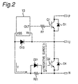
- Fig. 2 being a circuit diagram showing the peripheral circuits to high withstand voltage IC 13 in Fig. 1. It should be noted that the line inductances are omitted in Fig. 2.
- a reactor as a load is connected to external connection terminals U to W; the negative potential surge (referred to below as “negative surge") caused between external connection terminal U and external power supply terminal N as a result of switching switching element Q1, for example, is voltage divided by voltage-dividing resistance R21 and clamp diode D13 of protection circuit 21.
- a high withstand voltage IC for driving switching elements Q1 to Q6 is described by way of example with reference to Fig.1 and Fig. 2, but the invention shall not be so limited and can be applied to a high withstand voltage IC used for switching element drive control.
- the invention can be applied to a level shift circuit for driving a switching element, and a high withstand voltage IC comprising a level shift circuit functioning as an overcurrent detection circuit for detecting overcurrent flow to a switching element.
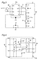
- Fig. 3 shows another example of an inverter apparatus according to this first embodiment in this case
- Fig. 4 shows an exemplary circuit for the high withstand voltage IC shown in Fig. 3.
- FIG. 3 shows an example of the high withstand voltage IC connected to switching element Q1 of inverter apparatus 1 shown in Fig. 1 and peripheral circuitry, and other high withstand voltage ICs and peripheral circuits are omitted because they are the same.
- Fig. 3 and Fig. 4 like parts are identified by the same reference numerals shown in Fig. 1, and further description thereof is omitted below where only the differences from Fig. 1 are described.
- Fig. 3 and Fig. 1 Differences between Fig. 3 and Fig. 1 are that the emitters of switching elements Q1 to Q3 are connected to corresponding external connection terminals U to W by way of intervening current detection resistors R41 to R43, and the emitters of switching elements Q4 to Q6 are connected to external power supply terminal N by way of intervening current detection resistors R44 to R46, the internal circuits of high withstand voltage ICs 11 to 16 in Fig. 1 are changed, and NOR gates N41 to N46 are added.
- one input terminal to NOR gates N41 to N46 is an inverting input terminal for inverting the input signal level, and the other input terminal is a non-inverting input terminal that does not invert the input signal level.
- the control signal input terminals IN of high withstand voltage ICs 11a to 16a are connected to the output terminal of corresponding NOR gates N41 to N46, and the non-inverting input terminals of NOR gates N41 to N46 are respectively connected to corresponding external control signal input terminals Up, Vp, Wp, Un, Vn, Wn.
- the node between the emitter of each switching element Q1 to Q6 and the corresponding resistor R41 to R46 is connected to input terminal Fin of high withstand voltage ICs 11a to 16a, and the corresponding output terminal Fout of high withstand voltage ICs 11a to 16a is connected to the inverting input terminal of the corresponding NOR gate N41 to N46.
- high withstand voltage IC 13a The operation of high withstand voltage IC 13a is described below using Fig. 4, and because operation of the other high withstand voltage ICs 11a, 12a, and 14a to 16a is the same as high withstand voltage IC 13a, further description thereof is omitted below.
- High withstand voltage IC 13a comprises input buffers 25 and 41, NMOS transistor 26, p-channel MOS transistor (referred to below as “PMOS transistor") 42, resistors R27 and R47, and driver circuits 28 and 44.
- PMOS transistor p-channel MOS transistor
- resistors R27 and R47 resistors 28 and 44.
- input buffer 41 the input terminal is connected to input terminal Fin
- the output terminal is connected to the gate of PMOS transistor 42
- the positive supply input terminal is connected to positive floating supply input terminal Vb
- the negative supply input terminal is connected to high voltage side reference terminal Vs.
- the drain of PMOS transistor 42 is connected to resistor R47 and the input terminal of driver circuit 44, and the source of PMOS transistor 42 is connected to positive floating supply input terminal Vb.
- PMOS transistor 42 and resistor R47 form level shifter 49 for down shifting the output signal from input buffer 41 and generating a signal of a potential referenced to the ground level.
- driver circuit 44 the output terminal is connected to output terminal Fout of high withstand voltage IC 13a, the positive supply input terminal is connected to positive supply input terminal VCC, and the negative supply input terminal is connected to low voltage side reference terminal VSS.
- the input buffer 25, driver circuit 28, and level shifter 29 thus form a level shift circuit for shifting the input signal level up
- input buffer 41, driver circuit 44, and level shifter 49 form a level shift circuit for shifting the input signal level down.
- high withstand voltage IC 13a drives switching element Q1 according to a control signal input from external control signal input terminal Up through NOR gate 43 to the corresponding control signal input terminal IN, and from the voltage obtained from resistor R41 detects an overcurrent flowing to switching 'element Q1. If an overcurrent flows to switching element Q1, a high level signal is input to input terminal Fin of high withstand voltage IC 13a, and high withstand voltage IC 13a outputs a low level signal from output terminal Fout while this high level signal is input.
- An inverter apparatus thus has a protection circuit 21 comprising bypass diode D21 parallel connected to a voltage-dividing resistance R21 disposed between low voltage side reference terminal VSS of the high withstand voltage IC and external power supply terminal N for applying a negative supply voltage to voltage inverter 2. It is therefore possible by adding a simple circuit to prevent a negative voltage applied between the high voltage side reference terminal Vs and low voltage side reference terminal VSS of each high withstand voltage IC from dropping below the minimum rated withstand voltage between the terminals due to a negative surge produced when switching a switching element, and it is therefore possible to inexpensively prevent improper operation and withstand voltage breakdown of the high withstand voltage IC.
- One protection circuit 21 protects against breakdown of each high withstand voltage IC due to a negative surge in the above-described first embodiment, but a protection circuit 21 can be disposed to each high withstand voltage IC, and a configuration of this type is described next as a second embodiment of the present invention.
- Fig. 5 is a schematic circuit diagram showing an inverter apparatus according to a second embodiment of the present invention. It should be noted that like parts are identified by like reference numerals in Fig. 5 and Fig. 1. Further description thereof is thus omitted here, and only the differences therebetween are described.
- Fig. 5 and Fig. 1 The differences in Fig. 5 and Fig. 1 are that in place of protection circuit 21 in Fig. 1 protection circuits 61 to 66, each comprising a bypass diode and parallel connected voltage-dividing resistor, are disposed to high withstand voltage IC 11 to 16, respectively.
- inverter drive circuit 3 in Fig. 1 is referred to as inverter drive circuit 53
- inverter apparatus 1 in Fig. 1 is inverter apparatus 51.
- inverter apparatus 51 comprises voltage inverter 2 and inverter drive circuit 53.
- Inverter drive circuit 53 comprises high withstand voltage ICs 11 to 16, clamp diodes D11 to D16, dc supplies 22 and 31 to 36, and protection circuits 61 to 66.
- Each protection circuit 61 to 66 is a circuit having a voltage-dividing resistor and parallel connected bypass diode, and in each protection circuit 61 to 66 a corresponding voltage dividing resistor R61 to R66 is parallel connected to a corresponding bypass diode D61 to D66.
- each protection circuit 61 to 66 has the same circuit configuration, the operation of protection circuit 63 is described below, and the operation of protection circuits 61, 62, and 64 to 66 is not described because it is the same as protection circuit 63.
- Protection circuit 63 is connected between low voltage side reference terminal VSS and external power supply terminal N of high withstand voltage IC 13; more specifically, the node between voltage dividing resistor R63 and the anode of bypass diode D63 is connected to low voltage side reference terminal VSS of high withstand voltage IC 13, and the node between voltage dividing resistor R63 and bypass diode D63 is connected to external power supply terminal N.
- a reactor constituting a load is connected to external connection terminals U to W, and a negative surge caused between external connection terminal U and external power supply terminal N as a result of switching switching element Q1, for example, is voltage divided by resistance R63 and clamp diode D13 of protection circuit 63.
- a circuit diagram excerpting the peripheral circuits of high withstand voltage IC 13 in Fig. 5 is the same as that shown in Fig. 2 except that protection circuit 21 is replaced by protection circuit 63, and is described below referring to Fig. 2 and substituting protection circuit 63 for protection circuit 21.
- a corresponding protection circuit 61 to 66 is connected between each low voltage side reference terminal VSS and external power supply terminal N of high withstand voltage ICs 11 to 16, and a closed loop to the ground line is formed by adding voltage-dividing resistance R61 to R66 in protection circuits 61 to 66. Because this closed loop is related to improper operation of the high withstand voltage IC in some cases, a corresponding diode D71 to D76 can be connected as shown in Fig. 6 between the nodes between clamp diodes D11 to D16 and protection circuits 61 to 66, and the low voltage side reference terminal VSS of the corresponding high withstand voltage IC 11 to 16.
- the anode of diode 73 is connected to low voltage side reference terminal VSS of high withstand voltage IC 13, and the cathode of diode 73 is connected to the anode of clamp diode D13 and the node between voltage dividing resistor R63 and the anode of bypass diode D63.
- formation of a closed loop from external power supply terminal N through low voltage side reference terminal VSS to external power supply terminal N can be prevented, voltage fluctuation in low voltage side reference terminal VSS of high withstand voltage IC 13 resulting from a closed loop can be prevented, and improper operation of high withstand voltage IC 13 can be prevented.
- the other high withstand voltage ICs 11, 12, and 14 to 16 are the same, and description thereof is omitted.
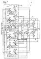
- bypass diodes D61 to D66 can be omitted as shown in Fig. 7.
- this second embodiment is described using by way of example a high withstand voltage IC for driving switching elements Q1 to Q6, but as described in the first embodiment above the invention can be applied to a high withstand voltage IC used for switching element drive control, for example, a level shift circuit for driving a switching element and a high withstand voltage IC comprising a level shift circuit functioning as an overcurrent detection circuit for detecting overcurrent flow to a switching element.
- an inverter apparatus disposes protection circuits 61 to 66 each having a parallel connected voltage dividing resistance and bypass diode between low voltage side reference terminal VSS of each high withstand voltage IC 11 to 16 and external power supply terminal N for applying a negative supply voltage to the voltage inverter 2. It is therefore possible to prevent a negative voltage applied between the high voltage side reference terminal Vs and low voltage side reference terminal VSS of each high withstand voltage IC from dropping below the minimum rated withstand voltage between the terminals due to a negative surge produced when switching a switching element, and it is therefore possible to reliably prevent improper operation and withstand voltage breakdown of the high withstand voltage IC.
- the present invention can provide an inverter apparatus capable of preventing withstand voltage breakdown and improper operation of a high withstand voltage IC used for switching element drive control as a result of a negative surge produced when switching a switching element of the inverter.
Landscapes
- Engineering & Computer Science (AREA)
- Power Engineering (AREA)
- Inverter Devices (AREA)
Applications Claiming Priority (1)
| Application Number | Priority Date | Filing Date | Title |
|---|---|---|---|
| PCT/JP2000/000712 WO2001059918A1 (fr) | 2000-02-09 | 2000-02-09 | Dispositif onduleur |
Publications (3)
| Publication Number | Publication Date |
|---|---|
| EP1178596A1 true EP1178596A1 (fr) | 2002-02-06 |
| EP1178596A4 EP1178596A4 (fr) | 2004-06-02 |
| EP1178596B1 EP1178596B1 (fr) | 2009-02-04 |
Family
ID=11735670
Family Applications (1)
| Application Number | Title | Priority Date | Filing Date |
|---|---|---|---|
| EP00902877A Expired - Lifetime EP1178596B1 (fr) | 2000-02-09 | 2000-02-09 | Dispositif onduleur |
Country Status (5)
| Country | Link |
|---|---|
| US (1) | US6459598B1 (fr) |
| EP (1) | EP1178596B1 (fr) |
| JP (1) | JP3577478B2 (fr) |
| DE (1) | DE60041514D1 (fr) |
| WO (1) | WO2001059918A1 (fr) |
Cited By (2)
| Publication number | Priority date | Publication date | Assignee | Title |
|---|---|---|---|---|
| US7924064B2 (en) | 2003-11-28 | 2011-04-12 | Mitsubishi Denki Kabushiki Kaisha | Inverter circuit |
| EP3264588A4 (fr) * | 2016-04-27 | 2018-05-09 | Mitsubishi Electric Corporation | Dispositif d'attaque de moteur, dispositif à cycle de réfrigération, et climatiseur |
Families Citing this family (11)
| Publication number | Priority date | Publication date | Assignee | Title |
|---|---|---|---|---|
| JP3992922B2 (ja) * | 2000-11-27 | 2007-10-17 | シャープ株式会社 | 液晶表示装置用基板及びその製造方法及びそれを備えた液晶表示装置 |
| FR2841342B1 (fr) * | 2002-06-21 | 2004-10-29 | Thales Ultrasonics Sas | Structure d'entree pour echographie a ultrasons |
| JP3983622B2 (ja) | 2002-08-08 | 2007-09-26 | 三菱電機株式会社 | パワーデバイス駆動回路 |
| JP4675910B2 (ja) * | 2005-01-14 | 2011-04-27 | 三菱電機株式会社 | インバータ装置 |
| JP4992876B2 (ja) * | 2008-09-30 | 2012-08-08 | 三菱電機株式会社 | インバータ装置 |
| US7990743B2 (en) | 2009-10-20 | 2011-08-02 | General Electric Company | System and method for decreasing solar collector system losses |
| US7855906B2 (en) | 2009-10-26 | 2010-12-21 | General Electric Company | DC bus voltage control for two stage solar converter |
| US8050062B2 (en) | 2010-02-24 | 2011-11-01 | General Electric Company | Method and system to allow for high DC source voltage with lower DC link voltage in a two stage power converter |
| JP5999677B2 (ja) * | 2011-09-20 | 2016-09-28 | ローム株式会社 | 電子回路 |
| JP6304966B2 (ja) * | 2013-08-05 | 2018-04-04 | 三菱電機株式会社 | 半導体駆動装置及び半導体装置 |
| US10116310B2 (en) | 2014-12-17 | 2018-10-30 | Mitsubishi Electric Corporation | Level shift circuit, integrated circuit, and power semiconductor module |
Family Cites Families (8)
| Publication number | Priority date | Publication date | Assignee | Title |
|---|---|---|---|---|
| US3832621A (en) * | 1971-12-27 | 1974-08-27 | Gen Electric | Reliable static power converter with control logic |
| US3919621A (en) * | 1974-11-27 | 1975-11-11 | Motorola Inc | Control system for inverter circuits |
| US4331886A (en) * | 1980-06-23 | 1982-05-25 | International Business Machines Corporation | Current switch driving circuit arrangements |
| US4414479A (en) * | 1981-07-14 | 1983-11-08 | General Electric Company | Low dissipation snubber for switching power transistors |
| US5418707A (en) * | 1992-04-13 | 1995-05-23 | The United States Of America As Represented By The United States Department Of Energy | High voltage dc-dc converter with dynamic voltage regulation and decoupling during load-generated arcs |
| US5532712A (en) * | 1993-04-13 | 1996-07-02 | Kabushiki Kaisha Komatsu Seisakusho | Drive circuit for use with transmissive scattered liquid crystal display device |
| JP3560737B2 (ja) | 1996-07-23 | 2004-09-02 | 三菱電機株式会社 | インバータ装置 |
| SG66453A1 (en) * | 1997-04-23 | 1999-07-20 | Int Rectifier Corp | Resistor in series with bootstrap diode for monolithic gate device |
-
2000
- 2000-02-09 WO PCT/JP2000/000712 patent/WO2001059918A1/fr not_active Ceased
- 2000-02-09 US US09/958,270 patent/US6459598B1/en not_active Expired - Lifetime
- 2000-02-09 JP JP2001559132A patent/JP3577478B2/ja not_active Expired - Lifetime
- 2000-02-09 EP EP00902877A patent/EP1178596B1/fr not_active Expired - Lifetime
- 2000-02-09 DE DE60041514T patent/DE60041514D1/de not_active Expired - Lifetime
Cited By (4)
| Publication number | Priority date | Publication date | Assignee | Title |
|---|---|---|---|---|
| US7924064B2 (en) | 2003-11-28 | 2011-04-12 | Mitsubishi Denki Kabushiki Kaisha | Inverter circuit |
| DE102004057187B4 (de) * | 2003-11-28 | 2014-01-23 | Mitsubishi Denki K.K. | Inverterschaltung |
| EP3264588A4 (fr) * | 2016-04-27 | 2018-05-09 | Mitsubishi Electric Corporation | Dispositif d'attaque de moteur, dispositif à cycle de réfrigération, et climatiseur |
| US11031900B2 (en) | 2016-04-27 | 2021-06-08 | Mitsubishi Electric Corporation | Motor drive apparatus, refrigeration cycle apparatus and air conditioner |
Also Published As
| Publication number | Publication date |
|---|---|
| EP1178596A4 (fr) | 2004-06-02 |
| DE60041514D1 (de) | 2009-03-19 |
| US6459598B1 (en) | 2002-10-01 |
| WO2001059918A1 (fr) | 2001-08-16 |
| JP3577478B2 (ja) | 2004-10-13 |
| EP1178596B1 (fr) | 2009-02-04 |
Similar Documents
| Publication | Publication Date | Title |
|---|---|---|
| KR101863014B1 (ko) | 자기 소호형 반도체 소자의 단락 보호 회로 | |
| CN101689799B (zh) | 功率元件的驱动电路 | |
| EP1178596A1 (fr) | Dispositif onduleur | |
| US11144082B2 (en) | Gate driver circuit for reducing deadtime inefficiencies | |
| US20210242864A1 (en) | Switch circuit capable of overcurrent protection with small and simple circuit, and with simple operation, without affecting normal operation | |
| US4841166A (en) | Limiting shoot-through current in a power MOSFET half-bridge during intrinsic diode recovery | |
| US5909135A (en) | High-side MOSFET gate protection shunt circuit | |
| CN101282115A (zh) | 多沟道半导体集成电路 | |
| US11595039B2 (en) | Power switching circuit and corresponding method of operation | |
| JPWO2001059918A1 (ja) | インバータ装置 | |
| JPH06153533A (ja) | レベルシフト回路及びこれを用いたインバータ装置 | |
| EP0810731B1 (fr) | Circuit d'attaque de transistor commandé en tension | |
| CN109285726B (zh) | 具有温度保护的用于对电感器进行放电的放电电路 | |
| JP5133648B2 (ja) | 電圧制御形スイッチングデバイスのゲート駆動装置 | |
| JP4003833B2 (ja) | 電界制御型半導体素子の駆動回路 | |
| US6680630B1 (en) | Driver circuit for power device | |
| JP3258050B2 (ja) | 誘導性負荷用mosfetを備えた回路装置 | |
| JP2002033648A (ja) | 縦続接続回路 | |
| EP0459457A2 (fr) | Circuit d'attaque de sortie | |
| JP7094181B2 (ja) | 負荷駆動回路 | |
| JP3039092B2 (ja) | 短絡保護回路 | |
| US7319359B2 (en) | High current charge pump for intelligent power switch drive | |
| JP3477566B2 (ja) | 過電流保護機能を有するゲート駆動回路 | |
| JP4640680B2 (ja) | トランジスタブリッジの駆動方法及びその回路 | |
| JP3824602B2 (ja) | スイッチング制御装置及びスイッチング制御方法 |
Legal Events
| Date | Code | Title | Description |
|---|---|---|---|
| PUAI | Public reference made under article 153(3) epc to a published international application that has entered the european phase |
Free format text: ORIGINAL CODE: 0009012 |
|
| 17P | Request for examination filed |
Effective date: 20011024 |
|
| AK | Designated contracting states |
Kind code of ref document: A1 Designated state(s): AT BE CH CY DE DK ES FI FR GB GR IE IT LI LU MC NL PT SE |
|
| RBV | Designated contracting states (corrected) |
Designated state(s): DE FR IT |
|
| A4 | Supplementary search report drawn up and despatched |
Effective date: 20040419 |
|
| RIC1 | Information provided on ipc code assigned before grant |
Ipc: 7H 03K 17/08 A Ipc: 7H 02M 7/5387 B |
|
| RTI1 | Title (correction) |
Free format text: INVERTER DEVICE |
|
| RAP1 | Party data changed (applicant data changed or rights of an application transferred) |
Owner name: MITSUBISHI DENKI KABUSHIKI KAISHA |
|
| 17Q | First examination report despatched |
Effective date: 20060901 |
|
| 17Q | First examination report despatched |
Effective date: 20060901 |
|
| GRAP | Despatch of communication of intention to grant a patent |
Free format text: ORIGINAL CODE: EPIDOSNIGR1 |
|
| GRAS | Grant fee paid |
Free format text: ORIGINAL CODE: EPIDOSNIGR3 |
|
| GRAA | (expected) grant |
Free format text: ORIGINAL CODE: 0009210 |
|
| AK | Designated contracting states |
Kind code of ref document: B1 Designated state(s): DE FR IT |
|
| REF | Corresponds to: |
Ref document number: 60041514 Country of ref document: DE Date of ref document: 20090319 Kind code of ref document: P |
|
| PLBE | No opposition filed within time limit |
Free format text: ORIGINAL CODE: 0009261 |
|
| STAA | Information on the status of an ep patent application or granted ep patent |
Free format text: STATUS: NO OPPOSITION FILED WITHIN TIME LIMIT |
|
| 26N | No opposition filed |
Effective date: 20091105 |
|
| PGFP | Annual fee paid to national office [announced via postgrant information from national office to epo] |
Ref country code: FR Payment date: 20110315 Year of fee payment: 12 Ref country code: IT Payment date: 20110208 Year of fee payment: 12 |
|
| REG | Reference to a national code |
Ref country code: DE Ref legal event code: R084 Ref document number: 60041514 Country of ref document: DE Effective date: 20120425 |
|
| REG | Reference to a national code |
Ref country code: FR Ref legal event code: ST Effective date: 20121031 |
|
| PG25 | Lapsed in a contracting state [announced via postgrant information from national office to epo] |
Ref country code: IT Free format text: LAPSE BECAUSE OF NON-PAYMENT OF DUE FEES Effective date: 20120209 |
|
| PG25 | Lapsed in a contracting state [announced via postgrant information from national office to epo] |
Ref country code: FR Free format text: LAPSE BECAUSE OF NON-PAYMENT OF DUE FEES Effective date: 20120229 |
|
| PGFP | Annual fee paid to national office [announced via postgrant information from national office to epo] |
Ref country code: DE Payment date: 20190129 Year of fee payment: 20 |
|
| PGFP | Annual fee paid to national office [announced via postgrant information from national office to epo] |
Ref country code: DE Payment date: 20190129 Year of fee payment: 20 |
|
| REG | Reference to a national code |
Ref country code: DE Ref legal event code: R071 Ref document number: 60041514 Country of ref document: DE |