EP1179904A1 - Verfahren und vorrichtung zur radio nachrichtenübertragung - Google Patents
Verfahren und vorrichtung zur radio nachrichtenübertragung Download PDFInfo
- Publication number
- EP1179904A1 EP1179904A1 EP01914174A EP01914174A EP1179904A1 EP 1179904 A1 EP1179904 A1 EP 1179904A1 EP 01914174 A EP01914174 A EP 01914174A EP 01914174 A EP01914174 A EP 01914174A EP 1179904 A1 EP1179904 A1 EP 1179904A1
- Authority
- EP
- European Patent Office
- Prior art keywords
- radio communication
- chip
- data
- communication apparatus
- frequency
- Prior art date
- Legal status (The legal status is an assumption and is not a legal conclusion. Google has not performed a legal analysis and makes no representation as to the accuracy of the status listed.)
- Withdrawn
Links
Images








Classifications
-
- H—ELECTRICITY
- H04—ELECTRIC COMMUNICATION TECHNIQUE
- H04L—TRANSMISSION OF DIGITAL INFORMATION, e.g. TELEGRAPHIC COMMUNICATION
- H04L27/00—Modulated-carrier systems
- H04L27/26—Systems using multi-frequency codes
-
- H—ELECTRICITY
- H04—ELECTRIC COMMUNICATION TECHNIQUE
- H04L—TRANSMISSION OF DIGITAL INFORMATION, e.g. TELEGRAPHIC COMMUNICATION
- H04L1/00—Arrangements for detecting or preventing errors in the information received
- H04L1/004—Arrangements for detecting or preventing errors in the information received by using forward error control
- H04L1/0056—Systems characterized by the type of code used
- H04L1/0071—Use of interleaving
-
- H—ELECTRICITY
- H04—ELECTRIC COMMUNICATION TECHNIQUE
- H04B—TRANSMISSION
- H04B1/00—Details of transmission systems, not covered by a single one of groups H04B3/00 - H04B13/00; Details of transmission systems not characterised by the medium used for transmission
- H04B1/69—Spread spectrum techniques
- H04B1/692—Hybrid techniques using combinations of two or more spread spectrum techniques
-
- H—ELECTRICITY
- H04—ELECTRIC COMMUNICATION TECHNIQUE
- H04B—TRANSMISSION
- H04B1/00—Details of transmission systems, not covered by a single one of groups H04B3/00 - H04B13/00; Details of transmission systems not characterised by the medium used for transmission
- H04B1/69—Spread spectrum techniques
- H04B1/707—Spread spectrum techniques using direct sequence modulation
-
- H—ELECTRICITY
- H04—ELECTRIC COMMUNICATION TECHNIQUE
- H04B—TRANSMISSION
- H04B7/00—Radio transmission systems, i.e. using radiation field
- H04B7/24—Radio transmission systems, i.e. using radiation field for communication between two or more posts
- H04B7/26—Radio transmission systems, i.e. using radiation field for communication between two or more posts at least one of which is mobile
- H04B7/2628—Radio transmission systems, i.e. using radiation field for communication between two or more posts at least one of which is mobile using code-division multiple access [CDMA] or spread spectrum multiple access [SSMA]
-
- H—ELECTRICITY
- H04—ELECTRIC COMMUNICATION TECHNIQUE
- H04L—TRANSMISSION OF DIGITAL INFORMATION, e.g. TELEGRAPHIC COMMUNICATION
- H04L5/00—Arrangements affording multiple use of the transmission path
- H04L5/003—Arrangements for allocating sub-channels of the transmission path
- H04L5/0044—Allocation of payload; Allocation of data channels, e.g. PDSCH or PUSCH
-
- H—ELECTRICITY
- H04—ELECTRIC COMMUNICATION TECHNIQUE
- H04L—TRANSMISSION OF DIGITAL INFORMATION, e.g. TELEGRAPHIC COMMUNICATION
- H04L5/00—Arrangements affording multiple use of the transmission path
- H04L5/02—Channels characterised by the type of signal
- H04L5/023—Multiplexing of multicarrier modulation signals, e.g. multi-user orthogonal frequency division multiple access [OFDMA]
- H04L5/026—Multiplexing of multicarrier modulation signals, e.g. multi-user orthogonal frequency division multiple access [OFDMA] using code division
Definitions
- the present invention relates to a radio communication apparatus and radio communication method for use in a digital communication system, and more particularly to a radio communication apparatus and radio communication method that perform radio communications with a combination of a multicarrier modulation method such as the OFDM (Orthogonal Frequency Division Multiplexing) modulation method, and a CDMA (Code Division Multiple Access) method.
- a multicarrier modulation method such as the OFDM (Orthogonal Frequency Division Multiplexing) modulation method
- CDMA Code Division Multiple Access
- Multicarrier modulation methods such as the OFDM modulation method are drawing attention as one kind of technology for combating frequency selective fading.
- a multicarrier modulation method is a technology for effectively performing high-speed transmission by transmitting data using a plurality of carriers (subcarriers) whose speed is suppressed to a level at which frequency selective fading does not occur.
- the OFDM modulation method in particular, the subcarriers on which data is placed are mutually orthogonal, making this the multicarrier modulation method offering the highest spectral efficiency.
- the OFDM modulation method can be implemented with a comparatively simple hardware configuration. For these reasons, various studies are being undertaken concerning the OFDM modulation method as a frequency selective fading countermeasure.
- a spread spectrum method is another technology for combating frequency selective fading.
- a spread spectrum method is a technology that improves interference immunity by spreading a signal along the frequency axis by means of a spreading code called a PN code to obtain spreading gain.
- Spread spectrum methods include a direct spreading method and a frequency hopping method. Of these, a CDMA (Code Division Multiple Access ) method using direct spreading has been decided on for use in the next-generation mobile communication system IMT-2000.
- OFDM-CDMA methods combining the OFDM modulation method and CDMA method have recently been a focus of attention. OFDM-CDMA methods are broadly divided into time domain spreading and frequency domain spreading. Time domain spreading and frequency domain spreading methods are described below.
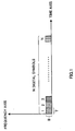
- FIG.1 is a diagram showing the state of digital symbols before modulation processing
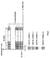
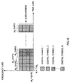
- FIG.2 is a diagram showing the chip arrangement after modulation processing using the time domain spreading method.
- N digital symbols serial data stream
- M spreading code
- IFFT sequential inverse fast Fourier transform
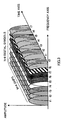
- the OFDM symbol signal pattern generated by the time domain spreading method is as shown in FIG.3.
- the time domain spreading method eight digital symbols differentiated by black-and-white shading on the frequency axis are assigned sequentially, one chip at a time, each to a different one of subcarriers f1 through f8, and eight OFDM symbols are generated at t0 through t7.
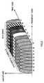
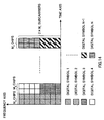
- FIG.4 is a diagram showing the arrangement of chips after modulation processing using the frequency domain spreading method.
- a serial data stream comprising N digital symbols (serial data stream) (FIG. 1) are multiplied, one symbol at a time, by a spreading code with spreading factor M.
- chips undergo sequential IFFT processing one symbol at a time with M chips in parallel.
- N OFDM symbols with M subcarriers are generated. That is, with frequency domain spreading, after spreading, chips are arranged along the frequency axis at their respective times (FIG.4). In other words, after spreading, chips are arranged on different subcarriers.
- the OFDM symbol signal pattern generated by the frequency domain spreading method is as shown in FIG.5.
- the frequency domain spreading method eight OFDM symbols are generated sequentially at t0 through t7 for eight digital symbols differentiated by black-and-white shading on the time axis.
- the eight chips for each digital symbol are assigned each to a different one of subcarriers f1 through f8.
- a statistical multiplexing effect is the ability to accommodate more user signals when data presence occurs randomly according to the user than in the case of continuous transmission according to a decrease in energy in an interval in which there is no reciprocal transmission.
- a plurality of chips after spreading of a particular digital symbol that are conventionally arranged one-dimensionally, aligned either on the frequency axis or on the time axis are arranged two-dimensionally, distributed both on the frequency axis and on the time axis.
- a particular data item is arranged two-dimensionally, distributed both on the frequency axis and on the time axis, by spreading data on the time axis, and shifting each post-spreading chip step-wise in the carrier frequency upward or downward direction on the frequency axis, changing the arrangement.
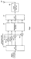
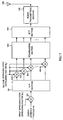
- FIG.6 is a block diagram showing the configuration of the transmitting side in a radio communication apparatus according to Embodiment 1 of the present invention.
- the transmitting side radio communication apparatus shown in FIG.6 comprises a serial/parallel conversion section (S/P section) 101, time domain spreaders 102-1 through 102-N, rearranging section 103, inverse fast Fourier transform section (IFFT section) 104, radio transmitting section 105, and antenna 106.
- S/P section serial/parallel conversion section
- IFFT section inverse fast Fourier transform section
- FIG.7 is a block diagram showing the configuration of the receiving side in a radio communication apparatus according to Embodiment 1 of the present invention.
- the receiving side radio communication apparatus shown in FIG.7 comprises an antenna 201, radio receiving section 202, Fourier transform section (FFT section) 203, arrangement restoration section 204, time domain despreaders 205-1 through 205-N, RAKE sections 206-1 through 206-N, and parallel/serial conversion section (P/S section) 207.
- FFT section Fourier transform section
- arrangement restoration section 204 time domain despreaders 205-1 through 205-N
- RAKE sections 206-1 through 206-N RAKE sections 206-1 through 206-N
- P/S section parallel/serial conversion section
- the radio communication apparatus shown in FIG.6 is provided with N time domain spreaders
- the radio communication apparatus shown in FIG.7 is provided with N time domain despreaders and RAKE sections.
- N digital symbols 1 through N (serial data stream) shown in FIG.1 are converted to parallel data streams by the S/P section 101, and each of these is input to the corresponding time domain spreader. That is, digital symbol 1 is input to time domain spreader 102-1, digital symbol 2 is input to time domain spreader 102-2, and so on through to digital symbol N which is input to time domain spreader 102-N.
- time domain spreaders 102-1 through 102-N digital symbols 1 through N are spread by means of a spreading code with spreading factor M. That is, digital symbols 1 through N are spread to M chips on the time axis. More specifically, digital symbol 1 is spread to t0 through tM time chips by time domain spreader 102-1, digital symbol 2 is spread to t0 through tM time chips by time domain spreader 102-2, and so on through to digital symbol N which is spread to t0 through tM time chips by time domain spreader 102-N.
- the post-spreading data of M chips is input to the rearranging section 103.
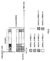
- chip arrangement data is stored in the rearranging section 103 as shown in FIG.2. That is, data of N symbols is stored in the frequency axis direction, and data of M chips is stored in the time axis direction.
- each post-spreading chip undergoes rearrangement by being shifted step-wise in the carrier frequency upward or downward direction on the frequency axis.
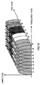
- digital symbol 1 will be considered, taking the case where a shift is made in the carrier frequency upward direction. That is, chips 1 through M of digital symbol 1 spread in the time axis direction are shifted one step at a time in the carrier frequency upward direction as shown in FIG.8. This kind of shift processing is carried out on chips 1 through M of digital symbols 1 through N.
- chips are input sequentially to the IFFT section 104 with N in parallel, and undergo IFFT processing.
- OFDM symbols are generated with chip 1 of digital symbol 1 assigned to subcarrier 1, chip 1 of digital symbol 2 assigned to subcarrier 2, and so on through to chip 1 of digital symbol N which is assigned to subcarrier N, and then OFDM symbols are generated with chip 2 of digital symbol N assigned to subcarrier 1, chip 2 of digital symbol 1 assigned to subcarrier 2, and so on through to chip 2 of digital symbol N-1 which is assigned to subcarrier N.
- M such OFDM symbols are generated. That is, a particular digital symbol is arranged two-dimensionally, distributed both on the frequency axis and on the time axis.
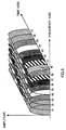
- the OFDM symbol signal pattern generated by the IFFT section 104 is as shown in FIG.9.
- eight digital symbols differentiated by black-and-white shading are assigned sequentially, with the elapse of time, one chip at a time, each to a different one of subcarriers f1 through f8, and eight OFDM symbols are generated at t0 through t7.
- the eight chips into which digital symbol 1 is spread are arranged respectively at time t0 of frequency f1, time t1 of frequency f2, time t2 of frequency f3, time t3 of frequency f4, time t4 of frequency f5, time t5 of frequency f6, time t6 of frequency f7, and time t7 of frequency f8.
- each chip of digital symbols 2 through 8 is arranged step-wise ahead of digital symbol 1.
- the chips of digital symbol 2 are arranged at time t0 of frequency f2, time t1 of frequency f3, time t2 of frequency f4, time t3 of frequency f5, time t4 of frequency f6, time t5 of frequency f7, and time t6 of frequency f8.
- one chip uses a time width of N ⁇ T/M and a frequency band width of M ⁇ B/N. That is, the interval between subcarriers in OFDM symbol shown in FIG.9 is M ⁇ B/N. Therefore, the area occupied by each digital symbol in the time-frequency domain is M ⁇ T ⁇ B, M times the area occupied by one digital symbol prior to modulation processing.
- M OFDM symbols generated by the IFFT section 104 are input sequentially to the radio transmitting section 105, and after undergoing predetermined radio processing such as up-conversion, are transmitted from the antenna 106.
- predetermined radio processing such as down-conversion is carried out by the radio receiving section 202 on OFDM symbols received via the antenna 201.
- OFDM symbols are input to the FFT section 203.
- Signals of digital symbols 1 through N transmitted by means of subcarriers 1 through N are then extracted by having FFT processing performed on the OFDM symbols by the FFT section 203. Similar processing is performed for M OFDM symbols received sequentially, and the resulting signals are input to the arrangement restoration section 204.
- the arrangement restoration section 204 performs rearrangement that is the reverse of the rearrangement performed by the rearranging section 103 in the transmitting side radio communication apparatus.
- the arrangement of chips is restored to what it was prior to rearrangement by the rearranging section 103. That is, the arrangement of chips is restored to the arrangement shown in FIG.2.
- the chips are input, N in parallel, to time domain despreaders 205-1 through 205-N and despread. After despreading, the data streams are input to RAKE sections 206-1 through 206-N, respectively.
- RAKE sections 206-1 through 206-N perform RAKE combination processing that gathers together and combines delay path components along the time axis . That is, RAKE combination for digital symbol 1 is performed by RAKE section 206-1, RAKE combination for digital symbol 2 is performed by RAKE section 206-2, and so on through to RAKE combination for digital symbol N performed by RAKE section 206-N. After RAKE combination, digital symbols are input to the P/S section 207.
- data (digital symbols) assigned to a plurality of subcarriers of different frequencies by means of S/P conversion are spread in the time elapse direction, and post-spreading chips are shifted step-wise in the carrier frequency upward or downward direction on the frequency axis, changing the arrangement, after which OFDM symbols are generated by IFFT processing.
- data that has undergone FFT processing is restored to its arrangement prior to being rearranged on the transmitting side, and this restored data is despread in the time elapse direction.
- each item of data after despreading includes a plurality of components with different times and different frequencies.
- a frequency diversity effect is obtained.
- multipath separation is possible at OFDM symbol precision, and consequently RAKE combination is possible, enabling multipath distortion to be reduced. That is to say, a path diversity effect is obtained.
- a particular digital symbol is arranged two-dimensionally, distributed both on the frequency axis and on the time axis, by having each chip that has been spread on the time axis shifted step-wise in the carrier frequency upward or downward direction on the frequency axis.
- the method of distribution on the frequency axis is not limited to this, and any distribution method may be used as long as it is a method of distribution on the frequency axis based on a predetermined rule.
- a particular data item is arranged two-dimensionally, distributed both on the frequency axis and on the time axis, by spreading data in both the frequency domain and time domain-that is, by spreading data in both the frequency axis direction and time axis direction.
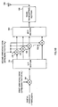
- FIG. 10 is a block diagram showing the configuration of the transmitting side in a radio communication apparatus according to Embodiment 2 of the present invention.
- the transmitting side radio communication apparatus shown in FIG.10 comprises a frequency domain spreader 301, S/P section 101, time domain spreaders 102-1 through 102-M 1 , IFFT section 104, radio transmitting section 105, and antenna 106.
- Parts in FIG.10 identical to those in Embodiment 1 (FIG.6) are assigned the same codes as in FIG.6 and their detailed explanations are omitted.
- FIG.11 is a block diagram showing the configuration of the receiving side in a radio communication apparatus according to Embodiment 2 of the present invention.
- the receiving side radio communication apparatus shown in FIG.11 comprises an antenna 201, radio receiving section 202, FFT section 203, time domain despreaders 205-1 through 205-M 1 , RAKE sections 206-1 through 206-M 1 , P/S section 207, and frequency domain despreader 401.
- Parts in FIG.11 identical to those in Embodiment 1 (FIG.7) are assigned the same codes as in FIG.7 and their detailed explanations are omitted.
- the radio communication apparatus shown in FIG.10 is provided with M 1 time domain spreaders
- the radio communication apparatus shown in FIG. 11 is provided with M 1 time domain despreaders and RAKE sections.
- N digital symbols 1 through N are spread by the frequency domain spreader 301 by means of a first spreading code with spreading factor M 1 .
- the post-spreading data of M 1 chips is input to the S/P section 101.
- data of M 1 chips input serially is converted to parallel data.
- digital symbols 1 through N are spread to M 1 chips on the frequency axis, and as a result, chips 1 through M 1 are assigned to subcarriers 1 through M 1 , respectively, each of a different frequency.
- the M 1 chips converted to parallel form by the S/P section 101 are input to the respective corresponding time domain spreaders. That is, the first chip of each digital symbol is input to time domain spreader 102-1, the second chip is input to time domain spreader 102-2, and so on through to the M 1 'th chip which is input to time domain spreader 102-M 1 .
- time domain spreaders 102-1 through 102-M 1 chips 1 through M 1 are further spread by means of a second spreading code with spreading factor M 2 . That is, the digital symbols spread to M 1 chips on the frequency axis are further spread to M 2 chips on the time axis.
- each digital symbol is spread by M 1 ⁇ M 2 times, that is, M 1 times in the frequency domain and M 2 times in the time domain.
- a particular digital symbol is arranged two-dimensionally, distributed both on the frequency axis and on the time axis.
- Chips spread by time domain spreaders 102-1 through 102-M 1 are input sequentially to the IFFT section 104, M 1 in parallel, and undergo IFFT processing. As a result, N ⁇ M 2 OFDM symbols are generated by the IFFT section 104.
- the chip arrangement on the frequency axis and time axis is as shown in FIG.12. That is, digital symbols 1 through N are arranged sequentially for four chips in the frequency axis direction and for two chips in the time axis direction.
- the OFDM symbol signal pattern generated by the IFFT section 104 is as shown in FIG.13. That is, the eight chips into which digital symbol 1 is spread are arranged respectively at time t0 of frequency f1, time t0 of frequency f2, time t0 of frequency f3, time t0 of frequency f4, time t1 of frequency f1, time t1 of frequency f2, time t1 of frequency f3, and time t1 of frequency f4. Similarly, each chip of digital symbols 2 through 8, also, is arranged after digital symbol 1.
- the chips of digital symbol 2 are arranged at time t2 of frequency f1, time t2 of frequency f2, time t2 of frequency f3, time t2 of frequency f4, time t3 of frequency f1, time t3 of frequency f2, time t3 of frequency f3, and time t3 of frequency f4.
- OFDM symbols are input to the FFT section 203.
- Signals transmitted by means of subcarriers 1 through M 1 are then extracted by having FFT processing performed on the OFDM symbols by the FFT section 203. Similar processing is performed for N ⁇ M 2 OFDM symbols received sequentially, and the resulting signals are input to time domain despreaders 205-1 through 205-M 1 .
- despreading processing is carried out on the input data by means of the same second spreading code (spreading factor M 2 ) used by time domain spreaders 102-1 through 102-M 1 in the transmitting side radio communication apparatus. That is, despreading processing is performed in the time domain.
- the data is RAKE-combined by RAKE sections 206-1 through 206-M 1 , and then converted to a serial data stream by the P/S section 207 and input to the frequency domain despreader 401.
- despreading processing is carried out on the input data by means of the same first spreading code (spreading factor M 1 ) used by the frequency domain spreader 301 in the transmitting side radio communication apparatus.
- RAKE-combined digital symbols 1 through N are obtained sequentially.
- the number of time domain spreaders required in the transmitting side radio communication apparatus, and the number of time domain despreaders and RAKE sections required in the receiving side radio communication apparatus is X ⁇ M 1 . That is, X ⁇ M 1 subcarriers are included in one OFDM symbol.
- the S/P section in the transmitting side radio communication apparatus outputs in parallel chips of digital symbol 1 and digital symbol 2 spread M 1 times respectively. That is to say, 2 ⁇ M 1 chips are output in parallel.
- digital symbol 1 and digital symbol 2 are simultaneously spread to M 1 chips each on the frequency axis. Then each chip is further spread to M 2 chips on the time axis by a time domain spreader 102.
- the chip arrangement on the frequency axis and time axis is as shown in FIG.14. That is, digital symbols spread to 4 ⁇ 2 chips are arranged in parallel two digital symbols at a time on the frequency axis.
- the OFDM symbol signal pattern generated by the IFFT section 104 is as shown in FIG.15. That is, the eight chips into which digital symbol 1 is spread are arranged respectively at time t0 of frequency f1, time t0 of frequency f2, time t0 of frequency f3, time t0 of frequency f4, time t1 of frequency f5, time t1 of frequency f6, time t1 of frequency f7, and time t1 of frequency f8.
- the chips of digital symbol 2 are arranged at time t0 of frequency f5, time t0 of frequency f6, time t0 of frequency f7, time t0 of frequency f8, time t1 of frequency f5, time t1 of frequency f6, time t1 of frequency f7, and time t1 of frequency f8.
- time domain spreading processing is performed after frequency domain spreading processing.
- this order may be reversed. That is to say, a particular digital symbol can still be arranged two-dimensionally, distributed on the frequency axis and time axis, if frequency domain spreading processing is performed after time domain spreading processing.
- post-spreading chips are further shifted step-wise in the carrier frequency upward or downward direction on the frequency axis, changing the arrangement.
- FIG.17 is a block diagram showing the configuration of the transmitting side in a radio communication apparatus according to Embodiment 3 of the present invention.
- the transmitting side radio communication apparatus shown in FIG.17 is configured with the further provision of a rearranging section 103 as described in Embodiment 1 between time domain spreaders 102-1 through 102-M 1 and IFFT section 104 of a radio communication apparatus according to Embodiment 2 (FIG.10).
- Parts in FIG.17 identical to those in Embodiment 1 (FIG.6) or Embodiment 2 (FIG.10) are assigned the same codes as in FIG.6 or FIG.10 and their detailed explanations are omitted.
- FIG.18 is a block diagram showing the configuration of the receiving side in a radio communication apparatus according to Embodiment 3 of the present invention.
- the receiving side radio communication apparatus shown in FIG.18 is configured with the further provision of an arrangement restoration section 204 as described in Embodiment 1 between the FFT section 203 and time domain despreaders 205-1 through 205-M 1 of a radio communication apparatus according to Embodiment 2 (FIG.11).
- Parts in FIG.18 identical to those in Embodiment 1 (FIG.7) or Embodiment 2 (FIG.11) are assigned the same codes as in FIG.7 or FIG.11 and their detailed explanations are omitted.
- the resulting OFDM symbol signal pattern is as shown in FIG.19.
- a case is shown where four digital symbols are transmitted in parallel.
- data that has undergone a Fourier transform is restored by the arrangement restoration section 204 to its arrangement prior to being rearranged by the rearranging section 103, and is then despread in both the frequency domain and time domain.
- post-spreading chips are arranged irregularly both on the frequency axis and on the time axis.
- FIG.20 is a block diagram showing the configuration of the transmitting side in a radio communication apparatus according to Embodiment 4 of the present invention.
- the transmitting side radio communication apparatus shown in FIG.20 comprises a spreader 501, chip interleaver 502, S/P section 101, IFFT section 104, radio transmitting section 105, and antenna 106.
- Parts in FIG.20 identical to those in Embodiment 1 (FIG.6) are assigned the same codes as in FIG.6 and their detailed explanations are omitted.
- FIG.21 is a block diagram showing the configuration of the receiving side in a radio communication apparatus according to Embodiment 4 of the present invention.
- the receiving side radio communication apparatus shown in FIG.21 comprises an antenna 201, radio receiving section 202, FFT section 203, P/S section 207, chip de-interleaver 601, and despreader 602. Parts in FIG.21 identical to those in Embodiment 1 (FIG.7) are assigned the same codes as in FIG.7 and their detailed explanations are omitted.
- N digital symbols 1 through N are spread by the spreader 501 by means of a spreading code with spreading factor M.
- chips are input sequentially to the chip interleaver 502.
- N ⁇ M chips are stored in the chip interleaver 502.
- chip interleaver 502 chip interleaving (rearrangement of the chip series) with a predetermined pattern is performed so that chips are arranged irregularly both on the frequency axis and on the time axis, as shown in FIG.22 for example.
- M chips of a particular digital symbol are arranged irregularly both on the frequency axis and on the time axis.
- chips are input to the S/P section and converted to parallel form.
- chips are input to the chip de-interleaver 601.
- chip de-interleaver 601 rearrangement is performed that is the reverse of the rearrangement carried out by the chip interleaver 502 on the transmitting side.
- the chip series is restored to what it was prior to rearrangement by the chip interleaver 502.
- chips are input to the despreader 602, and are despread using the same spreading code (spreading factor M) as was used by the spreader 501 on the transmitting side.
- chip interleaving is carried out whereby, following spreading, chips are arranged irregularly both on the frequency axis and on the time axis.
- the interleaving pattern for each sector it is possible to reduce interference that occurs between adjacent sectors.
- the SIR Signal to Interference Ratio
- the SIR is averaged and errors arising in a transmission path can be further dispersed, enabling the effect of error correction to be increased.
- OFDM symbols are generated without assigning a chip component to a subcarrier with poor channel quality in an FDD (Frequency Division Duplex) communication system.
- FDD Frequency Division Duplex
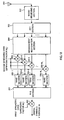
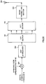
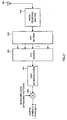
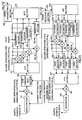
- FIG.23 is a block diagram showing the configuration of a radio communication apparatus according to Embodiment 5 of the present invention. Parts in FIG.23 identical to those in Embodiment 2 (FIG.10 and FIG.11) are assigned the same codes as in FIG.10 or FIG.11 and their detailed explanations are omitted.
- the radio communication apparatus shown in FIG.23 is a radio communication apparatus used in an FDD communication system.
- a communicating partner radio communication apparatus that communicates with this radio communication apparatus also has the same configuration.
- the transmitting side comprises, in addition to the configuration shown in FIG.10, a multiplexer 701, chip thinning-out section 702, and insertion sections 703-1 through 703-M 1
- the receiving side comprises, in addition to the configuration shown in FIG.11, channel estimators 704-1 through 704-M 1 and a separator 705.
- OFDM symbols from a communicating partner received at the receiving side undergo FFT processing by the FFT section 203, followed by input to channel estimators 704-1 through 704-M 1 for each subcarrier component.
- channel estimators 704-1 through 704-M 1 the channel quality of each subcarrier is estimated using a pilot signal inserted in each subcarrier. Pilot signals for performing channel estimation are pilot signals of fixed power inserted by insertion sections 703-1 through 703-M 1 on the communicating partner's transmitting side.
- a value (for example, amplitude fluctuation or phase fluctuation) indicating the channel quality of the receive channel estimated by channel estimators 704-1 through 704-M 1 is input to the multiplexer 701.
- channel estimation information is multiplexed on digital symbols.
- channel estimation information for each subcarrier transmitted from a communicating partner is separated by the separator 705, and input to the chip thinning-out section 702.
- the chip thinning-out section 702 the chip components of subcarriers with poor channel quality are thinned out in accordance with this channel estimation information for the transmit channel. That is, of the chips output from frequency domain spreader 301, chip components assigned to subcarriers whose amplitude fluctuation or phase fluctuation is equal to or greater than a predetermined threshold value are thinned out. Therefore, a signal is not transmitted on a subcarrier with poor channel quality.
- OFDM symbols are generated without assigning a chip component to a subcarrier with poor channel quality in an FDD communication system. That is to say, a signal is not transmitted on a subcarrier with poor channel quality.
- interference with other users can be reduced when a plurality of users' signals are code division multiplexed on each subcarrier.
- OFDM symbols are generated without assigning a chip component to a subcarrier with poor channel quality in a TDD (Time Division Duplex) communication system.
- TDD Time Division Duplex
- FIG.24 is a block diagram showing the configuration of a radio communication apparatus according to Embodiment 6 of the present invention. Parts in FIG.24 identical to those in Embodiment 5 (FIG.23) are assigned the same codes as in FIG.23 and their detailed explanations are omitted.
- the radio communication apparatus shown in FIG.24 is a radio communication apparatus used in a TDD communication system.
- a communicating party radio communication apparatus that communicates with this radio communication apparatus also has the same configuration.
- antenna 802 and radio transmitting section 105 are connected at the time of time-slot transmission
- antenna 802 and radio receiving section 202 are connected at the time of time-slot reception.
- TDD method unlike the FDD method, signals are transmitted and received using the same frequency band on the transmit channel and receive channel. Consequently, if the time slot interval is sufficiently short and channel conditions scarcely vary in adjacent transmission and reception times, channel quality estimated on the receiving side can be used as transmitting side channel quality.
- a value (for example, amplitude fluctuation or phase fluctuation) indicating the channel quality estimated by channel estimators 704-1 through 704-M 1 is input to a chip thinning-out section 702 as channel estimation information.
- the chip thinning-out section 702 the chip components of subcarriers with poor channel quality are thinned out using this channel estimation information for the receive channel as channel estimation information for the transmit channel. That is, of the chips output from frequency domain spreader 301, chip components assigned to subcarriers whose amplitude fluctuation or phase fluctuation is equal to or greater than a predetermined threshold value are thinned out. Therefore, a signal is not transmitted on a subcarrier with poor channel quality.
- Embodiment 5 the same effect as in Embodiment 5 can be obtained in a TDD communication system. That is to say, interference with other users can be reduced when a plurality of users' signals are code division multiplexed on each subcarrier. Also, as in Embodiment 5, although transmission characteristics are somewhat degraded by the thinning-out of chip components, this can be adequately compensated for by means of error correcting codes, etc.
- Embodiments 5 and 6 can also be implemented by being combined with any one of Embodiments 1 through 4.
- Embodiments 1 through 6 descriptions have been given taking the OFDM modulation method as an example of a multicarrier modulation method, but the present invention can be implemented with any multicarrier modulation method.
- the present invention is applicable to a communication terminal apparatus and base station apparatus used in a digital communication system.
Landscapes
- Engineering & Computer Science (AREA)
- Signal Processing (AREA)
- Computer Networks & Wireless Communication (AREA)
- Mobile Radio Communication Systems (AREA)
- Radio Relay Systems (AREA)
- Radar Systems Or Details Thereof (AREA)
Applications Claiming Priority (5)
| Application Number | Priority Date | Filing Date | Title |
|---|---|---|---|
| JP2000076904 | 2000-03-17 | ||
| JP2000076904 | 2000-03-17 | ||
| JP2000308884 | 2000-10-10 | ||
| JP2000308884 | 2000-10-10 | ||
| PCT/JP2001/002144 WO2001069826A1 (en) | 2000-03-17 | 2001-03-19 | Radio communication apparatus and radio communication method |
Publications (2)
| Publication Number | Publication Date |
|---|---|
| EP1179904A1 true EP1179904A1 (de) | 2002-02-13 |
| EP1179904A4 EP1179904A4 (de) | 2006-09-27 |
Family
ID=26587856
Family Applications (1)
| Application Number | Title | Priority Date | Filing Date |
|---|---|---|---|
| EP01914174A Withdrawn EP1179904A4 (de) | 2000-03-17 | 2001-03-19 | Verfahren und vorrichtung zur radio nachrichtenübertragung |
Country Status (6)
| Country | Link |
|---|---|
| US (1) | US20020159425A1 (de) |
| EP (1) | EP1179904A4 (de) |
| KR (1) | KR100454519B1 (de) |
| CN (1) | CN1364358A (de) |
| AU (1) | AU3954201A (de) |
| WO (1) | WO2001069826A1 (de) |
Cited By (10)
| Publication number | Priority date | Publication date | Assignee | Title |
|---|---|---|---|---|
| WO2003005617A1 (en) | 2001-07-05 | 2003-01-16 | Matsushita Electric Industrial Co., Ltd. | Radio communication apparatus and radio communication method |
| WO2004008681A1 (en) * | 2002-07-17 | 2004-01-22 | Koninklijke Philips Electronics N.V. | Time-frequency interleaved mc-cdma for quasi-synchronous systems |
| EP1432168A1 (de) * | 2002-12-16 | 2004-06-23 | Urmet Sistemi S.p.a. | Mehrträger CDMA Übertragungsverfahren mittels Hadamard Zeit-Frequenz Spreizkodes, sowie Sender und Empfänger für dieses Verfahren |
| EP1524793A1 (de) * | 2003-10-16 | 2005-04-20 | Mitsubishi Electric Information Technology Centre Europe B.V. | Verfahren zum Mapping von den Chips eines gespreitzten Symboles zu Unterkanälen von einem Mehrträgerübertragungsystem |
| WO2005062517A1 (en) * | 2003-12-19 | 2005-07-07 | Mitsubishi Denki Kabushiki Kaisha | Method and transmitter for communicating ultra wide bandwidth signals using orthogonal frequency division multiplexing modulation |
| GB2411550A (en) * | 2004-02-27 | 2005-08-31 | Toshiba Res Europ Ltd | Time domain spreading in a multiple-input multiple-output communications system |
| EP1408642A3 (de) * | 2002-10-09 | 2006-11-29 | NTT DoCoMo, Inc. | Adaptive Zuweisung für Mehrträgerspreizspektrumübertragung |
| EP1750387A1 (de) * | 2005-08-02 | 2007-02-07 | Samsung Electronics Co.,Ltd. | Verfahren zur zweidimensionalen Spreizung für ein OFDM-CDM-System |
| CN101141179B (zh) * | 2006-09-08 | 2011-06-01 | 华为技术有限公司 | 在无线通信系统中实现信息传递的方法及装置 |
| EP1617583A4 (de) * | 2003-04-24 | 2011-06-01 | Nec Corp | Funksende-/-empfangsvorrichtung und funksende-/-empfangsverfahren zur schützung der rausch- und st rungsleistung bei der verhültnis bertragung unter verwendung von codespreizung |
Families Citing this family (36)
| Publication number | Priority date | Publication date | Assignee | Title |
|---|---|---|---|---|
| US7787514B2 (en) * | 1998-02-12 | 2010-08-31 | Lot 41 Acquisition Foundation, Llc | Carrier interferometry coding with applications to cellular and local area networks |
| JP2001320342A (ja) * | 2000-05-11 | 2001-11-16 | Nec Corp | Fdm−cdma送信方法、fdm−cdma受信方法及びそれらの装置 |
| US7339955B2 (en) * | 2000-09-25 | 2008-03-04 | Pulse-Link, Inc. | TDMA communication method and apparatus using cyclic spreading codes |
| US7035201B2 (en) * | 2001-04-20 | 2006-04-25 | Mediatek Inc. | Programmable transceiver structure of multi-rate OFDM-CDMA for wireless multimedia communications |
| JP3396815B2 (ja) * | 2001-06-20 | 2003-04-14 | 富士通株式会社 | データ伝送方法及びデータ伝送装置 |
| JP3628987B2 (ja) * | 2001-07-31 | 2005-03-16 | 松下電器産業株式会社 | 無線通信装置および無線通信方法 |
| EP1436929B1 (de) * | 2001-10-19 | 2005-07-20 | Matsushita Electric Industrial Co., Ltd. | Vorrichtung und verfahren zur spreizspektrumübertragung |
| JP3727283B2 (ja) * | 2001-11-26 | 2005-12-14 | 松下電器産業株式会社 | 無線送信装置、無線受信装置及び無線送信方法 |
| US7450637B2 (en) | 2001-12-06 | 2008-11-11 | Pulse-Link, Inc. | Ultra-wideband communication apparatus and methods |
| US7483483B2 (en) | 2001-12-06 | 2009-01-27 | Pulse-Link, Inc. | Ultra-wideband communication apparatus and methods |
| US7406647B2 (en) | 2001-12-06 | 2008-07-29 | Pulse-Link, Inc. | Systems and methods for forward error correction in a wireless communication network |
| US7403576B2 (en) | 2001-12-06 | 2008-07-22 | Pulse-Link, Inc. | Systems and methods for receiving data in a wireless communication network |
| US8045935B2 (en) | 2001-12-06 | 2011-10-25 | Pulse-Link, Inc. | High data rate transmitter and receiver |
| US7391815B2 (en) | 2001-12-06 | 2008-06-24 | Pulse-Link, Inc. | Systems and methods to recover bandwidth in a communication system |
| US7317756B2 (en) | 2001-12-06 | 2008-01-08 | Pulse-Link, Inc. | Ultra-wideband communication apparatus and methods |
| CN100596044C (zh) | 2002-01-10 | 2010-03-24 | 富士通株式会社 | Ofdm系统中的导频复用方法和ofdm接收方法 |
| KR100457188B1 (ko) | 2002-10-07 | 2004-11-16 | 한국전자통신연구원 | 확산 방식 전환이 가능한 적응형 다중반송파코드분할다중접속 장치 및 그 방법 |
| US20050175073A1 (en) * | 2002-11-01 | 2005-08-11 | Kari Pajukoski | Data transmission method and transmitter |
| JP4163942B2 (ja) * | 2002-12-25 | 2008-10-08 | 松下電器産業株式会社 | 無線通信装置及び無線送信方法 |
| US7302238B2 (en) * | 2003-04-25 | 2007-11-27 | Samsung Electronics Co., Ltd. | Transmit diversity system, method and computer program product |
| JP3847733B2 (ja) | 2003-06-12 | 2006-11-22 | 松下電器産業株式会社 | マルチキャリア通信方法及びその通信装置 |
| JP2005057429A (ja) * | 2003-08-01 | 2005-03-03 | Nec Corp | Cdma通信装置およびその方法 |
| CN1833386B (zh) * | 2003-08-19 | 2011-04-06 | 松下电器产业株式会社 | 无线发送装置以及无线发送方法 |
| EP2058972B1 (de) * | 2003-12-25 | 2011-08-17 | NTT DoCoMo, Inc. | Funkkommunikationssystem, Sender, Empfänger und Funkkommunikationsverfahren |
| TWI253625B (en) * | 2004-04-06 | 2006-04-21 | I-Shun Huang | Signal-processing system and method thereof |
| CN1965522A (zh) * | 2004-06-10 | 2007-05-16 | 皇家飞利浦电子股份有限公司 | 通过至少两个信道同时发送信号 |
| JP4384667B2 (ja) * | 2004-06-24 | 2009-12-16 | パナソニック株式会社 | 無線送信装置および無線通信方法 |
| EP1655918A3 (de) * | 2004-11-03 | 2012-11-21 | Broadcom Corporation | Modus mit niedriger Rate und hoher Reichweite für OFDM in drahtlosen LANs |
| US7817744B2 (en) * | 2004-12-03 | 2010-10-19 | Panasonic Corporation | Wireless communication apparatus and data multiplexing method |
| CN102307074B (zh) * | 2004-12-14 | 2014-05-07 | 富士通株式会社 | 通信系统 |
| CN101099311B (zh) | 2005-01-13 | 2012-12-19 | 富士通株式会社 | 无线通信系统及方法 |
| JPWO2006114932A1 (ja) * | 2005-04-18 | 2008-12-11 | シャープ株式会社 | 無線通信装置および無線通信方法 |
| WO2006137708A1 (en) * | 2005-06-22 | 2006-12-28 | Samsung Electronics Co., Ltd. | Method and transmission apparatus for allocating resources to transmit uplink packet data in an orthogonal frequency division multiplexing system |
| JP4356702B2 (ja) * | 2006-03-03 | 2009-11-04 | ソニー株式会社 | 無線通信装置及び無線通信方法 |
| ES2373240T3 (es) | 2007-12-20 | 2012-02-01 | Panasonic Corporation | Señalización de canal de control usando un campo de señalización común para el formato de transporte y la versión de redundancia. |
| US8509325B2 (en) * | 2008-07-01 | 2013-08-13 | Qualcomm Incorporated | Adaptive thresholding for OFDM channel estimation |
Family Cites Families (7)
| Publication number | Priority date | Publication date | Assignee | Title |
|---|---|---|---|---|
| FR2701178A1 (fr) * | 1993-02-03 | 1994-08-05 | Philips Electronique Lab | Système de communication par étalement de spectre à multiutilisateurs. |
| EP2302808B1 (de) * | 1995-02-01 | 2013-06-05 | Sony Corporation | Mehrkanalübertragung mit Verschachtelung durch in-place Adressierung eines RAM-Speichers |
| JPH08331095A (ja) * | 1995-05-31 | 1996-12-13 | Sony Corp | 通信システム |
| SE504577C2 (sv) * | 1996-02-16 | 1997-03-10 | Ericsson Telefon Ab L M | Metod och anordning för kanaltilldelning i ett radiokommunikationssystem |
| DE19647833B4 (de) * | 1996-11-19 | 2005-07-07 | Deutsches Zentrum für Luft- und Raumfahrt e.V. | Verfahren zur gleichzeitigen Funkübertragung digitaler Daten zwischen mehreren Teilnehmerstationen und einer Basisstation |
| US6810030B1 (en) * | 1997-10-17 | 2004-10-26 | Lucent Technology | Dynamic and smart spreading for wideband CDMA |
| JP3236273B2 (ja) * | 1999-05-17 | 2001-12-10 | 三菱電機株式会社 | マルチキャリア伝送システムおよびマルチキャリア変調方法 |
-
2001
- 2001-03-19 US US09/979,022 patent/US20020159425A1/en not_active Abandoned
- 2001-03-19 AU AU39542/01A patent/AU3954201A/en not_active Abandoned
- 2001-03-19 WO PCT/JP2001/002144 patent/WO2001069826A1/ja not_active Ceased
- 2001-03-19 KR KR10-2001-7014591A patent/KR100454519B1/ko not_active Expired - Lifetime
- 2001-03-19 EP EP01914174A patent/EP1179904A4/de not_active Withdrawn
- 2001-03-19 CN CN01800537A patent/CN1364358A/zh active Pending
Cited By (16)
| Publication number | Priority date | Publication date | Assignee | Title |
|---|---|---|---|---|
| US7839759B2 (en) * | 2001-07-05 | 2010-11-23 | Panasonic Corporation | Radio communication apparatus and radio communication method |
| WO2003005617A1 (en) | 2001-07-05 | 2003-01-16 | Matsushita Electric Industrial Co., Ltd. | Radio communication apparatus and radio communication method |
| EP1347588A4 (de) * | 2001-07-05 | 2010-01-06 | Panasonic Corp | Funkkommunikationsvorrichtung und funkkommunikationsverfahren |
| WO2004008681A1 (en) * | 2002-07-17 | 2004-01-22 | Koninklijke Philips Electronics N.V. | Time-frequency interleaved mc-cdma for quasi-synchronous systems |
| US7606196B2 (en) | 2002-10-09 | 2009-10-20 | Ntt Docomo, Inc. | Radio communication system, radio communication method, and transmitter apparatus and receiver apparatus suitable for use in the same |
| EP1408642A3 (de) * | 2002-10-09 | 2006-11-29 | NTT DoCoMo, Inc. | Adaptive Zuweisung für Mehrträgerspreizspektrumübertragung |
| EP1432168A1 (de) * | 2002-12-16 | 2004-06-23 | Urmet Sistemi S.p.a. | Mehrträger CDMA Übertragungsverfahren mittels Hadamard Zeit-Frequenz Spreizkodes, sowie Sender und Empfänger für dieses Verfahren |
| EP1617583A4 (de) * | 2003-04-24 | 2011-06-01 | Nec Corp | Funksende-/-empfangsvorrichtung und funksende-/-empfangsverfahren zur schützung der rausch- und st rungsleistung bei der verhültnis bertragung unter verwendung von codespreizung |
| EP1524793A1 (de) * | 2003-10-16 | 2005-04-20 | Mitsubishi Electric Information Technology Centre Europe B.V. | Verfahren zum Mapping von den Chips eines gespreitzten Symboles zu Unterkanälen von einem Mehrträgerübertragungsystem |
| US7424009B2 (en) | 2003-10-16 | 2008-09-09 | Mitsubishi Denki Kabushiki Kaisha | Method of mapping chips of a spread out symbol to sub-channels of a multi-carrier transmission network |
| CN1720687B (zh) * | 2003-12-19 | 2010-08-25 | 三菱电机株式会社 | 用于使用正交频分复用调制通信超宽带宽信号的方法和发射机 |
| WO2005062517A1 (en) * | 2003-12-19 | 2005-07-07 | Mitsubishi Denki Kabushiki Kaisha | Method and transmitter for communicating ultra wide bandwidth signals using orthogonal frequency division multiplexing modulation |
| GB2411550B (en) * | 2004-02-27 | 2006-07-12 | Toshiba Res Europ Ltd | Communications system, method and device |
| GB2411550A (en) * | 2004-02-27 | 2005-08-31 | Toshiba Res Europ Ltd | Time domain spreading in a multiple-input multiple-output communications system |
| EP1750387A1 (de) * | 2005-08-02 | 2007-02-07 | Samsung Electronics Co.,Ltd. | Verfahren zur zweidimensionalen Spreizung für ein OFDM-CDM-System |
| CN101141179B (zh) * | 2006-09-08 | 2011-06-01 | 华为技术有限公司 | 在无线通信系统中实现信息传递的方法及装置 |
Also Published As
| Publication number | Publication date |
|---|---|
| EP1179904A4 (de) | 2006-09-27 |
| AU3954201A (en) | 2001-09-24 |
| US20020159425A1 (en) | 2002-10-31 |
| CN1364358A (zh) | 2002-08-14 |
| KR20020000176A (ko) | 2002-01-04 |
| WO2001069826A1 (en) | 2001-09-20 |
| KR100454519B1 (ko) | 2004-11-05 |
Similar Documents
| Publication | Publication Date | Title |
|---|---|---|
| EP1179904A1 (de) | Verfahren und vorrichtung zur radio nachrichtenübertragung | |
| US8363632B2 (en) | Radio transmitting apparatus, radio receiving apparatus, and radio transmission method | |
| KR101176321B1 (ko) | E?utran을 위한 이차 동기 코드북 | |
| US9106356B2 (en) | Radio communication device and radio communication method | |
| US7616608B2 (en) | OFDM-CDMA transmission device and OFDM-CDMA transmission method | |
| KR20000008080A (ko) | 부호분할다중접속 통신시스템의 부호간섭 제거장치 및 방법 | |
| KR20050043297A (ko) | 다중 안테나를 사용하는 직교주파수분할다중 시스템에서간섭신호 제거 장치 및 방법 | |
| JP2002190788A (ja) | 無線通信装置および無線通信方法 | |
| EP0922350B1 (de) | Vermittlungssystem mit diversität in einer orthogonalen frequenzmultiplexumgebung, und betriebsverfahren | |
| JP4731055B2 (ja) | 無線通信装置及び無線通信方法 | |
| AU711458B2 (en) | Multipath resistant, orthogonal code-division multiple access system | |
| Tan et al. | Multi-rate access schemes for MC-CDMA | |
| KR20050062973A (ko) | 부호 분할 다중 이동통신 시스템에서 주파수 영역 등화장치 및 방법 | |
| Kim et al. | Impact of the antenna array on the uplink synchronous orthogonal multicarrier DS-CDMA RAKE system in dispersive fading channels | |
| Gu et al. | UCHT complex sequences for downlink multi-carrier DS-CDMA systems | |
| Sreesudha | MIMOMIMO MIMO-CDMA TechnologiesCDMA Technologies CDMA TechnologiesCDMA Technologies CDMA TechnologiesCDMA Technologies CDMA TechnologiesCDMA Technologies CDMA Technologies CDMA Technologies CDMA | |
| Sandhya | A Study on Similarity Join in Heterogeneous Information Network Using Path Based Algorithm | |
| CN101662353A (zh) | 发送装置、方法、通信终端装置和基站装置 |
Legal Events
| Date | Code | Title | Description |
|---|---|---|---|
| PUAI | Public reference made under article 153(3) epc to a published international application that has entered the european phase |
Free format text: ORIGINAL CODE: 0009012 |
|
| 17P | Request for examination filed |
Effective date: 20011207 |
|
| AK | Designated contracting states |
Kind code of ref document: A1 Designated state(s): AT BE CH CY DE DK ES FI FR GB GR IE IT LI LU MC NL PT SE TR |
|
| AX | Request for extension of the european patent |
Free format text: AL;LT;LV;MK;RO;SI |
|
| RBV | Designated contracting states (corrected) |
Designated state(s): DE FR GB |
|
| A4 | Supplementary search report drawn up and despatched |
Effective date: 20060828 |
|
| 17Q | First examination report despatched |
Effective date: 20070216 |
|
| STAA | Information on the status of an ep patent application or granted ep patent |
Free format text: STATUS: THE APPLICATION IS DEEMED TO BE WITHDRAWN |
|
| 18D | Application deemed to be withdrawn |
Effective date: 20070627 |