EP1180802A2 - Dispositif photovoltaique amélioré à plasmon de surface - Google Patents
Dispositif photovoltaique amélioré à plasmon de surface Download PDFInfo
- Publication number
- EP1180802A2 EP1180802A2 EP01115030A EP01115030A EP1180802A2 EP 1180802 A2 EP1180802 A2 EP 1180802A2 EP 01115030 A EP01115030 A EP 01115030A EP 01115030 A EP01115030 A EP 01115030A EP 1180802 A2 EP1180802 A2 EP 1180802A2
- Authority
- EP
- European Patent Office
- Prior art keywords
- electrode
- spheres
- array
- apertures
- metallic
- Prior art date
- Legal status (The legal status is an assumption and is not a legal conclusion. Google has not performed a legal analysis and makes no representation as to the accuracy of the status listed.)
- Withdrawn
Links
Images


Classifications
-
- H—ELECTRICITY
- H10—SEMICONDUCTOR DEVICES; ELECTRIC SOLID-STATE DEVICES NOT OTHERWISE PROVIDED FOR
- H10F—INORGANIC SEMICONDUCTOR DEVICES SENSITIVE TO INFRARED RADIATION, LIGHT, ELECTROMAGNETIC RADIATION OF SHORTER WAVELENGTH OR CORPUSCULAR RADIATION
- H10F77/00—Constructional details of devices covered by this subclass
- H10F77/10—Semiconductor bodies
- H10F77/14—Shape of semiconductor bodies; Shapes, relative sizes or dispositions of semiconductor regions within semiconductor bodies
- H10F77/148—Shapes of potential barriers
-
- H—ELECTRICITY
- H10—SEMICONDUCTOR DEVICES; ELECTRIC SOLID-STATE DEVICES NOT OTHERWISE PROVIDED FOR
- H10F—INORGANIC SEMICONDUCTOR DEVICES SENSITIVE TO INFRARED RADIATION, LIGHT, ELECTROMAGNETIC RADIATION OF SHORTER WAVELENGTH OR CORPUSCULAR RADIATION
- H10F19/00—Integrated devices, or assemblies of multiple devices, comprising at least one photovoltaic cell covered by group H10F10/00, e.g. photovoltaic modules
- H10F19/20—Integrated devices, or assemblies of multiple devices, comprising at least one photovoltaic cell covered by group H10F10/00, e.g. photovoltaic modules comprising photovoltaic cells in arrays in or on a single semiconductor substrate, the photovoltaic cells having planar junctions
-
- H—ELECTRICITY
- H10—SEMICONDUCTOR DEVICES; ELECTRIC SOLID-STATE DEVICES NOT OTHERWISE PROVIDED FOR
- H10F—INORGANIC SEMICONDUCTOR DEVICES SENSITIVE TO INFRARED RADIATION, LIGHT, ELECTROMAGNETIC RADIATION OF SHORTER WAVELENGTH OR CORPUSCULAR RADIATION
- H10F19/00—Integrated devices, or assemblies of multiple devices, comprising at least one photovoltaic cell covered by group H10F10/00, e.g. photovoltaic modules
- H10F19/90—Structures for connecting between photovoltaic cells, e.g. interconnections or insulating spacers
- H10F19/902—Structures for connecting between photovoltaic cells, e.g. interconnections or insulating spacers for series or parallel connection of photovoltaic cells
- H10F19/904—Structures for connecting between photovoltaic cells, e.g. interconnections or insulating spacers for series or parallel connection of photovoltaic cells characterised by the shapes of the structures
-
- H—ELECTRICITY
- H10—SEMICONDUCTOR DEVICES; ELECTRIC SOLID-STATE DEVICES NOT OTHERWISE PROVIDED FOR
- H10F—INORGANIC SEMICONDUCTOR DEVICES SENSITIVE TO INFRARED RADIATION, LIGHT, ELECTROMAGNETIC RADIATION OF SHORTER WAVELENGTH OR CORPUSCULAR RADIATION
- H10F77/00—Constructional details of devices covered by this subclass
- H10F77/10—Semiconductor bodies
- H10F77/14—Shape of semiconductor bodies; Shapes, relative sizes or dispositions of semiconductor regions within semiconductor bodies
- H10F77/147—Shapes of bodies
-
- H—ELECTRICITY
- H10—SEMICONDUCTOR DEVICES; ELECTRIC SOLID-STATE DEVICES NOT OTHERWISE PROVIDED FOR
- H10F—INORGANIC SEMICONDUCTOR DEVICES SENSITIVE TO INFRARED RADIATION, LIGHT, ELECTROMAGNETIC RADIATION OF SHORTER WAVELENGTH OR CORPUSCULAR RADIATION
- H10F77/00—Constructional details of devices covered by this subclass
- H10F77/20—Electrodes
- H10F77/206—Electrodes for devices having potential barriers
- H10F77/211—Electrodes for devices having potential barriers for photovoltaic cells
-
- Y—GENERAL TAGGING OF NEW TECHNOLOGICAL DEVELOPMENTS; GENERAL TAGGING OF CROSS-SECTIONAL TECHNOLOGIES SPANNING OVER SEVERAL SECTIONS OF THE IPC; TECHNICAL SUBJECTS COVERED BY FORMER USPC CROSS-REFERENCE ART COLLECTIONS [XRACs] AND DIGESTS
- Y02—TECHNOLOGIES OR APPLICATIONS FOR MITIGATION OR ADAPTATION AGAINST CLIMATE CHANGE
- Y02E—REDUCTION OF GREENHOUSE GAS [GHG] EMISSIONS, RELATED TO ENERGY GENERATION, TRANSMISSION OR DISTRIBUTION
- Y02E10/00—Energy generation through renewable energy sources
- Y02E10/50—Photovoltaic [PV] energy
Definitions
- the present invention relates generally to photovoltaic devices and, more particularly, to flexible and stretchable photovoltaic devices with surface-plasmon enhanced conversion efficiency.
- PV photovoltaic
- PV modules are made on crystalline silicon wafers. It is straightforward to fabricate a planar p-n junction by growing various layers with the required dopants, and to pattern the front current collecting electrode, usually in a fingered geometry. While a planar geometry is useful for such flat-area applications as rooftop solar panels, in some cases it is preferable to have PV devices which are flexible, or which can be fabricated on a curved surface, for instance to act as a functional electricity generating "skin" on portable devices such as laptops or cellular phones, or even car roofs and hoods, without giving up design aesthetics.
- amorphous semiconductors which can be evaporated onto a flexible plastic substrate, as is disclosed in U.S. Patents 4,663,828 and 4,663,829, to R.A. Hartman and P.E. Koch, respectively.
- a flexible device proposed by Texas Instruments Inc. is known as a Spheral device and is disclosed in U.S. Patent 4,614,835 to K.R. Carson et al. The total yield of these Spheral devices is claimed to be close to 10%, which if accurate is impressive for devices that are not made of single-crystal silicon.
- Spheral devices have semiconductor spheres lodged in apertures in a perforated metal electrode and are sandwiched between the perforated metal electrode and a second electrode.
- the spheres are comprised of an n-doped semiconductor and a p-doped semiconductor with one contacting the perforated metal electrode and the other contacting the second electrode. While these devices have a degree of flexibility, they are not stretchable and do not have a degree of flexibility needed to conform to the shape of surfaces used in many electrical devices.
- a surface plasmon enhanced photovoltaic device and method for its fabrication are provided.
- the surface plasmon enhanced photovoltaic device boosts the performance of commercially available photovoltaic devices such as those based on Texas Instruments Spheral technology in which the current-generating p-n junction is between two layers or shells of a silicon sphere.
- Spheres are lodged in a large array in apertures of a metallic front electrode of which the surface topography is such that incident (sun)light interacts resonantly with surface plasmons on the metal surface. This leads to an enhancement of the oscillating electric fields, and therefore of the effective light intensity, at the spheres. Since the overall device can be designed to be mechanically flexible, it may be applied as a power-generating skin to a device to be powered.
- the surface-plasmon enhanced photovoltaic device of the present invention comprises: a first metallic electrode having an array of apertures, the first metallic electrode having an illuminated surface upon which light is incident and an unilluminated surface, at least one of the illuminated and unilluminated surfaces having an enhancement characteristic resulting in a resonant interaction of the incident light with surface plasmons on the surface; a second electrode spaced from the first metallic electrode; and a plurality of spheres corresponding to the array of apertures and disposed between the first metallic and second electrodes, each sphere having a first portion of either p or n-doped material and a second portion having the other of the p or n-doped material such that a p-n junction is formed at a junction between the first and second portions, an individual sphere being disposed in the apertures such that one of the first or second portions is in electrical contact with the first metallic electrode and the other of the first or second portions is in electrical contact with the second electrode.
- the enhancement characteristic preferably comprises a periodic surface topography, such as holes, dimples, or surface corrugations, on at least one of the illuminated and unilluminated surfaces of the first metallic electrode, the apertures in the metallic electrode being of a diameter comparable to or less than a wavelength of light incident thereon.
- the first portion is an outer portion or shell and the second portion is a center portion or core of the spheres where the shell is in electrical contact with the first metallic electrode and the core is in electrical contact with the second electrode.
- an electrical device comprising: at least one component requiring a power supply; and a power supply for powering the at least one component.
- the power supply comprises the surface-plasmon enhanced photovoltaic device of the present invention.
- the surface-plasmon enhanced photovoltaic device further comprises an under layer fixed to the second electrode and a pressure sensitive adhesive backing on a free surface of the under layer for applying the surface-plasmon enhanced photovoltaic device to an exterior surface of the electrical device.
- the photovoltaic device comprises: a first metallic electrode having an array of apertures; a second electrode spaced from the first metallic electrode; and a plurality of PV spheres corresponding to the array of apertures and disposed between the first metallic and second electrodes, each PV sphere having a shell of either p or n-doped material and a core having the other of the p or n-doped material such that a p-n junction is formed at a junction between the shell and core, an individual sphere being disposed in the apertures such that the shell is in electrical contact with the first metallic electrode and the core is in electrical contact with the second electrode.
- the method comprises the steps of: providing the first metallic electrode having the array of apertures; providing an array of the PV spheres, each PV sphere corresponding to an aperture in the first metallic electrode; depositing a photo resist on the shells; developing the photo resist to expose a portion of the shells; etching the exposed portion of the shells to expose a corresponding portion of the core; and depositing the second electrode on the exposed core.
- the providing of the first metallic electrode having an array of apertures preferably comprises the sub-steps of: providing a substrate; forming a periodic array of first polymer spheres on the substrate; etching the first polymer spheres to form an array of etched polymer spheres, the etched polymer spheres being smaller than the first polymer spheres and having the same lattice constant; depositing a conductive film on the substrate and array of etched polymer spheres; and removing the array of etched polymer spheres resulting in the first metallic electrode being carried on the substrate.
- the PV spheres are preferably fixed to the first metallic electrode with an adhesive to fill any gaps between the spheres in which case any adhesive from what will become the exposed portion of the shells must be removed. Furthermore, the etching step of the PV spheres preferably results in an overhang of the photo resist such that depositing the second electrode allows electrical contact to the core of the PV sphere while preventing electrical contact of the shell with the second electrode.
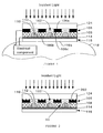
- the photovoltaic device 100 has a plurality of spheres 102, preferably Si, lodged into an array of apertures 104 in a first metallic electrode 106 (alternatively referred to herein as the first electrode), preferably a metal foil.
- the spheres are preferably held in place by an adhesive 108.
- a first portion 110 of the spheres 102 is doped with a type of dopant (n or p) opposite to that of a second portion 112, so that a p-n junction is formed at the interface between the first and second portions 110, 112, respectively.
- the first portion 110 is an outer shell or portion and the second portion is a center core or portion of the spheres 102.
- the invention will be described in such environment. However, those of skill in the art will recognize that any number of configurations or materials can be utilized without departing from the scope or spirit of the invention.
- An alternative configuration may be where the PV sphere comprises two semi-spherical portions.
- the outer portion 110 makes electrical contact with the first electrode 106 in which the spheres 102 are lodged.
- An opposite side of the spheres is processed to expose the center portion 112, so that the center portion 112 makes electrical contact with a second electrode 114.
- An insulating under layer 116 is preferably provided which serves to protect the second electrode 114 and may be provided with a pressure sensitive adhesive backing 116a. Light incident on the spheres 102 through the apertures 104 in the first electrode 106 generates a photo current which flows between the first and second electrodes 106 and 114, respectively.
- the photovoltaic device 100 of the present invention is significantly improved over those known in the art in several ways.
- One such improvement is to use much smaller spheres 102, with diameters on the order of 1 ⁇ m. This allows the fabrication of photovoltaic devices with far greater mechanical flexibility than the Spheral devices of the prior art which have sphere diameters on the order of 1 mm, and makes possible a slight stretching of the substrate which may be useful in those cases in which the photovoltaic device needs to be molded around the contours of the hardware to be powered.
- a portable electrical device 118 which has at least one component 120 requiring electrical power.
- the overall efficiency of the PV device can be improved significantly by the use of a surface plasmon enhanced device (PED) as the first electrode.
- PED surface plasmon enhanced device
- the conversion efficiency of the Spheral device of the prior art is limited by the total area of the apertures 104 in the first electrode 106.
- the photovoltaic device 100 of the present invention boosts the total efficiency of the photovoltaic devices of the prior art significantly, without expanding the fractional area of the apertures 104 which would compromise the mechanical strength and the electrical reliability of the device, by using a resonance of the incident light with surface plasmons on either an illuminated surface 106a of the first electrode 106 upon which light is incident, or an unilluminated surface 106b, or both.
- the effect of the interaction with the surface plasmons is to concentrate the light at the apertures 104, which is where the photovoltaic spheres 102 are lodged, thus boosting the conversion efficiency per unit incident flux.
- the optical transmission is expected to be very small, and to be proportional to the fourth power of the ratio of the aperture diameter and the optical wavelength: T ⁇ (d/ ⁇ ) 4 .
- the metal is perforated with an array of such subwavelength apertures, the optical transmission is enhanced by several orders of magnitude, and the total transmission can in fact exceed the fractional area occupied by the apertures.
- the enhancement is a result of a resonant interaction of the incident light with surface plasmons (electronic excitations which are confined to the metal surface).
- the periodic structure of the aperture array allows grating coupling of the surface plasmons and the exciting light, through the grating momentum.
- the resulting band diagram can be probed by measuring the transmission as a function of incident angle; high transmission is obtained when both energy and momentum conservation are satisfied.
- the zero-order transmission spectra also show extinctions, or deep minima. These are due to Wood's anomaly, which occurs in diffraction gratings when a diffracted order becomes tangent to the plane of the grating. [See H.F. Ghaemi et al., Phys. Rev. B 58, 6779 (1998)].
- the periodic structure on the first electrode 106 need not be an array of apertures 104, any surface topology will give rise to the transmission enhancement, such as a periodic array of indentations or dimples 202 on either the top surface (illuminated surface 106a) or bottom surface (unilluminated surface 106b) of electrode 106.
- the transmission through a single aperture is boosted significantly by the presence of a dimple array on either surface of the first electrode, compared to the transmission of an aperture in a smooth film.
- the wavelength at which the enhancement occurs can be tuned, since it is determined by the lattice constant of the dimple array [See D.E. Grupp et al., Adv. Mater. 11, 860 (1999)].
- a mini-array of 7 holes (a tiny part of a hexagonal array) is sufficient to get the full transmission enhancement of a large hexagonal array, albeit that the spectral features are broad.
- the total transmission of the light scales with the total aperture area and is independent of the wavelength, while a single aperture in a smooth metal film has a transmission which scales as (d/ ⁇ ) 4 . So the relative transmission enhancement is most pronounced for small apertures and long wavelength. [See T. Thio et al., JOSA B, 16, 1743 (1999)].
- the total amount of light emerging from the apertures can be as large as twice the light directly incident on the apertures, even if the aperture is smaller than the wavelength of the light. Furthermore, calculations show that the oscillating electric field is enhanced in and near the apertures by factors >10 compared with the fields associated with the incident radiation, this corresponds to a boost in the intensity of more than two orders of magnitude, exactly at the places where the photocurrent generating spheres are located.
- the action of the surface plasmon enhanced device compensates for the loss of surface area due to the finite area occupied by the apertures in the perforated first electrode 106, and enhances significantly the overall conversion efficiency of the photovoltaic device 100.
- the first electrode 106 serves as an electrode with high parallelism so that the effect of defective photovoltaic spheres is minimized.
- the transmission spectrum of the first electrode 106 can be matched to the response spectrum of the photovoltaic device, since the transmission spectrum of the first electrode 106 has a set of peaks of which the center wavelength is determined by the lattice constant of the aperture array, and with a width determined by both the aperture size and the optical properties of the metal used for the first electrode 106.
- Preferable materials for optimizing the performance of the spheres 102 are II-VI or III-V semiconductors, many of which have band gaps in the visible range, matching the broad maximum of the solar spectrum.
- silicon is also a viable material, indeed most of the solar cells in commercial production now use silicon.
- Fabricating semiconductor spheres 102 at this length scale is a challenge because the spheres 102 are too small to obtain by mechanical grinding methods and too large for assembly by chemical means.
- a first alternative is to start with a sphere, preferably metallic, which is slightly smaller than the desired size, and then coating it with two layers of semiconductor such that the semiconductors form a p-n junction at their interface.
- a preferable way to achieve this is by chemical deposition from a solution.
- a second alternative-is to use larger semiconductor spheres, with diameter ⁇ 5 ⁇ m, also with a p-n junction, and optimizing the surface plasmon enhanced transmission by fabricating a surface pattern as discussed above, such as corrugations or dimples 202 with the appropriate periodicity, preferably close to P 600nm.
- the width of the transmission peaks depends on the optical properties of the first electrode 106, but only that portion of the first electrode 106 which is within a skin depth of the surface 106a, 106b. It is, after all, the surface plasmons which mediate the transmission enhancement.
- the surface layers 106a, 106b re made of silver, which in the visible region exhibits surface-plasmon enhanced transmission peaks with a narrow width and high transmission maxima, and thus high electric field enhancement near and in the apertures.
- the total throughput can be increased significantly by matching the refractive indices of the dielectric media (124, 108) on the two sides (106a, 106b) of the perforated first electrode 106 in the presence of identical surface corrugation on both surfaces, as discussed more fully in co-pending U.S. Application serial no. 09/435,132 filed November 5, 1999, which is incorporated herein by its reference.
- the resulting coincidence of the surface plasmon dispersion relation on the two surfaces leads to a resonant enhancement of the already large transmission. This process may be understood in terms of a resonant tunneling through the apertures 104 in the first electrode 106.
- the resonance condition is met when the index of refraction of a first dielectric (alternatively referred to as over layer 124) is substantially equal to the effective refractive index of the composite medium consisting of the semiconductor spheres 102 and a second dielectric which is in direct contact with the first electrode 106.
- This second dielectric may be the adhesive 108 which fixes the spheres 102 in their position, or may be a thin dielectric layer 106c overcoating the bottom side of the perforated first electrode 106. In the latter case the thickness of the dielectric layer 106c must be at least as large as the skin depth of the surface plasmon mode, typically 100-200nm.
- self-assembly is the preferred method to create the array of apertures 104 in the first electrode 106, as well as to lodge the semiconductor spheres 102 in the apertures 104. Both can be done by using dispersions of spheres in a suitable liquid. Techniques for obtaining large areas of two-dimensional arrays of spheres are well known in the art. These techniques rely on a large effective attraction between the particles on the surface of the substrate, through surface tension of the liquid, and therefore always give rise to hexagonal close-packed structures, which have the additional advantage of large intensity enhancement compared to, other arrays such as a square array [Tineke Thio, H.F. Ghaemi, H.J. Lezec, P.A. Wolff, and T.W. Ebbesen, J. Opt. Soc. Am. B. 16 , 1743 (1999)].
- the outer portion 110 of the spheres 102 must be mechanically fixed to the first electrode 106 in such a way as to ensure ohmic contact with the first electrode 106. This may be done by the uniform deposition (e.g. by sputtering) of a suitable insulator 108 (which may also be an adhesive as discussed above) such as PMMA. Then a separate electrical contact must be made from the center portion 112 of the spheres 102 to the second electrode 114. In the large-diameter Spheral devices of the prior art this is done by mechanical polishing, but this is not practical in the case of micron-sized spheres.
- the two materials comprising the p-n junctions can be chemically dissimilar so that the etching rates are sufficiently different to etch only the outer portion 110 but not the center portion 112.
- a combination of a III-V and a II-VI semiconductor is one possibility.
- a final metallization provides the second electrode 114.
- the second electrode 114 may be covered by the protective overlayer 116 of polymer or other insulator.
- Figures 3a-3e and 4a-4e illustrate a preferred process for fabricating the perforated first electrode 106 [Haginoya, C.; Ishibashi, A.M.; Koike, K., Applied Physics Letters, 71, 2934-6, (1997)] while Figures 4a-4e illustrate a preferred process for fabricating the remaining components of the photovoltaic device 100 of the present invention.
- a substrate 124 (which will become the over layer) is first provided, which may be flexible if desired.
- a two-dimensional array of polymer spheres 302 is formed by crystallization from an aqueous suspension, as shown in Figure 3b.
- Such a crystallization method relies on the strong attraction between the spheres 302 due to surface tension effects, and results in a well-ordered hexagonal lattice of spheres 302, with a lattice constant equal to the diameter of the spheres 302. There will be occasional defects such as vacancies, and dislocations, which will alter locally the symmetry of the lattice.
- the transmission enhancement is sensitive to the local environment only within 2-3 lattice constants, so as long as such defects occur at a low enough density (their spacing is more than 5-10 lattice constants), they do not contribute significantly to the total optical transmission through the perforated first electrode 106. In this case the transmission enhancement close to the defects will simply be smaller than at the locations with perfect crystallinity, but will also not affect the overall device performance significantly.
- the next step in the process involves dry etching of the polymer spheres 302, preferably by using a reactive ion etch with an oxygen plasma. This reduces the diameter of each sphere, without changing their locations, resulting in an ordered array of smaller spheres 302a with the same lattice constant as the original array.
- a metal film 304 is then deposited, preferably, by thermal or E-beam evaporation as is shown in Figure 3d. After removal of the spheres 304, preferably by dissolving in acetone, the end result is a metal film perforated with apertures 104 located in a periodic hexagonal array as shown in Figure 3e. The perforated metal film serves as the first electrode 106.
- FIG. 4a-4e the formation of the plurality of spheres 102 and their connectivity with the first and second electrodes 106, 114 are discussed.
- On top of the first electrode 106 is grown an array of the semiconductor spheres 102 with p-n junctions as shown in Figure 4a.
- the diameter of these spheres may be equal to the lattice constant of the aperture array in the first electrode 106, or may be an integer multiple thereof, in which case apertures will also lie in between spheres as shown in Figure 4a.
- These spheres are crystallized by self-assembly using the same method as that outlined above, but the substrate now has indentations at the locations of the apertures 104, which fixes the position (the phase) of the semiconductor sphere array.
- the diameters of the semiconductor spheres 102 and that of the original polymer spheres 302 should be commensurate (that is, their ratio should be a rational number, and preferably an integer).
- the spheres 102 are fixed to the first electrode 106 with the adhesive 108 which is preferably clear and conducting, in order to allow the incident light to reach the spheres 102, to make good electrical contact to the first electrode 106, and to each other.
- the adhesive 108 is dissolved in the colloidal suspension for good penetration between the spheres 102 and the first electrode 106. Any adhesive 108 which is left on top of the spheres 102 is then removed, preferably by a dry etch to expose a portion 402 of the spheres 102.
- a photo resist 404 having non-linear properties is then deposited onto the sphere 102 array.
- the light When exposed to ultra-violet light, the light is concentrated near the tops of the semiconductor spheres (because of their high refractive index), and developing the photo resist will result in apertures 406 in the photo resist 404 located near the tops of the spheres as shown in Figure 4c.
- the diameter of these apertures 406 depends on the exact materials parameters of the photo resist 404 and the exposure parameters.
- an additional layer of Cr may be used (on top of the photo resist 404) to act as an etch mask for the next step, should the photo resist 404 by itself be insufficient to act as an effective mask.
- the next step is an etch of the outer portion 110 of the spheres 102.
- the etch may be dry or wet and preferably results in an undercut 408, or an overhang of the photo resist etch mask 404a.
- the purpose of the undercut 408 is to prevent electrical contact of the outer portion 110 with the second electrode 114, which is to be deposited by an angle-selective process such as E-beam or thermal evaporation as shown in Figure 4e.
- a polymer layer 116 may be applied on top of the second electrode 114 which may include an adhesive layer 116a to fix the photovoltaic device to a rigid substrate (such as in the case of rooftop applications), or the electrical device 118 to be powered (such as in the case of a portable device).
- the dielectric layers i.e., the over and under layers 124, 116, respectively
- the entire structure of which the total thickness can be as small as 10 ⁇ m, can be made flexible and could even be designed such that it remains operational under some amount of stretch.
- the proper mechanical properties of the over layer 124 can also contribute greatly to the ruggedness of the device, so that it is practical to use it as a power generating skin which is not too delicate and can withstand a degree of abuse.
- Such an integration of the power generation onto the electrical device 118 to be powered would open the door to truly portable computing and telecommunication.
Landscapes
- Photovoltaic Devices (AREA)
Applications Claiming Priority (2)
| Application Number | Priority Date | Filing Date | Title |
|---|---|---|---|
| US09/638,686 US6441298B1 (en) | 2000-08-15 | 2000-08-15 | Surface-plasmon enhanced photovoltaic device |
| US638686 | 2000-08-15 |
Publications (2)
| Publication Number | Publication Date |
|---|---|
| EP1180802A2 true EP1180802A2 (fr) | 2002-02-20 |
| EP1180802A3 EP1180802A3 (fr) | 2012-02-29 |
Family
ID=24561013
Family Applications (1)
| Application Number | Title | Priority Date | Filing Date |
|---|---|---|---|
| EP01115030A Withdrawn EP1180802A3 (fr) | 2000-08-15 | 2001-06-20 | Dispositif photovoltaique amélioré à plasmon de surface |
Country Status (3)
| Country | Link |
|---|---|
| US (1) | US6441298B1 (fr) |
| EP (1) | EP1180802A3 (fr) |
| JP (1) | JP3726887B2 (fr) |
Cited By (11)
| Publication number | Priority date | Publication date | Assignee | Title |
|---|---|---|---|---|
| WO2011061011A3 (fr) * | 2009-11-18 | 2012-02-02 | International Business Machines Corporation | Grilles d'électrode perforées pour cellules photovoltaïques à dimensions caractéristiques infra-longueur d'onde et supra-longueur d'onde |
| WO2012143859A1 (fr) | 2011-04-19 | 2012-10-26 | Gerardino Annamaria | Dispositif de production d'énergie électrique à partir de sources de chaleur |
| EP2478290A4 (fr) * | 2009-09-15 | 2014-01-15 | Nthdegree Tech Worldwide Inc | Appareil et système d'émission de lumière, photovoltaïque ou électronique et leur procédé de fabrication |
| EP2430653A4 (fr) * | 2009-05-08 | 2014-09-03 | 1366 Tech Inc | Couche de décollement poreuse permettant le retrait sélectif de films déposés sur des surfaces |
| EP2720280A4 (fr) * | 2011-06-10 | 2015-03-04 | Jx Nippon Oil & Energy Corp | Élément de conversion photoélectrique |
| US9200758B2 (en) | 2007-05-31 | 2015-12-01 | Nthdegree Technologies Worldwide Inc | LED lighting apparatus formed by a printable composition of a liquid or gel suspension of diodes and methods of using same |
| US9343593B2 (en) | 2007-05-31 | 2016-05-17 | Nthdegree Technologies Worldwide Inc | Printable composition of a liquid or gel suspension of diodes |
| US9349928B2 (en) | 2007-05-31 | 2016-05-24 | Nthdegree Technologies Worldwide Inc | Method of manufacturing a printable composition of a liquid or gel suspension of diodes |
| US9362348B2 (en) | 2007-05-31 | 2016-06-07 | Nthdegree Technologies Worldwide Inc | Method of manufacturing a light emitting, power generating or other electronic apparatus |
| US9419179B2 (en) | 2007-05-31 | 2016-08-16 | Nthdegree Technologies Worldwide Inc | Diode for a printable composition |
| US9534772B2 (en) | 2007-05-31 | 2017-01-03 | Nthdegree Technologies Worldwide Inc | Apparatus with light emitting diodes |
Families Citing this family (124)
| Publication number | Priority date | Publication date | Assignee | Title |
|---|---|---|---|---|
| US9607301B2 (en) * | 2000-04-27 | 2017-03-28 | Merck Patent Gmbh | Photovoltaic sensor facilities in a home environment |
| US20050268962A1 (en) * | 2000-04-27 | 2005-12-08 | Russell Gaudiana | Flexible Photovoltaic cells, systems and methods |
| US20050257827A1 (en) * | 2000-04-27 | 2005-11-24 | Russell Gaudiana | Rotational photovoltaic cells, systems and methods |
| US20060076048A1 (en) * | 2000-04-27 | 2006-04-13 | Russell Gaudiana | Photo-sensing photovoltaic with positioning facility |
| US20060005876A1 (en) * | 2000-04-27 | 2006-01-12 | Russell Gaudiana | Mobile photovoltaic communication facilities |
| US6818907B2 (en) * | 2000-10-17 | 2004-11-16 | The President And Fellows Of Harvard College | Surface plasmon enhanced illumination system |
| US6563041B2 (en) * | 2000-11-29 | 2003-05-13 | Kyocera Corporation | Photoelectric conversion device |
| US6653552B2 (en) * | 2001-02-28 | 2003-11-25 | Kyocera Corporation | Photoelectric conversion device and method of manufacturing the same |
| GB0217900D0 (en) * | 2002-08-02 | 2002-09-11 | Qinetiq Ltd | Optoelectronic devices |
| US20060137734A1 (en) * | 2002-11-20 | 2006-06-29 | Mortenson Mark G | High efficiency solar cells |
| US7170142B2 (en) * | 2003-10-03 | 2007-01-30 | Applied Materials, Inc. | Planar integrated circuit including a plasmon waveguide-fed Schottky barrier detector and transistors connected therewith |
| WO2005057247A2 (fr) * | 2003-12-05 | 2005-06-23 | University Of Pittsburgh | Lentilles metalliques nano-optiques et dispositifs de mise en forme de faisceau |
| KR100682887B1 (ko) | 2004-01-30 | 2007-02-15 | 삼성전자주식회사 | 나노구조 형성방법 |
| WO2005092037A2 (fr) * | 2004-03-22 | 2005-10-06 | Research Foundation Of The City University Of New York | Dispositif optoelectronique metal-semiconducteur-metal a bande passante et responsivite elevees |
| CN1965414B (zh) | 2004-04-05 | 2010-09-29 | 日本电气株式会社 | 光电二极管及其制造方法 |
| US7110154B2 (en) * | 2004-06-10 | 2006-09-19 | Clemson University | Plasmon-photon coupled optical devices |
| US7626179B2 (en) | 2005-09-30 | 2009-12-01 | Virgin Island Microsystems, Inc. | Electron beam induced resonance |
| US7586097B2 (en) | 2006-01-05 | 2009-09-08 | Virgin Islands Microsystems, Inc. | Switching micro-resonant structures using at least one director |
| US7791290B2 (en) | 2005-09-30 | 2010-09-07 | Virgin Islands Microsystems, Inc. | Ultra-small resonating charged particle beam modulator |
| WO2006130164A2 (fr) | 2004-08-19 | 2006-12-07 | University Of Pittsburgh | Analyseurs de spectre optiques, de la dimension d'une puce, a resolution accrue |
| US7302129B2 (en) * | 2004-10-12 | 2007-11-27 | Lockheed Martin Corporation | Optical transistor with sub-wavelength aperture |
| WO2007064358A2 (fr) | 2005-09-30 | 2007-06-07 | Virgin Islands Microsystems, Inc. | Structures et methodes de couplage de l'energie d'une onde electromagnetique |
| US7579609B2 (en) | 2005-12-14 | 2009-08-25 | Virgin Islands Microsystems, Inc. | Coupling light of light emitting resonator to waveguide |
| US7470920B2 (en) | 2006-01-05 | 2008-12-30 | Virgin Islands Microsystems, Inc. | Resonant structure-based display |
| US7619373B2 (en) | 2006-01-05 | 2009-11-17 | Virgin Islands Microsystems, Inc. | Selectable frequency light emitter |
| JP2007225767A (ja) * | 2006-02-22 | 2007-09-06 | Nec Corp | 受光装置 |
| US7443358B2 (en) * | 2006-02-28 | 2008-10-28 | Virgin Island Microsystems, Inc. | Integrated filter in antenna-based detector |
| US20070200071A1 (en) * | 2006-02-28 | 2007-08-30 | Virgin Islands Microsystems, Inc. | Coupling output from a micro resonator to a plasmon transmission line |
| US7605835B2 (en) | 2006-02-28 | 2009-10-20 | Virgin Islands Microsystems, Inc. | Electro-photographic devices incorporating ultra-small resonant structures |
| EP1995793A4 (fr) | 2006-03-13 | 2017-07-05 | NEC Corporation | Photodiode, procede de fabrication d'une telle photodiode, dispositif de communication optique et module d'interconnexion optique |
| US7558490B2 (en) | 2006-04-10 | 2009-07-07 | Virgin Islands Microsystems, Inc. | Resonant detector for optical signals |
| US7492868B2 (en) | 2006-04-26 | 2009-02-17 | Virgin Islands Microsystems, Inc. | Source of x-rays |
| US7646991B2 (en) | 2006-04-26 | 2010-01-12 | Virgin Island Microsystems, Inc. | Selectable frequency EMR emitter |
| US7876793B2 (en) | 2006-04-26 | 2011-01-25 | Virgin Islands Microsystems, Inc. | Micro free electron laser (FEL) |
| US8188431B2 (en) | 2006-05-05 | 2012-05-29 | Jonathan Gorrell | Integration of vacuum microelectronic device with integrated circuit |
| US7732786B2 (en) | 2006-05-05 | 2010-06-08 | Virgin Islands Microsystems, Inc. | Coupling energy in a plasmon wave to an electron beam |
| US7442940B2 (en) * | 2006-05-05 | 2008-10-28 | Virgin Island Microsystems, Inc. | Focal plane array incorporating ultra-small resonant structures |
| US7746532B2 (en) | 2006-05-05 | 2010-06-29 | Virgin Island Microsystems, Inc. | Electro-optical switching system and method |
| US7741934B2 (en) | 2006-05-05 | 2010-06-22 | Virgin Islands Microsystems, Inc. | Coupling a signal through a window |
| US7342441B2 (en) * | 2006-05-05 | 2008-03-11 | Virgin Islands Microsystems, Inc. | Heterodyne receiver array using resonant structures |
| US7554083B2 (en) | 2006-05-05 | 2009-06-30 | Virgin Islands Microsystems, Inc. | Integration of electromagnetic detector on integrated chip |
| US7723698B2 (en) | 2006-05-05 | 2010-05-25 | Virgin Islands Microsystems, Inc. | Top metal layer shield for ultra-small resonant structures |
| US7718977B2 (en) * | 2006-05-05 | 2010-05-18 | Virgin Island Microsystems, Inc. | Stray charged particle removal device |
| US7557647B2 (en) | 2006-05-05 | 2009-07-07 | Virgin Islands Microsystems, Inc. | Heterodyne receiver using resonant structures |
| US7476907B2 (en) * | 2006-05-05 | 2009-01-13 | Virgin Island Microsystems, Inc. | Plated multi-faceted reflector |
| US7728397B2 (en) | 2006-05-05 | 2010-06-01 | Virgin Islands Microsystems, Inc. | Coupled nano-resonating energy emitting structures |
| US7583370B2 (en) | 2006-05-05 | 2009-09-01 | Virgin Islands Microsystems, Inc. | Resonant structures and methods for encoding signals into surface plasmons |
| US7443577B2 (en) * | 2006-05-05 | 2008-10-28 | Virgin Islands Microsystems, Inc. | Reflecting filtering cover |
| US20070258492A1 (en) * | 2006-05-05 | 2007-11-08 | Virgin Islands Microsystems, Inc. | Light-emitting resonant structure driving raman laser |
| US7569836B2 (en) | 2006-05-05 | 2009-08-04 | Virgin Islands Microsystems, Inc. | Transmission of data between microchips using a particle beam |
| US7986113B2 (en) | 2006-05-05 | 2011-07-26 | Virgin Islands Microsystems, Inc. | Selectable frequency light emitter |
| US7710040B2 (en) | 2006-05-05 | 2010-05-04 | Virgin Islands Microsystems, Inc. | Single layer construction for ultra small devices |
| US7359589B2 (en) * | 2006-05-05 | 2008-04-15 | Virgin Islands Microsystems, Inc. | Coupling electromagnetic wave through microcircuit |
| US7436177B2 (en) | 2006-05-05 | 2008-10-14 | Virgin Islands Microsystems, Inc. | SEM test apparatus |
| US7586167B2 (en) * | 2006-05-05 | 2009-09-08 | Virgin Islands Microsystems, Inc. | Detecting plasmons using a metallurgical junction |
| US7728702B2 (en) | 2006-05-05 | 2010-06-01 | Virgin Islands Microsystems, Inc. | Shielding of integrated circuit package with high-permeability magnetic material |
| US7656094B2 (en) | 2006-05-05 | 2010-02-02 | Virgin Islands Microsystems, Inc. | Electron accelerator for ultra-small resonant structures |
| JP4772585B2 (ja) * | 2006-05-10 | 2011-09-14 | 浜松ホトニクス株式会社 | 光検出器 |
| US7573045B2 (en) | 2006-05-15 | 2009-08-11 | Virgin Islands Microsystems, Inc. | Plasmon wave propagation devices and methods |
| US7679067B2 (en) | 2006-05-26 | 2010-03-16 | Virgin Island Microsystems, Inc. | Receiver array using shared electron beam |
| US8866007B2 (en) | 2006-06-07 | 2014-10-21 | California Institute Of Technology | Plasmonic photovoltaics |
| US7655934B2 (en) | 2006-06-28 | 2010-02-02 | Virgin Island Microsystems, Inc. | Data on light bulb |
| US8482197B2 (en) * | 2006-07-05 | 2013-07-09 | Hamamatsu Photonics K.K. | Photocathode, electron tube, field assist type photocathode, field assist type photocathode array, and field assist type electron tube |
| JP5000216B2 (ja) * | 2006-07-05 | 2012-08-15 | 浜松ホトニクス株式会社 | 光電陰極および電子管 |
| GB0614891D0 (en) * | 2006-07-27 | 2006-09-06 | Univ Southampton | Plasmon-enhanced photo voltaic cell |
| US7450794B2 (en) * | 2006-09-19 | 2008-11-11 | Virgin Islands Microsystems, Inc. | Microcircuit using electromagnetic wave routing |
| US7560716B2 (en) | 2006-09-22 | 2009-07-14 | Virgin Islands Microsystems, Inc. | Free electron oscillator |
| US20110043918A1 (en) * | 2006-12-08 | 2011-02-24 | David Thomas Crouse | Devices and methods for light control in material composites |
| US20100200941A1 (en) | 2006-12-20 | 2010-08-12 | Junichi Fujikata | Photodiode, optical communication device, and optical interconnection module |
| US7659513B2 (en) | 2006-12-20 | 2010-02-09 | Virgin Islands Microsystems, Inc. | Low terahertz source and detector |
| WO2008136479A1 (fr) | 2007-05-01 | 2008-11-13 | Nec Corporation | Photodiode de type à couplage de chemin de guide d'onde |
| US7990336B2 (en) | 2007-06-19 | 2011-08-02 | Virgin Islands Microsystems, Inc. | Microwave coupled excitation of solid state resonant arrays |
| US7791053B2 (en) | 2007-10-10 | 2010-09-07 | Virgin Islands Microsystems, Inc. | Depressed anode with plasmon-enabled devices such as ultra-small resonant structures |
| EP2269101A4 (fr) * | 2007-12-10 | 2013-01-09 | Univ City New York Res Found | Procedes, dispositifs et structures a sous-longueur d'onde de regulation de lumiere dans des materiaux composites |
| JP5170110B2 (ja) | 2008-01-10 | 2013-03-27 | 日本電気株式会社 | 半導体受光素子及び光通信デバイス |
| JP5628690B2 (ja) * | 2008-02-29 | 2014-11-19 | アイメックImec | 導電性ナノシェルの作製 |
| JP5475246B2 (ja) * | 2008-03-24 | 2014-04-16 | 株式会社東芝 | 太陽電池 |
| WO2010005622A2 (fr) * | 2008-06-16 | 2010-01-14 | Konarka Technologies, Inc. | Dispositifs télescopiques |
| US8802965B2 (en) * | 2008-09-19 | 2014-08-12 | Regents Of The University Of Minnesota | Plasmonic nanocavity devices and methods for enhanced efficiency in organic photovoltaic cells |
| CN102187425B (zh) * | 2008-10-16 | 2013-11-06 | 小利兰·斯坦福大学托管委员会 | 光子增强型热离子发射 |
| TWI383176B (zh) * | 2008-10-20 | 2013-01-21 | Univ Nat Chiao Tung | 兆赫波分束器裝置 |
| KR20110102322A (ko) * | 2008-12-10 | 2011-09-16 | 가부시키가이샤 시나노 | 박막 광전 변환 소자와 박막 광전 변환 소자의 제조 방법 |
| US20110247690A1 (en) * | 2008-12-17 | 2011-10-13 | David Thomas Crouse | Semiconductor devices comprising antireflective conductive layers and methods of making and using |
| US20100224236A1 (en) * | 2009-03-03 | 2010-09-09 | Alliance For Sustainable Energy, Llc | Nanohole Film Electrodes |
| US20100229943A1 (en) * | 2009-03-16 | 2010-09-16 | Lightwave Power, Inc. | Asymmetric Waveguide |
| JP5667748B2 (ja) * | 2009-03-18 | 2015-02-12 | 株式会社東芝 | 光透過型太陽電池およびその製造方法 |
| JP2010219407A (ja) * | 2009-03-18 | 2010-09-30 | Toshiba Corp | メッシュ構造を有する電極を具備した太陽電池及びその製造方法 |
| JP5562568B2 (ja) * | 2009-03-18 | 2014-07-30 | 株式会社東芝 | ショットキー型太陽電池及び製造方法 |
| JP5667747B2 (ja) * | 2009-03-18 | 2015-02-12 | 株式会社東芝 | 薄膜太陽電池およびその製造方法 |
| JP5135269B2 (ja) * | 2009-03-18 | 2013-02-06 | 株式会社東芝 | 太陽電池とその製造方法 |
| US8097402B2 (en) * | 2009-03-31 | 2012-01-17 | Tokyo Electron Limited | Using electric-field directed post-exposure bake for double-patterning (D-P) |
| WO2010118418A2 (fr) * | 2009-04-10 | 2010-10-14 | Lightwave Power, Inc. | Dispositif plasmonique plan pour réflexion, diffusion et guidage de lumière |
| US8809672B2 (en) * | 2009-05-27 | 2014-08-19 | The Regents Of The University Of California | Nanoneedle plasmonic photodetectors and solar cells |
| EP2453484A4 (fr) | 2009-07-06 | 2013-12-04 | Toyota Motor Co Ltd | Élément de conversion photoélectrique |
| US8866000B2 (en) * | 2009-07-31 | 2014-10-21 | Corey A. Weiss | Ultra-efficient energy conversion device for converting light to electricity by rectifying surface plasmon polaritons |
| US8106421B2 (en) * | 2009-08-21 | 2012-01-31 | University Of Seoul Industry Cooperation Foundation | Photovoltaic devices |
| GB0915687D0 (en) | 2009-09-08 | 2009-10-07 | Dupont Teijin Films Us Ltd | Polyester films |
| JP2011076774A (ja) * | 2009-09-29 | 2011-04-14 | Sony Corp | 発光装置および表示装置 |
| KR101649696B1 (ko) * | 2009-10-29 | 2016-08-22 | 엘지디스플레이 주식회사 | 프린지 필드형 액정표시장치 및 그 제조방법 |
| KR101338117B1 (ko) * | 2009-10-29 | 2013-12-06 | 엘지디스플레이 주식회사 | 액정표시장치 및 그 제조방법 |
| KR101640814B1 (ko) * | 2009-10-30 | 2016-07-20 | 엘지디스플레이 주식회사 | 표면 플라즈몬을 이용한 컬러필터 및 액정표시장치 |
| US8675279B2 (en) | 2009-12-15 | 2014-03-18 | Toyota Motor Engineering And Manufacturing North America, Inc. | Grating structure for dividing light |
| KR101272052B1 (ko) * | 2009-12-18 | 2013-06-05 | 엘지디스플레이 주식회사 | 표면 플라즈몬을 이용한 컬러필터 및 액정표시장치의 제조방법 |
| KR101313654B1 (ko) * | 2009-12-18 | 2013-10-02 | 엘지디스플레이 주식회사 | 표면 플라즈몬을 이용한 컬러필터와 액정표시장치 및 그 제조방법 |
| KR101274591B1 (ko) * | 2009-12-18 | 2013-06-13 | 엘지디스플레이 주식회사 | 표면 플라즈몬을 이용한 컬러필터와 액정표시장치 및 그 제조방법 |
| US20110226317A1 (en) * | 2010-03-22 | 2011-09-22 | Fang Xu | Surface Plasmon Resonance Enhanced Solar Cell Structure with Broad Spectral and Angular Bandwidth and Polarization Insensitivity |
| WO2011125101A1 (fr) * | 2010-04-02 | 2011-10-13 | 株式会社 東芝 | Elément convertisseur photoélectrique et procédé de fabrication associé |
| US8236604B2 (en) * | 2010-09-03 | 2012-08-07 | Tetrasun, Inc. | Fine line metallization of photovoltaic devices by partial lift-off of optical coatings |
| JP5398678B2 (ja) * | 2010-09-29 | 2014-01-29 | 株式会社東芝 | 光電変換素子 |
| CN102082186B (zh) * | 2010-10-29 | 2013-05-08 | 华南师范大学 | 电极及其制造方法 |
| US9893223B2 (en) | 2010-11-16 | 2018-02-13 | Suncore Photovoltaics, Inc. | Solar electricity generation system |
| JP5541137B2 (ja) * | 2010-12-15 | 2014-07-09 | ソニー株式会社 | 撮像装置、電子機器、太陽電池、および、撮像装置の製造方法 |
| GB2488787A (en) * | 2011-03-07 | 2012-09-12 | Dupont Teijin Films Us Ltd | Stabilised polyester films |
| KR101245160B1 (ko) * | 2011-05-02 | 2013-03-19 | 한국화학연구원 | 플라즈몬 공명을 이용한 유기박막 태양전지 및 그의 제조방법 |
| JP5713856B2 (ja) * | 2011-09-26 | 2015-05-07 | 株式会社東芝 | 光透過型金属電極、電子装置及び光学素子 |
| US20130118906A1 (en) * | 2011-11-16 | 2013-05-16 | University Of Southern California | Method and system for enhancing catalytic and photocatalytic processes |
| US9324966B2 (en) | 2013-03-15 | 2016-04-26 | E I Du Pont De Nemours And Company | Thin-film transparent conductive structure and devices made therewith |
| GB201310837D0 (en) | 2013-06-18 | 2013-07-31 | Dupont Teijin Films Us Ltd | Polyester film -IV |
| GB201317551D0 (en) | 2013-10-03 | 2013-11-20 | Dupont Teijin Films Us Ltd | Co-extruded polyester films |
| WO2015066446A1 (fr) * | 2013-11-01 | 2015-05-07 | Gentex Corporation | Module émetteur-récepteur capable d'apprentissage |
| US9929291B2 (en) | 2014-02-06 | 2018-03-27 | Raytheon Company | Photo-detector having plasmonic resonance and photon crystal thermal noise suppression |
| US9673341B2 (en) | 2015-05-08 | 2017-06-06 | Tetrasun, Inc. | Photovoltaic devices with fine-line metallization and methods for manufacture |
| CN106898663A (zh) * | 2017-02-23 | 2017-06-27 | 京东方科技集团股份有限公司 | 一种太阳能电池、太阳能电池的制作方法及用电设备 |
| US11737293B2 (en) | 2021-02-19 | 2023-08-22 | The Regents Of The University Of Michigan | Artificial photosynthetic devices utilizing polariton antennas |
Family Cites Families (42)
| Publication number | Priority date | Publication date | Assignee | Title |
|---|---|---|---|---|
| US3866037A (en) | 1957-11-22 | 1975-02-11 | American Optical Corp | Optical systems and associated detecting means |
| US3998659A (en) * | 1974-01-28 | 1976-12-21 | Texas Instruments Incorporated | Solar cell with semiconductor particles and method of fabrication |
| US4360273A (en) | 1980-02-14 | 1982-11-23 | Sperry Corporation | Optical alignment of masks for X-ray lithography |
| JPS57106031A (en) | 1980-12-23 | 1982-07-01 | Toshiba Corp | Transferring device for fine pattern |
| US4405238A (en) | 1981-05-20 | 1983-09-20 | Ibm Corporation | Alignment method and apparatus for x-ray or optical lithography |
| US4521640A (en) * | 1981-09-08 | 1985-06-04 | Texas Instruments Incorporated | Large area, low temperature process, fault tolerant solar energy converter |
| US4407320A (en) * | 1981-09-08 | 1983-10-04 | Texas Instruments Incorporated | Large area, fault tolerant solar energy converter |
| US4554727A (en) * | 1982-08-04 | 1985-11-26 | Exxon Research & Engineering Company | Method for making optically enhanced thin film photovoltaic device using lithography defined random surfaces |
| US4556790A (en) | 1982-11-30 | 1985-12-03 | At&T Bell Laboratories | Photodetector having a contoured, substantially periodic surface |
| US4555622A (en) * | 1982-11-30 | 1985-11-26 | At&T Bell Laboratories | Photodetector having semi-insulating material and a contoured, substantially periodic surface |
| US4482778A (en) * | 1983-04-19 | 1984-11-13 | The United States Of America As Represented By The Administrator Of The National Aeronautics And Space Administration | Solar energy converter using surface plasma waves |
| US4659429A (en) | 1983-08-03 | 1987-04-21 | Cornell Research Foundation, Inc. | Method and apparatus for production and use of nanometer scale light beams |
| US4662747A (en) | 1983-08-03 | 1987-05-05 | Cornell Research Foundation, Inc. | Method and apparatus for production and use of nanometer scale light beams |
| US4614835A (en) | 1983-12-15 | 1986-09-30 | Texas Instruments Incorporated | Photovoltaic solar arrays using silicon microparticles |
| US4957601A (en) * | 1984-09-04 | 1990-09-18 | Texas Instruments Incorporated | Method of forming an array of apertures in an aluminum foil |
| US4582588A (en) * | 1984-09-04 | 1986-04-15 | Texas Instruments Incorporated | Method of anodizing and sealing aluminum |
| US4663828A (en) | 1985-10-11 | 1987-05-12 | Energy Conversion Devices, Inc. | Process and apparatus for continuous production of lightweight arrays of photovoltaic cells |
| US4663829A (en) | 1985-10-11 | 1987-05-12 | Energy Conversion Devices, Inc. | Process and apparatus for continuous production of lightweight arrays of photovoltaic cells |
| US4891830A (en) | 1986-03-28 | 1990-01-02 | Shimadzu Corporation | X-ray reflective mask and system for image formation with use of the same |
| US4815854A (en) | 1987-01-19 | 1989-03-28 | Nec Corporation | Method of alignment between mask and semiconductor wafer |
| US5028546A (en) * | 1989-07-31 | 1991-07-02 | Texas Instruments Incorporated | Method for manufacture of solar cell with foil contact point |
| US5091319A (en) * | 1989-07-31 | 1992-02-25 | Hotchkiss Gregory B | Method of affixing silicon spheres to a foil matrix |
| JP2609953B2 (ja) * | 1991-03-08 | 1997-05-14 | 理化学研究所 | 表面プラズモン顕微鏡 |
| US5250812A (en) | 1991-03-29 | 1993-10-05 | Hitachi, Ltd. | Electron beam lithography using an aperture having an array of repeated unit patterns |
| US5351127A (en) | 1992-06-17 | 1994-09-27 | Hewlett-Packard Company | Surface plasmon resonance measuring instruments |
| US5306902A (en) | 1992-09-01 | 1994-04-26 | International Business Machines Corporation | Confocal method and apparatus for focusing in projection lithography |
| US5354985A (en) | 1993-06-03 | 1994-10-11 | Stanford University | Near field scanning optical and force microscope including cantilever and optical waveguide |
| US5451980A (en) | 1993-10-19 | 1995-09-19 | The University Of Toledo | Liquid crystal flat panel color display with surface plasmon scattering |
| US5570139A (en) | 1994-05-13 | 1996-10-29 | Wang; Yu | Surface plasmon high efficiency HDTV projector |
| US5498576A (en) * | 1994-07-22 | 1996-03-12 | Texas Instruments Incorporated | Method and apparatus for affixing spheres to a foil matrix |
| US5486494A (en) * | 1994-07-22 | 1996-01-23 | Texas Instruments Incorporated | Method and apparatus for affixing spheres to a conductive sheet |
| US5510156A (en) * | 1994-08-23 | 1996-04-23 | Analog Devices, Inc. | Micromechanical structure with textured surface and method for making same |
| DE4438391C2 (de) | 1994-10-27 | 1997-07-03 | Evotec Biosystems Gmbh | Vorrichtung zur Bestimmung stoffspezifischer Parameter eines oder weniger Moleküle mittels Korrelations-Spektroskopie |
| US5663798A (en) | 1995-05-08 | 1997-09-02 | Dr. Khaled Karrai Und Dr. Miles Haines Gesellschaft Burgerlichen Rechts | Far-field characterization of sub-wavelength sized apertures |
| US5686919A (en) * | 1995-06-06 | 1997-11-11 | Jordan; James R. | Process for generating wind profiler data free of fixed ground clutter contamination |
| US5633972A (en) | 1995-11-29 | 1997-05-27 | Trustees Of Tufts College | Superresolution imaging fiber for subwavelength light energy generation and near-field optical microscopy |
| US5789742A (en) | 1996-10-28 | 1998-08-04 | Nec Research Institute, Inc. | Near-field scanning optical microscope probe exhibiting resonant plasmon excitation |
| US5846843A (en) | 1996-11-18 | 1998-12-08 | The University Of Toledo | Sensor using long range surface plasmon resonance with diffraction double-grating |
| JP3369439B2 (ja) * | 1997-06-05 | 2003-01-20 | 科学技術振興事業団 | 光応答電極および湿式太陽電池 |
| US5973316A (en) | 1997-07-08 | 1999-10-26 | Nec Research Institute, Inc. | Sub-wavelength aperture arrays with enhanced light transmission |
| US6040936A (en) | 1998-10-08 | 2000-03-21 | Nec Research Institute, Inc. | Optical transmission control apparatus utilizing metal films perforated with subwavelength-diameter holes |
| US6236033B1 (en) * | 1998-12-09 | 2001-05-22 | Nec Research Institute, Inc. | Enhanced optical transmission apparatus utilizing metal films having apertures and periodic surface topography |
-
2000
- 2000-08-15 US US09/638,686 patent/US6441298B1/en not_active Expired - Lifetime
-
2001
- 2001-06-20 EP EP01115030A patent/EP1180802A3/fr not_active Withdrawn
- 2001-07-16 JP JP2001215272A patent/JP3726887B2/ja not_active Expired - Fee Related
Cited By (17)
| Publication number | Priority date | Publication date | Assignee | Title |
|---|---|---|---|---|
| US9400086B2 (en) | 2007-05-31 | 2016-07-26 | Nthdegree Technologies Worldwide Inc | Apparatus with light emitting or absorbing diodes |
| US9410684B2 (en) | 2007-05-31 | 2016-08-09 | Nthdegree Technologies Worldwide Inc | Bidirectional lighting apparatus with light emitting diodes |
| US9777914B2 (en) | 2007-05-31 | 2017-10-03 | Nthdegree Technologies Worldwide Inc. | Light emitting apparatus having at least one reverse-biased light emitting diode |
| US9534772B2 (en) | 2007-05-31 | 2017-01-03 | Nthdegree Technologies Worldwide Inc | Apparatus with light emitting diodes |
| US9419179B2 (en) | 2007-05-31 | 2016-08-16 | Nthdegree Technologies Worldwide Inc | Diode for a printable composition |
| US9349928B2 (en) | 2007-05-31 | 2016-05-24 | Nthdegree Technologies Worldwide Inc | Method of manufacturing a printable composition of a liquid or gel suspension of diodes |
| US9362348B2 (en) | 2007-05-31 | 2016-06-07 | Nthdegree Technologies Worldwide Inc | Method of manufacturing a light emitting, power generating or other electronic apparatus |
| US9200758B2 (en) | 2007-05-31 | 2015-12-01 | Nthdegree Technologies Worldwide Inc | LED lighting apparatus formed by a printable composition of a liquid or gel suspension of diodes and methods of using same |
| US9316362B2 (en) | 2007-05-31 | 2016-04-19 | Nthdegree Technologies Worldwide Inc | LED lighting apparatus formed by a printable composition of a liquid or gel suspension of diodes and methods of using same |
| US9343593B2 (en) | 2007-05-31 | 2016-05-17 | Nthdegree Technologies Worldwide Inc | Printable composition of a liquid or gel suspension of diodes |
| TWI502759B (zh) * | 2009-05-08 | 2015-10-01 | 1366科技公司 | 用於選擇性移除沉積薄膜的多孔剝離層 |
| EP2430653A4 (fr) * | 2009-05-08 | 2014-09-03 | 1366 Tech Inc | Couche de décollement poreuse permettant le retrait sélectif de films déposés sur des surfaces |
| EP2478290A4 (fr) * | 2009-09-15 | 2014-01-15 | Nthdegree Tech Worldwide Inc | Appareil et système d'émission de lumière, photovoltaïque ou électronique et leur procédé de fabrication |
| US8120132B2 (en) | 2009-11-18 | 2012-02-21 | International Business Machines Corporation | Holey electrode grids for photovoltaic cells with subwavelength and superwavelength feature sizes |
| WO2011061011A3 (fr) * | 2009-11-18 | 2012-02-02 | International Business Machines Corporation | Grilles d'électrode perforées pour cellules photovoltaïques à dimensions caractéristiques infra-longueur d'onde et supra-longueur d'onde |
| WO2012143859A1 (fr) | 2011-04-19 | 2012-10-26 | Gerardino Annamaria | Dispositif de production d'énergie électrique à partir de sources de chaleur |
| EP2720280A4 (fr) * | 2011-06-10 | 2015-03-04 | Jx Nippon Oil & Energy Corp | Élément de conversion photoélectrique |
Also Published As
| Publication number | Publication date |
|---|---|
| JP2002076410A (ja) | 2002-03-15 |
| EP1180802A3 (fr) | 2012-02-29 |
| JP3726887B2 (ja) | 2005-12-14 |
| US6441298B1 (en) | 2002-08-27 |
Similar Documents
| Publication | Publication Date | Title |
|---|---|---|
| US6441298B1 (en) | Surface-plasmon enhanced photovoltaic device | |
| Massiot et al. | Progress and prospects for ultrathin solar cells | |
| US20140069496A1 (en) | Planar Plasmonic Device for Light Reflection, Diffusion and Guiding | |
| US8039292B2 (en) | Holey electrode grids for photovoltaic cells with subwavelength and superwavelength feature sizes | |
| US9263600B2 (en) | Silicon nanoparticle photovoltaic devices | |
| US20110162699A1 (en) | Solar cell with funnel-like groove structure | |
| CN102082186B (zh) | 电极及其制造方法 | |
| KR20010014686A (ko) | 박막 반도체 장치 및 그 제조 방법 | |
| KR20140095553A (ko) | 전자기 에너지 수집 장치, 시스템 및 방법 | |
| TW201320369A (zh) | 使用磊晶剝離之整合太陽能收集器及冷焊接合之半導體太陽能電池 | |
| KR101783971B1 (ko) | 금속 디스크 어레이를 구비한 적층형 태양전지 | |
| US20130014814A1 (en) | Nanostructured arrays for radiation capture structures | |
| Anderson et al. | Combined optical–electrical finite-element simulations of thin-film solar cells with homogeneous and nonhomogeneous intrinsic layers | |
| Aly et al. | Highly efficient SiO2 trapezoidal grating-based thin-film solar cell | |
| Cordaro et al. | Nanopatterned back-reflector with engineered near-field/far-field light scattering for enhanced light trapping in silicon-based multijunction solar cells | |
| Abdelraouf et al. | All dielectric and plasmonic cross-grating metasurface for efficient perovskite solar cells | |
| Mortazavifar et al. | Absorption improvement of a-Si/c-Si rectangular nanowire arrays in ultrathin solar cells | |
| US10658968B2 (en) | Near-field based thermoradiative device | |
| US20140209154A1 (en) | Embedded Nanopatterns for Optical Absorbance and Photovoltaics | |
| Seassal et al. | Photonic crystal assisted ultra-thin silicon photovoltaic solar cell | |
| Rezk et al. | Strong reduction in Ge film reflectivity by an overlayer of 3 nm Si nanoparticles: Implications for photovoltaics | |
| US10566475B2 (en) | High-efficiency photoelectric element and method for manufacturing same | |
| Vora | Increasing solar energy conversion efficiency in thin film hydrogenated amorphous silicon solar cells with patterned plasmonic silver nano-disk array | |
| Karaagac et al. | Synthesis of one-dimentional nanostructures for gas sensing and photovoltaic applications | |
| Yassin et al. | Design of step pyramidal nanoparticle for plasmonic photovoltaics |
Legal Events
| Date | Code | Title | Description |
|---|---|---|---|
| PUAI | Public reference made under article 153(3) epc to a published international application that has entered the european phase |
Free format text: ORIGINAL CODE: 0009012 |
|
| AK | Designated contracting states |
Kind code of ref document: A2 Designated state(s): AT BE CH CY DE DK ES FI FR GB GR IE IT LI LU MC NL PT SE TR |
|
| AX | Request for extension of the european patent |
Free format text: AL;LT;LV;MK;RO;SI |
|
| RAP1 | Party data changed (applicant data changed or rights of an application transferred) |
Owner name: NEC LABORATORIES AMERICA, INC. |
|
| PUAL | Search report despatched |
Free format text: ORIGINAL CODE: 0009013 |
|
| AK | Designated contracting states |
Kind code of ref document: A3 Designated state(s): AT BE CH CY DE DK ES FI FR GB GR IE IT LI LU MC NL PT SE TR |
|
| AX | Request for extension of the european patent |
Extension state: AL LT LV MK RO SI |
|
| RIC1 | Information provided on ipc code assigned before grant |
Ipc: H01L 31/05 20060101ALI20120126BHEP Ipc: H01L 31/0224 20060101ALI20120126BHEP Ipc: H01L 31/0236 20060101ALI20120126BHEP Ipc: H01L 31/042 20060101ALI20120126BHEP Ipc: H01L 31/0352 20060101AFI20120126BHEP |
|
| 17P | Request for examination filed |
Effective date: 20120829 |
|
| AKX | Designation fees paid |
Designated state(s): DE FR GB |
|
| STAA | Information on the status of an ep patent application or granted ep patent |
Free format text: STATUS: THE APPLICATION HAS BEEN WITHDRAWN |
|
| 18W | Application withdrawn |
Effective date: 20130711 |