EP1180911A2 - Format de trame optique - Google Patents
Format de trame optique Download PDFInfo
- Publication number
- EP1180911A2 EP1180911A2 EP01117080A EP01117080A EP1180911A2 EP 1180911 A2 EP1180911 A2 EP 1180911A2 EP 01117080 A EP01117080 A EP 01117080A EP 01117080 A EP01117080 A EP 01117080A EP 1180911 A2 EP1180911 A2 EP 1180911A2
- Authority
- EP
- European Patent Office
- Prior art keywords
- units
- stuff
- framing
- optical
- connect switch
- Prior art date
- Legal status (The legal status is an assumption and is not a legal conclusion. Google has not performed a legal analysis and makes no representation as to the accuracy of the status listed.)
- Withdrawn
Links
- 230000003287 optical effect Effects 0.000 title claims abstract description 51
- 238000009432 framing Methods 0.000 claims abstract description 63
- 238000004891 communication Methods 0.000 claims abstract description 20
- 239000011159 matrix material Substances 0.000 claims abstract description 20
- 230000007704 transition Effects 0.000 claims abstract description 11
- 238000000034 method Methods 0.000 claims description 13
- 239000013307 optical fiber Substances 0.000 claims description 5
- 238000012937 correction Methods 0.000 claims description 4
- 238000011084 recovery Methods 0.000 description 5
- 238000010586 diagram Methods 0.000 description 4
- 238000007689 inspection Methods 0.000 description 4
- 238000006243 chemical reaction Methods 0.000 description 3
- 238000001514 detection method Methods 0.000 description 2
- 238000011161 development Methods 0.000 description 2
- 239000000835 fiber Substances 0.000 description 2
- 230000003278 mimic effect Effects 0.000 description 2
- 238000012986 modification Methods 0.000 description 2
- 230000004048 modification Effects 0.000 description 2
- 238000013519 translation Methods 0.000 description 2
- 230000000903 blocking effect Effects 0.000 description 1
- 238000005516 engineering process Methods 0.000 description 1
- RGNPBRKPHBKNKX-UHFFFAOYSA-N hexaflumuron Chemical compound C1=C(Cl)C(OC(F)(F)C(F)F)=C(Cl)C=C1NC(=O)NC(=O)C1=C(F)C=CC=C1F RGNPBRKPHBKNKX-UHFFFAOYSA-N 0.000 description 1
- 238000012856 packing Methods 0.000 description 1
- 238000011160 research Methods 0.000 description 1
Images
Classifications
-
- H—ELECTRICITY
- H04—ELECTRIC COMMUNICATION TECHNIQUE
- H04Q—SELECTING
- H04Q11/00—Selecting arrangements for multiplex systems
- H04Q11/0001—Selecting arrangements for multiplex systems using optical switching
- H04Q11/0005—Switch and router aspects
-
- H—ELECTRICITY
- H04—ELECTRIC COMMUNICATION TECHNIQUE
- H04Q—SELECTING
- H04Q11/00—Selecting arrangements for multiplex systems
- H04Q11/0001—Selecting arrangements for multiplex systems using optical switching
- H04Q11/0062—Network aspects
- H04Q11/0066—Provisions for optical burst or packet networks
-
- H—ELECTRICITY
- H04—ELECTRIC COMMUNICATION TECHNIQUE
- H04Q—SELECTING
- H04Q11/00—Selecting arrangements for multiplex systems
- H04Q11/0001—Selecting arrangements for multiplex systems using optical switching
- H04Q11/0005—Switch and router aspects
- H04Q2011/0037—Operation
- H04Q2011/0039—Electrical control
-
- H—ELECTRICITY
- H04—ELECTRIC COMMUNICATION TECHNIQUE
- H04Q—SELECTING
- H04Q11/00—Selecting arrangements for multiplex systems
- H04Q11/0001—Selecting arrangements for multiplex systems using optical switching
- H04Q11/0005—Switch and router aspects
- H04Q2011/0037—Operation
- H04Q2011/0043—Fault tolerance
-
- H—ELECTRICITY
- H04—ELECTRIC COMMUNICATION TECHNIQUE
- H04Q—SELECTING
- H04Q11/00—Selecting arrangements for multiplex systems
- H04Q11/0001—Selecting arrangements for multiplex systems using optical switching
- H04Q11/0005—Switch and router aspects
- H04Q2011/0037—Operation
- H04Q2011/0045—Synchronisation
-
- H—ELECTRICITY
- H04—ELECTRIC COMMUNICATION TECHNIQUE
- H04Q—SELECTING
- H04Q11/00—Selecting arrangements for multiplex systems
- H04Q11/0001—Selecting arrangements for multiplex systems using optical switching
- H04Q11/0062—Network aspects
- H04Q2011/0069—Network aspects using dedicated optical channels
-
- H—ELECTRICITY
- H04—ELECTRIC COMMUNICATION TECHNIQUE
- H04Q—SELECTING
- H04Q11/00—Selecting arrangements for multiplex systems
- H04Q11/0001—Selecting arrangements for multiplex systems using optical switching
- H04Q11/0062—Network aspects
- H04Q2011/0079—Operation or maintenance aspects
- H04Q2011/0081—Fault tolerance; Redundancy; Recovery; Reconfigurability
Definitions
- This invention relates in general to telecommunications and, more particularly, to telecommunications using optical fibers.
- Cross-connect switches are used to provide switching between long haul and other communication lines to allow service providers easy reconfiguration of connections through their network.
- cross-connect switches operated on the electrical domain, even if the cross-connect switch was handling optical (e.g. SONET) traffic.
- optical e.g. SONET
- optical cross-connect switches are under development. These cross-connect switches will provide signal routing in the optical domain without conversion to electrical signals in order to provide transparency to the signal's timing and to eliminate the cost of converting to and handling very high-speed electrical signals.
- cross-connect switches One important function of all cross-connect switches involves inspecting the data stream of a channel to ensure that there are no errors in the cross-connected signals due to misconnections between ports. Normally, in an electrical domain, a few bytes of data that uniquely identifies the origination port are added into reserved data fields of the communications data stream by the originating I/O port of the cross-connect switch. These identification bytes are checked at the destination I/O port to ensure that the connection through the cross-connect switch was properly implemented.
- an optical cross-connect switch comprises a plurality of input/output ports for passing a data stream including one or more communication channels on an optical fiber, an optical matrix for forming an optical path for passing the data stream between an originating input/output port and a destination output port, and circuitry for modulating a control channel onto the data stream prior to entering the optical matrix.
- the control channel includes data formatted into frames, where each frame comprises n framing units, one or more sets of m payload units and stuff units, where m is less than n and the stuff units are different from the framing units in at least one bit position.
- the framing protocol of the present invention provides for a way to transport control information through an optical matrix by modulating a transport channel over the communication channel.
- the transport frame ensures that bit transitions for clock recovery are provided throughout the frame by the inclusion of framing bytes and stuff bytes with known transitions. Thus, other expensive techniques, such as scrambling, can be avoided.
- the framing pattern for detecting the start of a frame can be a combination of stuff and pattern bits that require multiple bit errors in order to falsely frame. Framing can be acquired very quickly, typically in less than a millisecond.
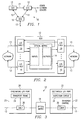
- Figure 1 illustrates a very simplified block diagram of a portion of a communication network 10.
- cross-connect switches shown in Figure 1 as optical cross-connects or "OCXs" 12
- communication lines 13 optical fibers, in this case.
- the cross-connect switches 12 provide flexibility in routing lines. As lines 13 are added or removed, connections between lines 13 can be re-provisioned. Also, the cross-connects switches 12 provide the ability to select between two or more redundant channels, in the event that communications over one of the lines is interrupted or degraded.
- Figure 2 illustrates a cross-connect switch architecture using an optical matrix 14.
- Optical matrix 14 has multiple inputs and multiple outputs.
- the optical matrix 14 is non-blocking, i.e., optical matrix 14 has the ability to switch any of the matrix inputs to any of the matrix outputs regardless of the current cross-connection configuration.
- the inputs and outputs of the matrix are coupled to a plurality of I/O shelves 16, each shelf providing multiple input/output ports for interfacing with lines 13 from the network 10.
- control information including port identification information as well as other information, is modulated on a wavelength different than the wavelength(s) used by the optical data stream from the network and optically multiplexed with the optical data stream from the network in each originating I/O port in shelves 16.
- the control information is formatted in "transport frames" described in greater detail hereinbelow.
- the transport frame is recovered by the destination I/O port to verify the correctness of the path through optical matrix 14.
- the transport frame can be filtered from the output of the destination I/O port, since they are modulated on different wavelengths.
- Figure 3 illustrates a more detailed view of the optical cross connect 12.
- Originating I/O port 20 receives an optical fiber 13 carrying one or more communication channels.
- Optical matrix 14 passes the communication data from this fiber to a desired destination I/O port 22.
- Control information formatted in a transport frame 24, described in greater detail in connection with Figure 4 is modulated onto a predetermined wavelength and optically multiplexed with the optical data signal at the originating port 20 using an optical multiplexer 26.
- the transport frame is modulated at a different frequency than the communication channel(s).
- the transport frame includes information identifying the originating I/O port 20 as well as any other desirable information.
- the communication data and control information is passed to the destination I/O port 22 via the optical matrix 14.
- the destination I/O port 22 includes inspection circuit 28 and optical demultiplexer 30.
- Optical demultiplexer 30 demodulates the transport frame information and translates it into electrical signals.
- Inspection circuit 28 verifies that the information is coming from the correct originating I/O port, based upon the information in the demodulated transport frame.
- the transport frame 24 includes three different classes of information.
- the first class of information is framing information. This information identifies the start of the frame.
- the second class of information is "stuffing" information. The stuffing information ensures that there are enough bit transitions to prevent clock recovery circuits from losing their lock on the data.
- the third class of information is the payload information, which includes any type of information, such as originating I/O port identification, which is desirable to pass from the originating I/O port to the destination I/O port.
- the framing information and the stuffing information are designed to provide fast and unambiguous framing, with a tolerance for bit errors.
- bit errors in the framing and stuffing information do not cause false framing.
- false framing occurs, it is desirable that accurate framing is achieved as soon as possible.
- bit rate for transport channel modulated on fiber 13 is 2 Mbps (megabits per second).
- bit rate for transport channel modulated on fiber 13 is 2 Mbps (megabits per second).
- This signal can be modulated with a 1310 nm laser, which is relatively inexpensive.
- the transport frame 24 is transmitted without scrambling, which would require additional expensive circuitry.
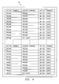
- Figure 4 illustrates a 33-byte transport frame.
- the frame is organized as three framing bytes to start the frame, followed by groups of three bytes (two payload bytes followed by a stuff byte).
- Each of the framing bytes is set to "01010101” and each stuff byte is set to "00110011".
- the last payload byte is a four-bit BIP-4 (or other) error correction byte followed by a predetermined bit pattern (in this case "0101").
- This frame is continually repeated onto a transport channel modulated at a predetermined frequency that will not interfere with the communication channels.
- each frame nineteen bytes of each frame are available for data, such as the originating I/O port identifier.
- a stuff byte ensures data transitions so that clock recovery lock is not lost on the data.
- the stuff bytes also are set to values that make it impossible for payload data to imitate the framing pattern without multiple bit errors.
- the number of framing bytes to indicate the start of the frame could be increased. For example, in a system where five framing bytes are used to indicate the start of the frame, four payload bytes could exist between stuff bits. In general, for a frame using n bytes, n-1 payload bytes can exist prior to a stuff byte. Increasing the number of payload bytes between stuff bytes will not affect false framing (so long as the consecutive framing bytes is similarly increased), however, it could result in a longer time period between bit transitions, which can affect clock recovery.
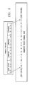
- Figure 5 illustrates detection of the start of the transport packet frame.
- a framing pattern of one stuff byte (the last byte of the previous frame) followed by three framing bytes (for the illustrated embodiment) is detected in the transport channel.
- An important aspect of the embodiment of the transport packet shown in Figure 4 is that it is very difficult for false framing to occur. Assuming that a payload byte could have any value, and thus both payload bytes could have the same value as a framing byte, it would be necessary for the following stuff byte to have, at a minimum, four bit errors in order to mimic the final framing byte necessary for a frame detection.
- the bit pattern after the BIP-4 correction field prevents frames from matching at a half-byte interval.
- a framing pattern will be detected within thirty-six bytes (0.144 milliseconds).
- the inspection circuitry will continue to monitor the framing information at its expected locations (the last stuff byte of the frame and the next consecutive three framing bytes). If two or more consecutive frames are found to have three or more errors in their framing patterns, an "out of frame" condition is declared and the inspection circuit 28 begins looking for a valid frame again. Other criteria may be established based on expected error rates.
- the framing format described above provides a high probability of finding a frame in at least thirty-six bytes, and provides an extremely low probability of false framing. The possibility that false framing occurs for more than one frame is almost non-existent.
- the framing protocol described above provides for a way to transport control information through an optical matrix by modulating a transport channel over the communication channel.
- the transport frame ensures that bit transitions are provided throughout the frame by the inclusion of framing bytes and stuff bytes with known transitions. Thus, other expensive techniques, such as scrambling, can be avoided.
- the framing pattern for detecting the start of a frame is a combination of stuff and pattern bits that require multiple bit errors in order to falsely frame. An in-frame condition is highly likely to occur in less than a millisecond.
- the present invention has also been described in connection with using bytes (eight bits) as the standard unit size.
- the invention could be easily adjusted to accommodate any data unit size.
Landscapes
- Engineering & Computer Science (AREA)
- Computer Networks & Wireless Communication (AREA)
- Time-Division Multiplex Systems (AREA)
Applications Claiming Priority (2)
| Application Number | Priority Date | Filing Date | Title |
|---|---|---|---|
| US638941 | 1991-01-09 | ||
| US09/638,941 US6915078B1 (en) | 2000-08-15 | 2000-08-15 | Optical frame format |
Publications (1)
| Publication Number | Publication Date |
|---|---|
| EP1180911A2 true EP1180911A2 (fr) | 2002-02-20 |
Family
ID=24562079
Family Applications (1)
| Application Number | Title | Priority Date | Filing Date |
|---|---|---|---|
| EP01117080A Withdrawn EP1180911A2 (fr) | 2000-08-15 | 2001-07-13 | Format de trame optique |
Country Status (3)
| Country | Link |
|---|---|
| US (1) | US6915078B1 (fr) |
| EP (1) | EP1180911A2 (fr) |
| CN (1) | CN1338833A (fr) |
Families Citing this family (4)
| Publication number | Priority date | Publication date | Assignee | Title |
|---|---|---|---|---|
| ATE464748T1 (de) * | 2002-01-22 | 2010-04-15 | Microsoft Corp | Verfahren und system zur verhinderung von startkode-emulation und stopfdaten |
| US7221685B2 (en) * | 2002-12-13 | 2007-05-22 | Sbc Properties, L.P. | Method and system relating to bandwidth utilization |
| US10271069B2 (en) | 2016-08-31 | 2019-04-23 | Microsoft Technology Licensing, Llc | Selective use of start code emulation prevention |
| US10498523B1 (en) * | 2018-10-25 | 2019-12-03 | Diodes Incorporated | Multipath clock and data recovery |
Family Cites Families (9)
| Publication number | Priority date | Publication date | Assignee | Title |
|---|---|---|---|---|
| JP2595025B2 (ja) * | 1988-03-18 | 1997-03-26 | 株式会社日立製作所 | 空間分割形スイッチを用いた高速パケット交換装置 |
| US5303078A (en) * | 1990-12-18 | 1994-04-12 | Bell Communications Research, Inc. | Apparatus and method for large scale ATM switching |
| US5754320A (en) * | 1995-08-18 | 1998-05-19 | Nippon Telegraph And Telephone Corporation | Optical cross-connect system |
| US6362905B1 (en) * | 1997-02-24 | 2002-03-26 | Hitachi, Ltd. | Optical crossconnect apparatus and optical transmission system |
| US6631018B1 (en) * | 1997-08-27 | 2003-10-07 | Nortel Networks Limited | WDM optical network with passive pass-through at each node |
| EP1017242B1 (fr) * | 1998-12-28 | 2007-01-31 | STMicroelectronics S.r.l. | Architecture d' interconnexion optique pour des systèmes de télécommunication MRL (WDM) |
| JP2000341728A (ja) * | 1999-05-31 | 2000-12-08 | Fujitsu Ltd | 光クロスコネクト装置 |
| US6477291B1 (en) * | 2001-09-13 | 2002-11-05 | Nayna Networks, Inc. | Method and system for in-band connectivity for optical switching applications |
| JP4030441B2 (ja) * | 2003-02-26 | 2008-01-09 | 富士通株式会社 | 光クロスコネクト装置 |
-
2000
- 2000-08-15 US US09/638,941 patent/US6915078B1/en not_active Expired - Fee Related
-
2001
- 2001-07-13 EP EP01117080A patent/EP1180911A2/fr not_active Withdrawn
- 2001-08-13 CN CN01124793.2A patent/CN1338833A/zh active Pending
Also Published As
| Publication number | Publication date |
|---|---|
| US6915078B1 (en) | 2005-07-05 |
| CN1338833A (zh) | 2002-03-06 |
Similar Documents
| Publication | Publication Date | Title |
|---|---|---|
| US5926303A (en) | System and apparatus for optical fiber interface | |
| RU2176434C2 (ru) | Синхронная цифровая иерархическая сеть | |
| US6525852B1 (en) | Add and drop node for an optical WDM network having traffic only between adjacent nodes | |
| US6832052B1 (en) | Optical transponder | |
| US6570685B1 (en) | Node for optical communication and wavelength-division multiplexing transmission apparatus having a ring structure composed of the same nodes | |
| CN1190026C (zh) | 光交换机和交换光通信信号的方法 | |
| EP1117202A2 (fr) | Procédé de communication de données dans des systèmes de communication | |
| US7839772B2 (en) | Line redundant device and method | |
| US6718141B1 (en) | Network autodiscovery in an all-optical network | |
| US6697546B2 (en) | Optical node system and switched connection method | |
| US20020176130A1 (en) | Optical network with fault/normal pattern tables for identifying location of path failure | |
| US20080253770A1 (en) | Optical transmission device and optical transmission method | |
| EP0827357A2 (fr) | Noeud d'interconnexion de réseau | |
| US6256326B1 (en) | Pseudo-synchronization prevention method in SDH transmission mode, pseudo-synchronization preventing SDH transmission system, and transmitter-receiver in pseudo-synchronization preventing SDH transmission system | |
| US6331989B1 (en) | Multiplex transmission method and system | |
| US6915078B1 (en) | Optical frame format | |
| US7386236B1 (en) | Multiple wavelength TDMA optical network | |
| US7292608B1 (en) | Method and apparatus for transferring synchronous optical network/synchronous digital hierarchy(SONET/SDH) frames on parallel transmission links | |
| FI107672B (fi) | Menetelmä ja järjestely TTI-tunnisteen käsittelyn parantamiseksi | |
| US4365330A (en) | Channel zero switching arrangements for digital telecommunication exchanges | |
| US6870859B1 (en) | Multiplexing system and multiplexing method of tributary signals | |
| US8149687B2 (en) | Intra-node fault recovery within a multi-stage switching architecture | |
| US6262975B1 (en) | Method of auditing cross-connections related to concatenated signals in a synchronous optical network | |
| US7016378B1 (en) | Method and system for automatically provisioning an overhead byte | |
| US7072581B2 (en) | Apparatus and method for signal recognition within WDM optical nodes |
Legal Events
| Date | Code | Title | Description |
|---|---|---|---|
| PUAI | Public reference made under article 153(3) epc to a published international application that has entered the european phase |
Free format text: ORIGINAL CODE: 0009012 |
|
| AK | Designated contracting states |
Kind code of ref document: A2 Designated state(s): AT BE CH CY DE DK ES FI FR GB GR IE IT LI LU MC NL PT SE TR |
|
| AX | Request for extension of the european patent |
Free format text: AL;LT;LV;MK;RO;SI |
|
| STAA | Information on the status of an ep patent application or granted ep patent |
Free format text: STATUS: THE APPLICATION HAS BEEN WITHDRAWN |
|
| 18W | Application withdrawn |
Effective date: 20030829 |