EP1187209A2 - Dispositif electronique avec de composants empilés et methode de fabrication associé - Google Patents
Dispositif electronique avec de composants empilés et methode de fabrication associé Download PDFInfo
- Publication number
- EP1187209A2 EP1187209A2 EP01119748A EP01119748A EP1187209A2 EP 1187209 A2 EP1187209 A2 EP 1187209A2 EP 01119748 A EP01119748 A EP 01119748A EP 01119748 A EP01119748 A EP 01119748A EP 1187209 A2 EP1187209 A2 EP 1187209A2
- Authority
- EP
- European Patent Office
- Prior art keywords
- input
- chip
- stack
- areas
- electronic component
- Prior art date
- Legal status (The legal status is an assumption and is not a legal conclusion. Google has not performed a legal analysis and makes no representation as to the accuracy of the status listed.)
- Withdrawn
Links
Images

Classifications
-
- H—ELECTRICITY
- H10—SEMICONDUCTOR DEVICES; ELECTRIC SOLID-STATE DEVICES NOT OTHERWISE PROVIDED FOR
- H10W—GENERIC PACKAGES, INTERCONNECTIONS, CONNECTORS OR OTHER CONSTRUCTIONAL DETAILS OF DEVICES COVERED BY CLASS H10
- H10W72/00—Interconnections or connectors in packages
-
- H—ELECTRICITY
- H10—SEMICONDUCTOR DEVICES; ELECTRIC SOLID-STATE DEVICES NOT OTHERWISE PROVIDED FOR
- H10W—GENERIC PACKAGES, INTERCONNECTIONS, CONNECTORS OR OTHER CONSTRUCTIONAL DETAILS OF DEVICES COVERED BY CLASS H10
- H10W90/00—Package configurations
-
- H—ELECTRICITY
- H10—SEMICONDUCTOR DEVICES; ELECTRIC SOLID-STATE DEVICES NOT OTHERWISE PROVIDED FOR
- H10W—GENERIC PACKAGES, INTERCONNECTIONS, CONNECTORS OR OTHER CONSTRUCTIONAL DETAILS OF DEVICES COVERED BY CLASS H10
- H10W72/00—Interconnections or connectors in packages
- H10W72/01—Manufacture or treatment
-
- H—ELECTRICITY
- H10—SEMICONDUCTOR DEVICES; ELECTRIC SOLID-STATE DEVICES NOT OTHERWISE PROVIDED FOR
- H10W—GENERIC PACKAGES, INTERCONNECTIONS, CONNECTORS OR OTHER CONSTRUCTIONAL DETAILS OF DEVICES COVERED BY CLASS H10
- H10W72/00—Interconnections or connectors in packages
- H10W72/834—Interconnections on sidewalls of chips
-
- H—ELECTRICITY
- H10—SEMICONDUCTOR DEVICES; ELECTRIC SOLID-STATE DEVICES NOT OTHERWISE PROVIDED FOR
- H10W—GENERIC PACKAGES, INTERCONNECTIONS, CONNECTORS OR OTHER CONSTRUCTIONAL DETAILS OF DEVICES COVERED BY CLASS H10
- H10W90/00—Package configurations
- H10W90/701—Package configurations characterised by the relative positions of pads or connectors relative to package parts
- H10W90/751—Package configurations characterised by the relative positions of pads or connectors relative to package parts of bond wires
- H10W90/754—Package configurations characterised by the relative positions of pads or connectors relative to package parts of bond wires between a chip and a stacked insulating package substrate, interposer or RDL
Definitions
- the invention relates to an electronic component with stacked Building blocks and a method for its production, each module has a chip that is on an intermediate stack level, which is formed by a system carrier, is mounted.
- each stack intermediate level has an adjustable chip selection circuit on.
- this chip selection circuit which for each Intermediate stack level requires a different layout can be stacked by addressing each individual chip Components of the electronic component can be accessed.
- Components stacked in this way have the disadvantage that to design a separate layout for each intermediate level and is to be manufactured. This is not just the risk of confusion the intermediate stack levels when assembling or stacking the building blocks to an electronic component accordingly increased, but the considerable effort for different Constructions of the different management structures on the intermediate stack levels also requires an elevated one Cost of producing an electronic Component with stacked blocks.
- the object of the invention is to have an electronic component specify stacked blocks, in which the effort of Intermediate stack design is significantly reduced and the addressing of the individual blocks on simple Way can be guaranteed. This task is solved with the subject of the independent claims. advantageous Further developments of the invention result from the subclaims.
- the task is performed by an electronic Solved component with stacked blocks, each block has a chip on an intermediate stack level is mounted, and the stack intermediate levels of a stack have identical layout while on the chips irreversible Chip selection circuits adjustable via contact areas are arranged, the irreversible assignment of the contact areas to the intermediate stack levels.
- This solution has the advantage that the chip selection circuit can be minimized and a significantly smaller space requirement claimed as a chip selection circuit based on a Intermediate stack is arranged.
- Another advantage is the identical execution of all stack intermediate levels, what mass production on the one hand is beneficial and on the other hand the cost of the stack intermediate levels reduced.
- the on-chip chip select circuit of the present has a number from breaker circuits to.
- the number of interrupt circuits corresponds at least to the number of intermediate levels in the stack. This has the advantage of being at the chip level the chip addressing is already triggered by triggering the interrupter circuits can be made irreversible, so that different Addressing circuits on the intermediate stack levels can be omitted. It also has the chip selection circuit the advantage on the chip that not from the start the addressing has to be done, but at a suitable one Job in the manufacturing process for the electronic component chip addressing or chip selection are carried out can. The appropriate location depends on the circuit breaker technology and the cheapest time for an irreversible addressing or an irreversible one Assignment of the contact areas to the stack intermediate levels the stacked blocks of an electronic component.
- each breaker circuit via an input line connected with is connected to an input contact area and via an output line, which are connected to an output contact pad is. Via this input contact line or the output contact line can each of the breaker circuits individually triggered so that only one, the stack intermediate level determining interrupt circuit on an addressed chip is not triggered in the chip selection circuit.
- the Interrupt circuits a common output contact area and separate input contact areas.
- Another embodiment of the invention provides that the input contact areas of the circuit breakers bonded wires with input pads on the stack intermediate levels are connected. This embodiment has the advantage of triggering the breaker circuits not directly on the chip via the input contact areas must be triggered, but that input connection surfaces used on the identical intermediate stack levels can be accessed by the opposite the input contact areas larger input connection areas is relieved.
- the input contact areas are on the intermediate stack levels with input contact pins connected which are the stacked building blocks connect. These input pins are consequently after stacking the blocks on top of the stacked ones Modules attached and thus reduce the number of Contact areas and contact connection areas to a minimum Number of input contact pins, over which then a fixed one Access to the individual blocks in the stack is possible becomes.
- the input contact pins are also simultaneous the addressing contacts via which access to the different intermediate levels and chips of the stacked Building blocks from an external circuit, for example on a printed circuit board or a flexible supply bus becomes possible.
- the common one Output contact area of the chip selection circuit via each have a bonded wire with a common output pad connected at the intermediate stack level.
- There all breaker circuits in this embodiment of the invention of a chip is just an output contact area is therefore only on each intermediate level to provide an exit pad.
- the effort for the intermediate stack levels is reduced by individually adapted different addressing circuits on each intermediate stack level on now uniform input connection surfaces and a common output pad at every intermediate stack level.
- the input pads are the stack intermediate levels in the edge area arranged in each stack intermediate level and via input contact pins connected on the sides of the electronic component.
- the edge area of a system carrier on which the intermediate level of the stack is located, metallized at the points, which are connected to the input contact pins should.
- This procedure has the advantage of being simple and economical Way an electronic component with stacked Building blocks can be made, the variety of Interrupt circuits and the multitude of different ones Lines concentrated on just a few input pins over which the individual chips in the different stack intermediate levels are addressable.
- the method has the advantage of being simple Triggering the breaker circuits assigning the Chips are carried out to the individual stack intermediate levels can.
- This method has the advantage of separating the breaker elements in the manufacturing process already on the undivided wafer can be made, or after Separation on the individual chips can be made without that the chips are already on system carriers. in the In principle, however, the separation can preferably be performed using laser technology also at a later point in the manufacturing process be carried out, but no longer if the Blocks are already stacked on top of each other, because in that case access to the breaker elements by means of an evaporation jet is no longer practical.
- the input contact pins are stacked on the side edges Blocks arranged.
- Arranging the contact pins on the side edges of the electronic component the technology with bushings the advantage of a higher Economics, but also the disadvantage that the The number of contact pins that can be accommodated is limited.
- example of the method now all stack intermediate levels with an identical layout manufactured. This identical layout only shows the Input pads and the common output pad for accessing the stacked intermediate levels and has no individual addressing circuits or Chip select circuits.
- This procedure has an economic advantage in particular if Chip selection circuit breaker elements are provided which can be severed by subsequent evaporation, so that the chip selection circuits by means of laser scanning or electron scanning are irreversibly adjustable.
- Another implementation example of the method according to the invention provides that the irreversible assignment after a Application of the chips on a system carrier tape for semiconductor chips by applying an interrupter voltage to a predetermined number of interrupt circuits or one Evaporating a predetermined number of breaker elements he follows.
- the irreversible assignment as long as the chips are still fixed on a system carrier tape has the advantage that immediately after bonding the semiconductor chips and their contact surfaces with the contact connection surfaces of the System carrier tape through the assignment without much effort Application of breaker voltages can take place or through Apply the laser beam technique to cut accordingly prepared breaker elements on the chips.
- To becomes the system carrier tape by structuring a metal tape made with flat conductor patterns.
- the system carrier tape can be made of a metal-clad Foil tape by structuring the metal layer Conductor tracks are made.
- the irreversible assignment takes place after the execution of the Connection preferably after bonding between the contact surfaces arranged on n one behind the other on the system carrier belt Chips and pads on the system carrier tape and before stacking the components into an electronic one Component.
- the system carrier belt is used to stack the components separated into individual system carriers with a chip and accordingly The individual system carriers become the assigned system in the order of the assignment of the stack intermediate levels layered on top of each other.
- the chipselect saves layout costs at chip level, because a uniform layout for all stacking intermediate levels possible, all intermediate stacking levels will be on short-circuited in a simple manner and the output connection or PAD connector for the Chipselect can be on the chip level take place because the definition for the chipselect on the Chip level is provided.
- the circuit breakers can be simple line fuses or fuses that by applying a correspondingly high breaker voltage and thus melt a high current density.
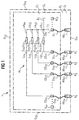
- FIG. 1 shows a schematic diagram in top view of a component 1 comprising a system carrier T 1 and a chip C 1 with a chip selection circuit A 1 on the chip C 1 .
- the dash-dotted line symbolizes the limit G 1 of the chip C 1 .
- the chip C 1 is mounted on a system carrier T 1 , which has the four side edges S 11 , S 12 , S 13 and S 14 .
- a chip select circuit A 1 is arranged, which consists essentially of interrupter circuits U 11 to U 1n or breaker elements E 11 to E 1n, wherein the interrupter circuits U 11 to U 1n and the interrupter elements E 11 to E 1n input lines L 11 to L 1n and output lines LA 11 to LA 1n .
- the output lines LA 11 to LA 1n are connected via a common output line L 1 to an output contact area CS 1 on the chip C 1
- the input lines L 11 to L 1n are routed separately to individual input contact areas CS 11 to CS 1n on the chip C 1
- a further output line B 1 is provided on the chip C 1 , on which, for example, an addressing signal can be forwarded, while the common output line L 1 is used for programming or the irreversible assignment of the chip selection circuit A 1 .
- input terminal areas KA 11 to KA 1n are arranged on the system carrier T 1 in the edge region of the side edge S 11 and are connected to the input contact areas CS 11 to CS 1n on the chip C 1 via bond wires D 11 to D 1n .
- the input contact areas KA 11 to KA 1n contact input contact pins K 1 to K n , which are arranged on the side edge S 11 of the system carrier T 1 .
- An output connection area KA 1 in the edge region of the side edge S 11 of the system carrier T 1 is connected via a bonding wire D 1 to the common output contact area CS 1 of the chip C 1 .
- Further contact areas K11 to K 1m are arranged on the chip C 1 and correspond to the integrated circuit on the chip C 1 .
- one of the interrupter circuits U 11 to U 1n or the interrupter elements E 11 to E 1n is not interrupted in accordance with the number of the intermediate stack level, which are numbered from 1 to n, while the others Interrupt circuits or interrupter elements can be interrupted by impressing an interrupter voltage or by an evaporation treatment and by means of a laser beam or electron beam. This clearly assigns one of the input contact pins K 1 to K n to the address line B 1 .
- FIG. 1 In the embodiment according to FIG.
- the chip selection circuit A 1 is thus arranged on the chip C 1 itself and not on the intermediate stack level Z 1 or on the carrier T 1 , so that all intermediate stack levels Z 1 to Z n of the components 1 - n of the electronic Component can be built completely identical. While the input connection areas KA 11 to KA 1n on the system carrier T 1 are connected to input contact pins K 1 to K n , the common output connection area KA 1 of the modules is not connected to one another by a contact pin, but this output connection area is only used for programming the chip selection circuits A 1 to A n on the chips C 1 to C n .
- FIG. 2 shows a schematic diagram in perspective view of an electronic component composed of n stacked components 1 to n with n chip selection circuits A 1 to A n on the chips C 1 to C n .
- the blocks 1 - n are stacked one above the other.
- the uppermost module 1 in FIG. 2 corresponds to the module in FIG. 1.
- the same reference numerals designate the same construction elements and are therefore not explained again.
- the modules 1 - n each have a system carrier T 1 to T n with an intermediate stack level Z 1 to Z n .
- a chip C 1 to C n is arranged on each system carrier T 1 to T n .
- each chip C 1 to C n has a chip selection circuit A 1 to A n .
- the chip selection circuits A 1 to A n essentially consist of interrupter circuits U 11 to U nn or interrupter elements E 11 to E nn .
- Separate input lines L 11 to L 1n connect the interrupter circuits or the interrupter elements to input contact areas CS 11 to CS nn on the chips C 1 to C n .
- the chips C 1 to C n are semiconductor chips which have at least one integrated circuit. This integrated circuit is addressed via the common output line B 1 to B n of the respective chip selection circuit A 1 to A n .
- the chip selection circuit with a number of interrupter circuits U 11 to U 1n was simultaneously applied, the interrupter circuits having separate input contact areas CS 11 to CS 1n and a common output contact area CS 1 .
- Chips C 1 to C n configured in this way are applied to a system carrier tape with system carriers T 1 to T n arranged one behind the other, wherein the system carrier tape can be a structured metal tape with flat conductor patterns or can consist of a foil tape with metal lamination.
- the metal layer of the metal lamination is structured into conductor tracks and in addition output connection areas and input connection areas are provided on the system carrier tape.
- the chips C 1 to C n are arranged one behind the other on the system carrier tape, they can be provided with bonding wires, the bonding wires for the chip selection circuits A 1 to A n having both the separate input contact areas and the common output contact area of each chip selection circuit A 1 to A n connect to the corresponding input connection areas or output connection areas provided on the system carrier tape.
- this assignment can still be carried out on the system carrier tape by corresponding interruption voltages to the input connection areas KA 11 to KA nn or the output connection areas KA 1 to KA n can be created.
- one of the interrupter circuits U 11 to U nn which is characteristic of the module 1 to n, is not subjected to an interrupter voltage.
- the system carrier tape is separated into individual system carriers and these are stacked with the chips C 1 to C n thereon in the order provided and, as shown in FIG. 2 shows, provided on one of the side edges S 11 to S ln with input contact pins K 1 to K n , which connect the superimposed input connection areas to one another. Due to the irreversible assignment previously carried out with the aid of the chip selection circuits A 1 to A n , the input contact pins K 1 to K n are each clearly connected to one of the address lines B 1 to B n on the chips C 1 to C n .
- the line structure of the system carriers T 1 to T n is identical for all intermediate stack levels Z 1 to Z n , so that a single layout is required for all intermediate stack levels.
Landscapes
- Semiconductor Integrated Circuits (AREA)
- Lead Frames For Integrated Circuits (AREA)
- Fixed Capacitors And Capacitor Manufacturing Machines (AREA)
- Breakers (AREA)
- Design And Manufacture Of Integrated Circuits (AREA)
- Wire Bonding (AREA)
Applications Claiming Priority (2)
| Application Number | Priority Date | Filing Date | Title |
|---|---|---|---|
| DE10044148 | 2000-09-06 | ||
| DE10044148A DE10044148A1 (de) | 2000-09-06 | 2000-09-06 | Elektronisches Bauteil mit gestapelten Bausteinen und Verfahren zu seiner Herstellung |
Publications (2)
| Publication Number | Publication Date |
|---|---|
| EP1187209A2 true EP1187209A2 (fr) | 2002-03-13 |
| EP1187209A3 EP1187209A3 (fr) | 2005-04-13 |
Family
ID=7655338
Family Applications (1)
| Application Number | Title | Priority Date | Filing Date |
|---|---|---|---|
| EP01119748A Withdrawn EP1187209A3 (fr) | 2000-09-06 | 2001-08-27 | Dispositif electronique avec de composants empilés et methode de fabrication associé |
Country Status (7)
| Country | Link |
|---|---|
| US (1) | US6703651B2 (fr) |
| EP (1) | EP1187209A3 (fr) |
| JP (1) | JP3670990B2 (fr) |
| KR (1) | KR100500256B1 (fr) |
| CN (1) | CN1169220C (fr) |
| DE (1) | DE10044148A1 (fr) |
| TW (1) | TW521424B (fr) |
Cited By (1)
| Publication number | Priority date | Publication date | Assignee | Title |
|---|---|---|---|---|
| WO2007078994A3 (fr) * | 2005-12-30 | 2007-08-30 | Micron Technology Inc | Entrees et sorties configurables pour un systeme et un procede d'empilement de mémoire |
Families Citing this family (14)
| Publication number | Priority date | Publication date | Assignee | Title |
|---|---|---|---|---|
| EP1616392A2 (fr) * | 2003-02-28 | 2006-01-18 | Motorola, Inc. | Systeme et procede de transmission de signaux de largeur de bande ultralarge |
| DE10343257B4 (de) * | 2003-09-17 | 2009-06-10 | Qimonda Ag | Verfahren zur Herstellung von Zwischenverbindungen bei Chip-Sandwich-Anordnungen |
| JP4399777B2 (ja) * | 2004-01-21 | 2010-01-20 | セイコーエプソン株式会社 | 半導体記憶装置、半導体装置、及び電子機器 |
| US20060157866A1 (en) * | 2005-01-20 | 2006-07-20 | Le Thoai T | Signal redistribution using bridge layer for multichip module |
| CN101138089B (zh) * | 2005-01-31 | 2011-02-09 | 斯班逊有限公司 | 层叠型半导体装置及层叠型半导体装置的制造方法 |
| US20060202317A1 (en) * | 2005-03-14 | 2006-09-14 | Farid Barakat | Method for MCP packaging for balanced performance |
| DE102005039165B4 (de) * | 2005-08-17 | 2010-12-02 | Infineon Technologies Ag | Draht- und streifengebondetes Halbleiterleistungsbauteil und Verfahren zu dessen Herstellung |
| US7503767B2 (en) * | 2006-08-01 | 2009-03-17 | General Dynamics Advanced Information Systems, Inc. | Method and apparatus for compliantly connecting stack of high-density electronic modules in harsh environments |
| KR20090032845A (ko) * | 2007-09-28 | 2009-04-01 | 삼성전자주식회사 | 반도체 패키지 및 그의 제조방법 |
| US8174841B2 (en) * | 2009-04-27 | 2012-05-08 | International Business Machines Corporation | Adaptive interconnect structure |
| US20110096511A1 (en) * | 2009-10-26 | 2011-04-28 | Christian Krutzik | Ultra-low profile multi-chip module |
| US20110250861A1 (en) * | 2010-04-08 | 2011-10-13 | Viasat, Inc. | Highly integrated, high frequency, high power operation mmic |
| US9472878B2 (en) * | 2015-01-16 | 2016-10-18 | Tyco Electronics Corporation | Electrical cable connector having a two-dimensional array of mating interfaces |
| CN109411453B (zh) * | 2018-09-17 | 2022-03-15 | 珠海欧比特电子有限公司 | 一种三维立体封装的垂直互连方法 |
Family Cites Families (20)
| Publication number | Priority date | Publication date | Assignee | Title |
|---|---|---|---|---|
| KR970003915B1 (ko) * | 1987-06-24 | 1997-03-22 | 미다 가쓰시게 | 반도체 기억장치 및 그것을 사용한 반도체 메모리 모듈 |
| US5198888A (en) * | 1987-12-28 | 1993-03-30 | Hitachi, Ltd. | Semiconductor stacked device |
| US5028986A (en) * | 1987-12-28 | 1991-07-02 | Hitachi, Ltd. | Semiconductor device and semiconductor module with a plurality of stacked semiconductor devices |
| US4996583A (en) * | 1989-02-15 | 1991-02-26 | Matsushita Electric Industrial Co., Ltd. | Stack type semiconductor package |
| US5266834A (en) * | 1989-03-13 | 1993-11-30 | Hitachi Ltd. | Semiconductor device and an electronic device with the semiconductor devices mounted thereon |
| JP2816244B2 (ja) * | 1990-07-11 | 1998-10-27 | 株式会社日立製作所 | 積層型マルチチップ半導体装置およびこれに用いる半導体装置 |
| JPH0513666A (ja) * | 1991-06-29 | 1993-01-22 | Sony Corp | 複合半導体装置 |
| JP2605968B2 (ja) * | 1993-04-06 | 1997-04-30 | 日本電気株式会社 | 半導体集積回路およびその形成方法 |
| JP2526511B2 (ja) * | 1993-11-01 | 1996-08-21 | 日本電気株式会社 | 半導体装置 |
| US5760471A (en) * | 1994-04-20 | 1998-06-02 | Fujitsu Limited | Semiconductor device having an inner lead extending over a central portion of a semiconductor device sealed in a plastic package and an outer lead exposed to the outside of a side face of the plastic package |
| US5698895A (en) * | 1994-06-23 | 1997-12-16 | Cubic Memory, Inc. | Silicon segment programming method and apparatus |
| US5434745A (en) * | 1994-07-26 | 1995-07-18 | White Microelectronics Div. Of Bowmar Instrument Corp. | Stacked silicon die carrier assembly |
| KR0184076B1 (ko) * | 1995-11-28 | 1999-03-20 | 김광호 | 상하 접속 수단이 패키지 내부에 형성되어 있는 3차원 적층형 패키지 |
| US5973396A (en) * | 1996-02-16 | 1999-10-26 | Micron Technology, Inc. | Surface mount IC using silicon vias in an area array format or same size as die array |
| JPH10270634A (ja) * | 1997-03-24 | 1998-10-09 | Mitsubishi Electric Corp | メモリモジュール |
| JP2870530B1 (ja) * | 1997-10-30 | 1999-03-17 | 日本電気株式会社 | スタックモジュール用インターポーザとスタックモジュール |
| JP3563604B2 (ja) * | 1998-07-29 | 2004-09-08 | 株式会社東芝 | マルチチップ半導体装置及びメモリカード |
| US6381141B2 (en) * | 1998-10-15 | 2002-04-30 | Micron Technology, Inc. | Integrated device and method for routing a signal through the device |
| JP3228257B2 (ja) * | 1999-01-22 | 2001-11-12 | 日本電気株式会社 | メモリパッケージ |
| JP3360655B2 (ja) * | 1999-07-08 | 2002-12-24 | 日本電気株式会社 | 半導体装置 |
-
2000
- 2000-09-06 DE DE10044148A patent/DE10044148A1/de not_active Withdrawn
-
2001
- 2001-08-27 EP EP01119748A patent/EP1187209A3/fr not_active Withdrawn
- 2001-08-29 TW TW090121290A patent/TW521424B/zh not_active IP Right Cessation
- 2001-09-06 KR KR10-2001-0054693A patent/KR100500256B1/ko not_active Expired - Fee Related
- 2001-09-06 CN CNB011412518A patent/CN1169220C/zh not_active Expired - Fee Related
- 2001-09-06 US US09/948,261 patent/US6703651B2/en not_active Expired - Lifetime
- 2001-09-06 JP JP2001270931A patent/JP3670990B2/ja not_active Expired - Fee Related
Cited By (5)
| Publication number | Priority date | Publication date | Assignee | Title |
|---|---|---|---|---|
| WO2007078994A3 (fr) * | 2005-12-30 | 2007-08-30 | Micron Technology Inc | Entrees et sorties configurables pour un systeme et un procede d'empilement de mémoire |
| US7352602B2 (en) | 2005-12-30 | 2008-04-01 | Micron Technology, Inc. | Configurable inputs and outputs for memory stacking system and method |
| US7602630B2 (en) | 2005-12-30 | 2009-10-13 | Micron Technology, Inc. | Configurable inputs and outputs for memory stacking system and method |
| US8098508B2 (en) | 2005-12-30 | 2012-01-17 | Round Rock Research, Llc | Configurable inputs and outputs for memory stacking system and method |
| US8559238B2 (en) | 2005-12-30 | 2013-10-15 | Round Rock Research, Llc | Configurable inputs and outputs for memory stacking system and method |
Also Published As
| Publication number | Publication date |
|---|---|
| JP2002164499A (ja) | 2002-06-07 |
| CN1169220C (zh) | 2004-09-29 |
| US20020034069A1 (en) | 2002-03-21 |
| KR20020020225A (ko) | 2002-03-14 |
| DE10044148A1 (de) | 2002-03-21 |
| EP1187209A3 (fr) | 2005-04-13 |
| CN1341965A (zh) | 2002-03-27 |
| JP3670990B2 (ja) | 2005-07-13 |
| US6703651B2 (en) | 2004-03-09 |
| KR100500256B1 (ko) | 2005-07-11 |
| TW521424B (en) | 2003-02-21 |
Similar Documents
| Publication | Publication Date | Title |
|---|---|---|
| DE69800514T2 (de) | Leiterplatte mit primären und sekundären Durchgangslöchern | |
| DE10157280B4 (de) | Verfahren zum Anschließen von Schaltungseinheiten | |
| DE69508835T2 (de) | Dreidimensionale Verbindung von Gehäusen elektronischer Bausteine wobei gedruckte Schaltungen angewendet werden | |
| EP0762496B1 (fr) | Module semi-conducteur de puissance | |
| DE69321864T2 (de) | Verfahren und Vorrichtung zur Verkapselung von dreidimensionalen Halbleiterplättchen | |
| EP1152368B1 (fr) | Carte à puce | |
| EP1187209A2 (fr) | Dispositif electronique avec de composants empilés et methode de fabrication associé | |
| DE68905475T2 (de) | Halbleiter-speichermodul hoeher dichte. | |
| DE102006005645B4 (de) | Stapelbarer Baustein, Bausteinstapel und Verfahren zu deren Herstellung | |
| DE69508379T2 (de) | Zusammenbau einer hochintegrierten schaltung, der leiter eines leiterrahmens mit leitenden bahnen verbindet | |
| DE10138958B4 (de) | Chip-Scale-Packung, gedruckte Leiterplatte, Elektronikmodul und Leiterplatten-Entwurfsverfahren | |
| DE69618872T2 (de) | Integrierte packung mit steckerleitern | |
| DE10142119A1 (de) | Elektronisches Bauteil und Verfahren zu seiner Herstellung | |
| DE68928193T2 (de) | Halbleiterchip und Verfahren zu seiner Herstellung | |
| DE3223619C2 (de) | Halbleiterschaltungsanordnung mit aus polykristallinem Silizium bestehenden Sicherungen | |
| EP0696818B1 (fr) | Dispositif semi-conducteur avec boítier isolant | |
| DE10255289A1 (de) | Elektronisches Bauteil mit gestapelten Halbleiterchips in paralleler Anordnung und Verfahren zu dessen Herstellung | |
| DE3838085A1 (de) | Beschleunigungsfeste verpackung fuer integrierte schaltungen und verfahren zu ihrer herstellung | |
| DE10084657B4 (de) | Modulkarte und Herstellverfahren für diese | |
| DE2753236C2 (de) | Einbaurahmen für eine gehäuselose integrierte Halbleiterschaltungsanordnung | |
| DE69300372T2 (de) | Baugruppe von elektronischen Bauteilen. | |
| EP0964449A2 (fr) | Circuit semiconducteur intégré à structure factice | |
| DE102020116233A1 (de) | Schaltungsträger mit Anschlussflächenfeld und Verfahren zum Herstellen eines Anschlussflächenfelds auf einem Schaltungsträger | |
| DE102004027273A1 (de) | Halbleiterbaustein mit einer ersten und mindestens einer weiteren Halbleiterschaltung und Verfahren | |
| DE10125725B4 (de) | Ball-Grid-Array-Packung |
Legal Events
| Date | Code | Title | Description |
|---|---|---|---|
| PUAI | Public reference made under article 153(3) epc to a published international application that has entered the european phase |
Free format text: ORIGINAL CODE: 0009012 |
|
| AK | Designated contracting states |
Kind code of ref document: A2 Designated state(s): AT BE CH CY DE DK ES FI FR GB GR IE IT LI LU MC NL PT SE TR |
|
| AX | Request for extension of the european patent |
Free format text: AL;LT;LV;MK;RO;SI |
|
| PUAL | Search report despatched |
Free format text: ORIGINAL CODE: 0009013 |
|
| AK | Designated contracting states |
Kind code of ref document: A3 Designated state(s): AT BE CH CY DE DK ES FI FR GB GR IE IT LI LU MC NL PT SE TR |
|
| AX | Request for extension of the european patent |
Extension state: AL LT LV MK RO SI |
|
| 17P | Request for examination filed |
Effective date: 20050714 |
|
| AKX | Designation fees paid |
Designated state(s): DE FR GB IE IT |
|
| 17Q | First examination report despatched |
Effective date: 20050817 |
|
| GRAP | Despatch of communication of intention to grant a patent |
Free format text: ORIGINAL CODE: EPIDOSNIGR1 |
|
| STAA | Information on the status of an ep patent application or granted ep patent |
Free format text: STATUS: THE APPLICATION IS DEEMED TO BE WITHDRAWN |
|
| 18D | Application deemed to be withdrawn |
Effective date: 20090108 |