EP1189112A2 - Appareil d' exposition par projection - Google Patents
Appareil d' exposition par projection Download PDFInfo
- Publication number
- EP1189112A2 EP1189112A2 EP01116994A EP01116994A EP1189112A2 EP 1189112 A2 EP1189112 A2 EP 1189112A2 EP 01116994 A EP01116994 A EP 01116994A EP 01116994 A EP01116994 A EP 01116994A EP 1189112 A2 EP1189112 A2 EP 1189112A2
- Authority
- EP
- European Patent Office
- Prior art keywords
- projection
- exposure system
- projection exposure
- plane
- filter
- Prior art date
- Legal status (The legal status is an assumption and is not a legal conclusion. Google has not performed a legal analysis and makes no representation as to the accuracy of the status listed.)
- Withdrawn
Links
Images
Classifications
-
- G—PHYSICS
- G03—PHOTOGRAPHY; CINEMATOGRAPHY; ANALOGOUS TECHNIQUES USING WAVES OTHER THAN OPTICAL WAVES; ELECTROGRAPHY; HOLOGRAPHY
- G03F—PHOTOMECHANICAL PRODUCTION OF TEXTURED OR PATTERNED SURFACES, e.g. FOR PRINTING, FOR PROCESSING OF SEMICONDUCTOR DEVICES; MATERIALS THEREFOR; ORIGINALS THEREFOR; APPARATUS SPECIALLY ADAPTED THEREFOR
- G03F7/00—Photomechanical, e.g. photolithographic, production of textured or patterned surfaces, e.g. printing surfaces; Materials therefor, e.g. comprising photoresists; Apparatus specially adapted therefor
- G03F7/70—Microphotolithographic exposure; Apparatus therefor
- G03F7/70058—Mask illumination systems
- G03F7/70133—Measurement of illumination distribution, in pupil plane or field plane
-
- G—PHYSICS
- G03—PHOTOGRAPHY; CINEMATOGRAPHY; ANALOGOUS TECHNIQUES USING WAVES OTHER THAN OPTICAL WAVES; ELECTROGRAPHY; HOLOGRAPHY
- G03F—PHOTOMECHANICAL PRODUCTION OF TEXTURED OR PATTERNED SURFACES, e.g. FOR PRINTING, FOR PROCESSING OF SEMICONDUCTOR DEVICES; MATERIALS THEREFOR; ORIGINALS THEREFOR; APPARATUS SPECIALLY ADAPTED THEREFOR
- G03F7/00—Photomechanical, e.g. photolithographic, production of textured or patterned surfaces, e.g. printing surfaces; Materials therefor, e.g. comprising photoresists; Apparatus specially adapted therefor
- G03F7/20—Exposure; Apparatus therefor
-
- G—PHYSICS
- G03—PHOTOGRAPHY; CINEMATOGRAPHY; ANALOGOUS TECHNIQUES USING WAVES OTHER THAN OPTICAL WAVES; ELECTROGRAPHY; HOLOGRAPHY
- G03F—PHOTOMECHANICAL PRODUCTION OF TEXTURED OR PATTERNED SURFACES, e.g. FOR PRINTING, FOR PROCESSING OF SEMICONDUCTOR DEVICES; MATERIALS THEREFOR; ORIGINALS THEREFOR; APPARATUS SPECIALLY ADAPTED THEREFOR
- G03F7/00—Photomechanical, e.g. photolithographic, production of textured or patterned surfaces, e.g. printing surfaces; Materials therefor, e.g. comprising photoresists; Apparatus specially adapted therefor
- G03F7/70—Microphotolithographic exposure; Apparatus therefor
- G03F7/70058—Mask illumination systems
- G03F7/70141—Illumination system adjustment, e.g. adjustments during exposure or alignment during assembly of illumination system
Definitions
- the invention relates to a projection exposure system, especially for microlithography, for production an image one arranged in an object plane Object in an image plane with a projection radiation emitting radiation source, with one in the beam path arranged between the radiation source and the object plane Illumination optics and one in the beam path between of the object plane and the image plane arranged projection optics.
- the lighting intensity is measured by a photosensor, for example the reflection of a optical component of the projection exposure system receives.
- the measurement of an illumination angle distribution is included such a photosensor is not possible.
- the projection radiation can be e.g. projection light optical wavelengths, UV projection light or EUV projection radiation, e.g. Radiation with one wavelength of 13nm.
- An actual state of the is with the detection device Illumination angle distribution measured.
- the measurement of Illumination angle distribution enables at the same time Access to a range of other information at the projection are of interest. For example, allowed they easily determine the telecentricity angle distribution in the measured field level. Further are with the measured illumination angle distribution too the distribution of the numerical aperture of the illuminating light as well as the lighting intensity distribution over the measured field level is known.
- the field level whose illumination angle distribution is measured the object level itself or one of these be conjugate level.
- control device and the at least one assigned manipulator is about the movement of at least an optical component an adaptation of the measured Illumination angle distribution to a default value possible.
- a manipulator can be used for a component or several manipulators can be provided. With With the help of this adjustment is e.g. depending on the too projecting structure optimized lighting of the Possible.
- the detection device can have: a pinhole, which can be arranged in a field level, a position-resolving one Sensor to detect through the pinhole radiation and a drive device Movement of the pinhole together with the sensor in the Field level.
- a pinhole which can be arranged in a field level
- a position-resolving one Sensor to detect through the pinhole radiation
- a drive device Movement of the pinhole together with the sensor in the Field level With this relatively simple design a precise measurement of the illumination angle distribution possible at the field level.
- the diameter of the pinhole specifies the spatial resolution at the field level. through the detection device becomes the drive device traverse the entire field level to be measured.
- Such a detection device can additionally the lighting intensity distribution at the field level measure up.
- the position-resolving sensor can be a CCD array.
- a CCD array is light sensitive and has a high Position resolution on. With the help of known coatings can the sensitivity of the CCD array up to the the micro-lithography interesting illumination wavelength range of the UV wavelengths are expanded. If only a low position resolution for the position resolver Sensor is required, this can also e.g. be designed as a simple quadrant detector.
- the position-resolving Sensor can have at least one optical deflection element be arranged. This reduces the overall depth the detection device in the direction of the optical axis. Especially with projection exposure systems with high structural Integration is the space in which the detection device can be arranged, very limited.
- the filter can comprise a spectral filter, so that e.g. only the lighting wavelength of interest is let through.
- An example of such a filter is a notch filter.
- Other wavelengths that the measurement under certain circumstances, are suppressed.
- the filter can be a gray filter or a reflection filter for neutral attenuation of a have a larger wavelength range.
- Such a lens can e.g. the dissolution of the Increase detection device.
- An optical that works with the manipulator Component can be a filter. With a filter targeted weakening of the projection light beam in certain areas possible.
- the filter can be used as an absorption or be constructed as a reflection filter.
- Filters instead of one Filters with a movable filter component, in which by moving the movable filter component Transmission in the filter plane can be changed also an interchangeable holder for a plurality of interchangeable ones Filters can be provided.
- the filter can be in the area of a field level of the projection optics be arranged. Is the filter in or near arranged at a field level, it affects practically only the lighting intensity distribution in the object plane, but not the illumination angle distribution there.
- the filter can be in the area of a pupil plane the projection optics.
- a thing in or near a pupil plane of the projection optics Arranged filter influences the lighting intensity in this plane and thus serves to specify the illumination angle distribution in the object plane while the Illumination intensity distribution in the object plane is not or is hardly influenced.
- About moving the filter or the movable filter component using the Manipulator is the lighting angle distribution accordingly changed.
- At least one Z manipulator can be used as a manipulator an optical component of the projection optics is provided his.
- the Z direction is the direction in which the optical The axis of the projection optics runs. Also by means of the Z manipulation of optical components is a change the illumination angle distribution possible.
- Such an optical component can be a lens.
- a Z-manipulable lens in addition to the Illumination angle distribution is also an aberration the projection exposure system corrected become.
- Another such Z-manipulated optical component can be an axicon. With the help of an axicon you can simple way a controlled changeable rotationally symmetrical Illumination angle distribution can be set.
- a manipulable optical component can be an adjustment device the radiation source.
- Adjustment device for example, the divergence of the projection radiation beam emitted by the radiation source can be set. This is an additional one Influence parameters for the illumination angle distribution.
- the manipulator can have a piezo element.
- Piezo elements can be reproducible and precise Achieve relocation. Become multiple piezo elements used to manipulate an optical component, In addition to the Z position, the inclination of the adjust the optical component against the optical axis.
- optical components are used to influence the illumination angle distribution other conceivable.
- examples for these are wedge plates that can be shifted against each other, tiltable or Z-manipulable plane-parallel optical plates, Aperture diaphragms with variable opening or, in the case of catadioptric ones Projection lenses, active mirrors.
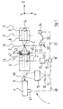
- Figure 1 is schematically one overall with the reference symbol 1 provided projection exposure system for the Microlithography presented. With this one Structure on a reticle 2 on the surface of a Transfer Wafers 3.
- a radiation source for the projection exposure system 1 is a UV laser 4, e.g. an ArF excimer laser with a wavelength of 193.3 nm.
- a controlled adjustment device is coupled to the UV laser 4 47. This is e.g. for one or several micrometer screws coupled with one actuator.
- the adjustment device 47 is on an optical component of the UV laser 4 and arranged via a control line 48 connected to a control device 18.
- a projection light beam emitted by the UV laser 4 5 first enters an illumination optics 6.
- the beam path of the projection light beam 5 is for clarity because only between the UV laser 4 and the Illumination optics 6 indicated.
- the lighting optics 6 is shown schematically for the most part as a block in FIG and in addition to lenses and possibly also mirrors
- a number of other optical elements or assemblies, e.g. B. a zoom lens, an axicon, a sliding wedge plate, diffractive optical elements, a filter and one Glass rod for specifying a lighting intensity distribution and an illumination angle distribution of the projection light beam 5 have. All of these optical Components can be relocated in a controlled manner.
- Representing an optical element within a lens 41 is shown for the illumination optics 6, which are arranged in a lens frame 42 comprising them is.
- the lens frame is not shown 42 biased against a retaining ring 43.
- the latter is on its outer peripheral surface firmly with a housing the lighting optics 6 connected.
- Piezo actuators 44 In the axial direction to the illumination optics 6 is between the lens frame 42 and the retaining ring 43 a group of Piezo actuators 44 arranged. This includes several individual piezo actuators 45, two of which are shown in FIG. 1 are shown. Over a multi-pole, dash-dotted shown control line 46 are the piezo actuators 45 with the control device 18 in connection.
- the pupil plane 13 is also referred to below as the filter level.
- the projection light bundle leaving the illumination optics 6 5 illuminates the reticle 2.
- the structures of the Reticles 2 are opened with the aid of projection optics 8 projected the surface of the wafer 3.
- the projection optics 8 can consist of a plurality of lenses and / or Be built up mirroring.
- a selected, a central object point on the Reticle 2 passing through and with the projection optics 8 guided imaging light beam is in Figure 1 with the Provided reference numeral 9 and to illustrate the Imaging beam path a bit in the opposite direction, that is, in the direction of and into the illumination optics 6 extended.
- the reticle 2 lies in the object plane 10 of FIG Projection optics 8, shown in Figure 1 by a dashed line Line is indicated.
- the object plane 10 coincides with a Collimation plane of the projection light beam 5 together.
- the wafer 3 is also in a dashed line Line indicated image plane 11 of the projection optics 8.
- a pupil plane 12 of the projection optics 8 is in Figure 1 also indicated schematically. It is for Filter plane 13 conjugated in the illumination optics 6.
- the optical axis of the projection exposure system is also indicated by dashed lines in FIG. 1 and provided with the reference number 14. It runs in the Z direction of the Cartesian shown on the right in Fig. 1 Coordinate system X, Y and Z.
- a partially transmissive optical disk 49 arranged a small proportion of the projection light beam 5 reflected and the vast majority, in in practice more than 99% of the projection light beam 5 transmitted.
- the beam path of the optical disc 49 passing through projection light beam 5 is because it not interested here, just a little bit further continued with dashed lines.
- Proportion of the projection light bundle 5 according to the optical one Plate 49 is placed on an imaging optics 15 two-dimensional CCD array 16 shown. With this can thus the intensity distribution of the projection light beam 5 can be included.
- the CCD array 16 stands over a dash-dotted line Signal line 17 with the control device 18 in Connection.
- Detection device 30 for measuring the illumination intensity and the illumination angle distribution of the imaging bundle 9 in the object plane 10 is in Figure 1 in an inactive position outside the projection beam path shown.
- the detection device 30 in the X, Y plane perpendicular to the optical axis 14, as shown by the double arrow 31, after removal of the reticle 2 is inserted into the beam path in this way be that an inlet opening designed as a pinhole 32 lies in the object plane 10.
- imaging bundle illuminating the reticle 9 enter the inside of the detection device 30.
- the detection device 30 is flexible Signal line 33 with a detection control device 34 connected, which in turn is shown by a dash-dotted line Signal line 35 with the control device 18 communicates.
- the control device 18 controls via a signal line 19, which is also shown in broken lines, one Drive device 20, which is also dash-dotted shown drive connection 21 a twist an element of the pupil filter 7 around the optical axis 14 accomplished.
- the rotatable element of the pupil filter does not have one about the axis of rotation rotationally symmetrical transmission distribution.
- control device 18 controls via a control line 48 the adjustment device 47 for shifting the associated optical component of the UV laser 4.
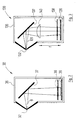
- the image bundle 9 is 90 ° from a mirror 37 diverted. This is done due to space constraints to the overall length the detection device 30 in the direction of the optical Reduce axis 14. After reflection on mirror 37 the imaging bundle 9 passes through a spectral filter 38, that transmits the wavelength of the imaging beam 9, blocks other wavelengths, however.
- An example for the spectral filter 38 is a notch filter. After stepping through of the spectral filter 38 and possibly another one, not filter shown for non-color selective attenuation of the imaging bundle 9 meets a two-dimensional one CCD array 39.
- the z. B. of the type can be "front illuminated" for the spectral range increase for illumination wavelengths less than 350 nm, is a phosphor layer on the CCD chip surface aufsedimentiert.
- the detection device 30 works as follows:
- the detection device 30 After removing the reticle 2, the detection device 30 in the exposed area of the object plane 10 retracted. Then with homogeneous lighting a fine adjustment by the projection light beam 5 in the direction of the optical axis 14 (Z direction) performed until the level of the inlet opening 32 with the Object level 10 matches.
- the detector control device 34 controlled fine adjustment the entry opening 32 with a fixed X and Y position Move step by step in the Z direction.
- the travel range in the Z direction is specified so that the object plane 10 and thus also the collimation plane of the projection light beam 5 lies safely in the travel range. With every step the amount of illumination light incident on the CCD array 39, that is, the one coming through the inlet opening 32 Share of the image bundle 9, integrated and read out.
- the Z position of the entry opening 32 at which the maximum amount of illumination light read is controlled by the detector controller 34 with which Entry opening 32 approached.
- This fine adjustment process can be done at different X, Y positions be repeated.
- the detection device 30 is in the this Z position belonging X, Y plane in a grid pattern over the entire illuminated area of the object plane in the X and Y directions scanned. This is also controlled by the detector control device 34, which is also the grid step size pretends. At each grid point, the from the two pixels of the individual pixels of the CCD array 39 Intensity distribution of each Image bundle 9 belonging to the raster point is read out.
- the intensity distribution recorded at the grid point corresponds to the imaging light distribution of an object point on the reticle 2, which with reticle 2 inserted assumes the position of the grid point, is exposed. It can be evaluated as follows:
- the size of the exposed area on the CCD array 39 is a direct measure of the numerical aperture of the imaging bundle 9 at the respective grid point.
- the intensity distribution the illuminated area on the CCD array 39 finally provides direct information about the Illumination angle distribution for the imaging bundle 9 at the respective grid point.
- This data is sent via the signal line 33 of the detector control device 34 supplied in which the actual values the intensity distribution, the numerical aperture, the Telecentricity angle distribution and the illumination angle distribution compared with predetermined target values become.
- the drive device 20 for the pupil filter 7 and the Actuator group 44 for the lens 41 via the signal lines 48, 19 and 46 and the control device 18 driven.
- the projection exposure system 1 works as follows:
- the lighting intensity distribution and the lighting angle distribution of the projection light beam 5 in the Object plane 10 containing reticle 2 should look like.
- the illumination angle distribution in the object plane 10 is an intensity distribution of the projection light beam 5 assigned in the pupil plane 13.
- the one to reach there a desired illumination angle distribution The intensity distribution to be set can e.g. a constant Intensity course over the bundle profile.
- any number can also be used other intensity distributions of the light beam 5 in the Pupil level 13, so-called lighting settings, specified become.
- an annular lighting setting i.e. a type of lighting, where the intensity distribution in the pupil plane 13 in an annular area around the optical axis 14 has the greatest intensity.
- the structure on the reticle 2 are also other lighting settings adjustable for optimal projection, e.g. with multiple symmetry in the circumferential direction.
- An example for the latter type of lighting is quadrupole lighting.
- a desired lighting intensity distribution in the object level is e.g. a homogeneous Intensity distribution of the projection light beam 5.
- a desired telecentricity angle distribution is, for example a heavy beam parallel to the optical axis 14 for all object points, i.e. one on the object side telecentric lighting optics 6.
- a desired numerical aperture of the projection light beam 5 uses e.g. the numerical aperture of the lighting optics completely out. This type of lighting is with a homogeneous distribution of lighting intensity and illumination angle distribution than conventional Lighting setting known. Alternatively, too a numerical aperture of the projection light beam 5 desired, which is significantly smaller than that of Illumination optics 6. In this case one speaks of one coherent lighting setting.
- control devices 18 and 34 are fed automatically.
- Such input variables are e.g. structural information associated with the respective reticle, which, for example, have one on the Reticle 2 attached barcode can be read, or information about environmental parameters such as pressure, Temperature or humidity by appropriate Sensors are provided.
- Results for example, that measured with the CCD array Intensity distribution of the projection light beam 5, that the UV laser must be readjusted corresponding control of the adjustment device 47.
- the effects of the adjustment can be viewed online through the CCD array 39 are tracked.
- the movable ones are available to change the lighting settings Element of the pupil filter 7 and that of the actuator group 44 manipulable lens 41 available.
- the numerical aperture can also be adjusted using the adjustment device 47 can be adjusted.
- the control device 18 is used to change the Lighting settings, for example the drive device 20 controlled so that the rotation of the rotatable filter element of the pupil filter 7 of the desired Transmission course sets.
- the telecentricity angle distribution or the heavy beam course the image bundle can be manipulated by the Actuator group 44 are influenced. It can by simultaneous change in length of the piezo actuators 45 .mu.m the same amount in the Z direction a corresponding Z manipulation the lens 41. However, the Piezo actuators 45 differently via the control line 46 driven, the inclination of the axis of symmetry Lens 41 can be adjusted to the optical axis 14.
- a lighting intensity curve in the object plane 10 can alternatively or additionally another filter with a movable filter element near a field level, e.g. B. near the object plane 10, be used.
- a filter is for homogenization the lighting intensity in the object plane 10 known.
- the detection device the illumination angle distribution and the Illumination intensity distribution in the object plane 10 can be measured.
- the CCD array 39 the intensity distribution in any other lighting level the projection exposure system 1 are recorded. Examples of such levels are the image level 3 or the pupil planes 12, 13.
- FIG. 3 An alternative detection device for measuring the Illumination distribution of the projection exposure system 1 in the object plane 10 is subsequently described with reference to FIG. 3 described.
- a detection device 130 is between the Deflecting mirror 137 and the spectral filter 138 a lens 140 arranged with positive refractive power.
- the lens increases given the size of the housing 136, the maximum measurable Telecentric angle and increases the angular resolution as well Imaging bundle 109, due to a larger telecentricity angle inclined relatively strongly to the optical axis are still directed towards the CCD array 139.
Landscapes
- Physics & Mathematics (AREA)
- General Physics & Mathematics (AREA)
- Exposure And Positioning Against Photoresist Photosensitive Materials (AREA)
- Exposure Of Semiconductors, Excluding Electron Or Ion Beam Exposure (AREA)
- Length Measuring Devices By Optical Means (AREA)
- Testing Of Optical Devices Or Fibers (AREA)
- Microscoopes, Condenser (AREA)
Applications Claiming Priority (2)
| Application Number | Priority Date | Filing Date | Title |
|---|---|---|---|
| DE10046218A DE10046218B4 (de) | 2000-09-19 | 2000-09-19 | Projektionsbelichtungsanlage |
| DE10046218 | 2000-09-19 |
Publications (2)
| Publication Number | Publication Date |
|---|---|
| EP1189112A2 true EP1189112A2 (fr) | 2002-03-20 |
| EP1189112A3 EP1189112A3 (fr) | 2005-04-06 |
Family
ID=7656706
Family Applications (1)
| Application Number | Title | Priority Date | Filing Date |
|---|---|---|---|
| EP01116994A Withdrawn EP1189112A3 (fr) | 2000-09-19 | 2001-07-12 | Appareil d' exposition par projection |
Country Status (5)
| Country | Link |
|---|---|
| US (1) | US6636367B2 (fr) |
| EP (1) | EP1189112A3 (fr) |
| JP (1) | JP2002175980A (fr) |
| KR (1) | KR20020022559A (fr) |
| DE (1) | DE10046218B4 (fr) |
Cited By (4)
| Publication number | Priority date | Publication date | Assignee | Title |
|---|---|---|---|---|
| EP1462780A1 (fr) * | 2003-03-28 | 2004-09-29 | Canon Kabushiki Kaisha | Dispositif et procédé pour mesurer la distribution d'intensité lumineuse dans l'UV extrème |
| EP1584983A3 (fr) * | 2004-04-07 | 2007-02-28 | Canon Kabushiki Kaisha | Appareil d'exposition et méthode de fabrication d'un dispositif |
| WO2008089898A1 (fr) * | 2007-01-23 | 2008-07-31 | Carl Zeiss Smt Ag | Appareil de mesure de distribution de puissance de rayonnement et procédé de mesure |
| WO2009000241A3 (fr) * | 2007-06-22 | 2009-02-19 | Josef Lindthaler | Dispositif d'exposition par contact d'un pochoir |
Families Citing this family (20)
| Publication number | Priority date | Publication date | Assignee | Title |
|---|---|---|---|---|
| US6930274B2 (en) * | 2003-03-26 | 2005-08-16 | Siemens Vdo Automotive Corporation | Apparatus and method of maintaining a generally constant focusing spot size at different average laser power densities |
| DE10329793A1 (de) * | 2003-07-01 | 2005-01-27 | Carl Zeiss Smt Ag | Projektionsobjektiv für eine mikrolithographische Projektionsbelichtungsanlage |
| JP4262032B2 (ja) | 2003-08-25 | 2009-05-13 | キヤノン株式会社 | Euv光源スペクトル計測装置 |
| US7023524B2 (en) * | 2003-12-18 | 2006-04-04 | Asml Netherlands B.V. | Lithographic apparatus and device manufacturing method |
| JP4497949B2 (ja) * | 2004-02-12 | 2010-07-07 | キヤノン株式会社 | 露光装置 |
| JP2005233827A (ja) * | 2004-02-20 | 2005-09-02 | Canon Inc | Euv光強度分布測定装置およびeuv光強度分布測定方法 |
| JP4684563B2 (ja) | 2004-02-26 | 2011-05-18 | キヤノン株式会社 | 露光装置及び方法 |
| DE102004063314A1 (de) * | 2004-12-23 | 2006-07-13 | Carl Zeiss Smt Ag | Filtereinrichtung für die Kompensation einer asymmetrischen Pupillenausleuchtung |
| US7505152B2 (en) * | 2005-02-24 | 2009-03-17 | The Boeing Company | Optical metrology system |
| US20060209410A1 (en) * | 2005-03-18 | 2006-09-21 | Smith Adlai H | Method and apparatus for compensation or amelioration of lens field curvature and other imaging defects by utilizing a multi-wavelength setting illumination source |
| US7967452B2 (en) * | 2005-08-26 | 2011-06-28 | Panasonic Corporation | Projection type display apparatus |
| US7329876B2 (en) * | 2006-01-26 | 2008-02-12 | Xtreme Technologies Gmbh | Narrow-band transmission filter for EUV radiation |
| US20070229944A1 (en) * | 2006-03-31 | 2007-10-04 | Lee Sang H | Reducing extreme ultraviolet flare in lithographic projection optics |
| EP1906252A1 (fr) * | 2006-09-28 | 2008-04-02 | Carl Zeiss SMT AG | Instrument de mesure de la répartition angulaire de la lumière produite par un système d'illumination d'un appareil d'exposition par projection microlithographique |
| US7990520B2 (en) * | 2006-12-18 | 2011-08-02 | Carl Zeiss Smt Gmbh | Microlithography illumination systems, components and methods |
| WO2008092653A2 (fr) * | 2007-01-30 | 2008-08-07 | Carl Zeiss Smt Ag | Système d'éclairage d'un appareil d'exposition par projection pour microlithographie |
| US7960701B2 (en) * | 2007-12-20 | 2011-06-14 | Cymer, Inc. | EUV light source components and methods for producing, using and refurbishing same |
| DE102008011501A1 (de) | 2008-02-25 | 2009-08-27 | Carl Zeiss Smt Ag | Verfahren zum Betreiben eines Beleuchtungssystems einer mikrolithographischen Projektionsbelichtungsanlage |
| WO2012097833A1 (fr) | 2011-01-20 | 2012-07-26 | Carl Zeiss Smt Gmbh | Procédé d'actionnement d'un outil d'exposition par projection |
| JP6952136B2 (ja) | 2017-07-10 | 2021-10-20 | エーエスエムエル ネザーランズ ビー.ブイ. | リソグラフィの方法及び装置 |
Family Cites Families (6)
| Publication number | Priority date | Publication date | Assignee | Title |
|---|---|---|---|---|
| US5420417A (en) * | 1991-10-08 | 1995-05-30 | Nikon Corporation | Projection exposure apparatus with light distribution adjustment |
| JPH0729816A (ja) * | 1993-07-14 | 1995-01-31 | Canon Inc | 投影露光装置及びそれを用いた半導体素子の製造方法 |
| JP2809081B2 (ja) * | 1993-12-27 | 1998-10-08 | 日本電気株式会社 | 露光装置 |
| KR980005334A (ko) * | 1996-06-04 | 1998-03-30 | 고노 시게오 | 노광 방법 및 노광 장치 |
| JP3262039B2 (ja) * | 1997-07-18 | 2002-03-04 | キヤノン株式会社 | 露光装置及びそれを用いたデバイスの製造方法 |
| US6281967B1 (en) | 2000-03-15 | 2001-08-28 | Nikon Corporation | Illumination apparatus, exposure apparatus and exposure method |
-
2000
- 2000-09-19 DE DE10046218A patent/DE10046218B4/de not_active Expired - Fee Related
-
2001
- 2001-07-12 EP EP01116994A patent/EP1189112A3/fr not_active Withdrawn
- 2001-08-23 KR KR1020010050834A patent/KR20020022559A/ko not_active Ceased
- 2001-09-19 US US09/955,921 patent/US6636367B2/en not_active Expired - Fee Related
- 2001-09-19 JP JP2001284478A patent/JP2002175980A/ja active Pending
Cited By (5)
| Publication number | Priority date | Publication date | Assignee | Title |
|---|---|---|---|---|
| EP1462780A1 (fr) * | 2003-03-28 | 2004-09-29 | Canon Kabushiki Kaisha | Dispositif et procédé pour mesurer la distribution d'intensité lumineuse dans l'UV extrème |
| EP1584983A3 (fr) * | 2004-04-07 | 2007-02-28 | Canon Kabushiki Kaisha | Appareil d'exposition et méthode de fabrication d'un dispositif |
| WO2008089898A1 (fr) * | 2007-01-23 | 2008-07-31 | Carl Zeiss Smt Ag | Appareil de mesure de distribution de puissance de rayonnement et procédé de mesure |
| US8537332B2 (en) | 2007-01-23 | 2013-09-17 | Carl Zeiss Smt Gmbh | Projection exposure tool for microlithography with a measuring apparatus and method for measuring an irradiation strength distribution |
| WO2009000241A3 (fr) * | 2007-06-22 | 2009-02-19 | Josef Lindthaler | Dispositif d'exposition par contact d'un pochoir |
Also Published As
| Publication number | Publication date |
|---|---|
| KR20020022559A (ko) | 2002-03-27 |
| US20020085286A1 (en) | 2002-07-04 |
| EP1189112A3 (fr) | 2005-04-06 |
| US6636367B2 (en) | 2003-10-21 |
| DE10046218A1 (de) | 2002-04-25 |
| JP2002175980A (ja) | 2002-06-21 |
| DE10046218B4 (de) | 2007-02-22 |
Similar Documents
| Publication | Publication Date | Title |
|---|---|---|
| DE10046218B4 (de) | Projektionsbelichtungsanlage | |
| DE10120446C2 (de) | Projektionsbelichtungsanlage sowie Verfahren zur Kompensation von Abbildungsfehlern in einer Projektionsbelichtungsanlage, insbesondere für die Mikro-Lithographie | |
| EP2064597B1 (fr) | Systeme d'eclairage avec un detecteur pour capter une intensite de lumiere | |
| EP1186956A2 (fr) | Appareil d' exposition par projection | |
| EP1130470A2 (fr) | Illumination de projection microlithographique avec polarisation tangentielle | |
| WO2008061681A2 (fr) | Optique d'éclairage pour la microlithographie par projection et procédé de mesure et de contrôle pour une telle optique d'éclairage | |
| DE10109929A1 (de) | Vorrichtung zur Wellenfronterfassung | |
| DE102004063314A1 (de) | Filtereinrichtung für die Kompensation einer asymmetrischen Pupillenausleuchtung | |
| DE102010047050A1 (de) | Verfahren zur Charakterisierung einer Struktur auf einer Maske und Vorrichtung zur Durchführung des Verfahrens | |
| DE102008040742A1 (de) | Verfahren und Vorrichtung zur Überwachung von Mehrfachspiegelanordnungen, optische Anordnung mit einer derartigen Vorrichtung sowie mit einer zweiten Mehrfachspiegelanordnung zum Ein- und Ausschalten einer ersten Mehrfachspiegelanordnung sowie Beleuchtungsoptik für eine Projektionsbelichtungsanlage mit einer derartigen Vorrichtung | |
| WO2009121541A1 (fr) | Dispositif d'éclairage microlithographique par projection, et dispositif d'inspection d'une surface d'un substrat | |
| DE10140208A1 (de) | Optische Anordnung | |
| DE102021206203A1 (de) | Heizanordnung und Verfahren zum Heizen eines optischen Elements | |
| DE102022210158A1 (de) | Anordnung, Verfahren und Computerprogrammprodukt zur Kalibrierung von Facettenspiegeln | |
| EP3827312B1 (fr) | Procédé et dispositif pour la détermination de la condition de chauffage d'un élément optique dans un système optique pour la microlithographie | |
| DE102018124314B4 (de) | Vorrichtung zur Bestimmung der Belichtungsenergie bei der Belichtung eines Elements in einem optischen System, insbesondere für die Mikrolithographie | |
| DE102012212194B4 (de) | Mikrolithographische Projektionsbelichtungsanlage und Verfahren zur Veränderung einer optischen Wellenfront in einem katoptrischen Objektiv einer solchen Anlage | |
| WO2019057708A1 (fr) | Procédé de caractérisation d'au moins un composant optique d'une installation de lithographie par projection | |
| WO2024068293A1 (fr) | Réflectomètre euv et procédé de mesure | |
| DE102022203369A1 (de) | Anordnung, Verfahren und Computerprogrammprodukt zur Kalibrierung von Facettenspiegeln | |
| DE102012213794A1 (de) | Maskeninspektionsverfahren und Maskeninspektionssystem für EUV-Masken | |
| DE102012219169B4 (de) | Strahlregelungsvorrichtung für einen Beleuchtungsstrahl, optisches System mit einer derartigen Strahlregelungsvorrichung sowie Metrologiesystem mit einem eine solche Strahlregelungsvorrichtung enthaltenden optischen System | |
| DE102005025535A1 (de) | Vorrichtung und Verfahren zur Verbesserung der Messgenauigkeit bei der Bestimmung von Strukturdaten | |
| DE102013200394A1 (de) | Polarisationsmessvorrichtung, Lithographieanlage, Messanordnung, und Verfahren zur Polarisationsmessung | |
| DE102011082481A1 (de) | Beleuchtungssystem einer mikrolithographischen projektionsbelichtungsanlage und verfahren zu deren betrieb |
Legal Events
| Date | Code | Title | Description |
|---|---|---|---|
| PUAI | Public reference made under article 153(3) epc to a published international application that has entered the european phase |
Free format text: ORIGINAL CODE: 0009012 |
|
| AK | Designated contracting states |
Kind code of ref document: A2 Designated state(s): AT BE CH CY DE DK ES FI FR GB GR IE IT LI LU MC NL PT SE TR |
|
| AX | Request for extension of the european patent |
Free format text: AL;LT;LV;MK;RO;SI |
|
| RAP1 | Party data changed (applicant data changed or rights of an application transferred) |
Owner name: CARL ZEISS SMT AG |
|
| PUAL | Search report despatched |
Free format text: ORIGINAL CODE: 0009013 |
|
| AK | Designated contracting states |
Kind code of ref document: A3 Designated state(s): AT BE CH CY DE DK ES FI FR GB GR IE IT LI LU MC NL PT SE TR |
|
| AX | Request for extension of the european patent |
Extension state: AL LT LV MK RO SI |
|
| AKX | Designation fees paid | ||
| 17P | Request for examination filed |
Effective date: 20051006 |
|
| RBV | Designated contracting states (corrected) |
Designated state(s): DE FR NL |
|
| REG | Reference to a national code |
Ref country code: DE Ref legal event code: 8566 |
|
| RAP1 | Party data changed (applicant data changed or rights of an application transferred) |
Owner name: CARL ZEISS SMT AG |
|
| STAA | Information on the status of an ep patent application or granted ep patent |
Free format text: STATUS: THE APPLICATION IS DEEMED TO BE WITHDRAWN |
|
| 18D | Application deemed to be withdrawn |
Effective date: 20100202 |