EP1189376A2 - Optischer Wellenlängenmultiplex-Sender, optischer Wellenlängenmultiplex-Empfänger, optische Übertragungsvorrichtung, und optisches Übertragungssystem - Google Patents
Optischer Wellenlängenmultiplex-Sender, optischer Wellenlängenmultiplex-Empfänger, optische Übertragungsvorrichtung, und optisches Übertragungssystem Download PDFInfo
- Publication number
- EP1189376A2 EP1189376A2 EP01122020A EP01122020A EP1189376A2 EP 1189376 A2 EP1189376 A2 EP 1189376A2 EP 01122020 A EP01122020 A EP 01122020A EP 01122020 A EP01122020 A EP 01122020A EP 1189376 A2 EP1189376 A2 EP 1189376A2
- Authority
- EP
- European Patent Office
- Prior art keywords
- optical
- signal
- division multiplex
- wavelength division
- frequency
- Prior art date
- Legal status (The legal status is an assumption and is not a legal conclusion. Google has not performed a legal analysis and makes no representation as to the accuracy of the status listed.)
- Withdrawn
Links
Images


Classifications
-
- H—ELECTRICITY
- H04—ELECTRIC COMMUNICATION TECHNIQUE
- H04J—MULTIPLEX COMMUNICATION
- H04J14/00—Optical multiplex systems
- H04J14/02—Wavelength-division multiplex systems
- H04J14/0298—Wavelength-division multiplex systems with sub-carrier multiplexing [SCM]
Definitions
- the invention relates to a wavelength division multiplex optical transmitter, a wavelength division multiplex optical receiver, an optical transmission device and an optical transmission system, which are used for optical communication, CATV, optical measurement, and mobile communication, for example.
- signals on multiple channels are electrically multiplexed into an AM signal with a plurality of sub-carriers each having a different frequency. Then, the AM signal is converted into an optical signal with direct modulation of a semiconductor laser and the like, and the optical signal is transmitted through an optical fiber.
- the optical transmission of video under an AM signal requires that the receiver receives high optical input power to obtain a C/N value (carrier-to-noise ratio) for ensuring desired video quality, though the modulator and demodulator (MODEM) therefor is simple in the configuration and of low cost.
- C/N value carrier-to-noise ratio
- the intensity level of voice and data signals to be transmitted is largely changed depending on the movement of the terminal, so that a wide dynamic range with respect to signal changes is necessary.
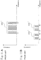
- Figure 10 is a block diagram of a conventional optical-transmission system. Further, Figure 11A shows a frequency arrangement diagram of a conventional transmission signal, and Figure 11B shows a frequency arrangement diagram of nonlinear distortion signals generated therein.
- a multi-channel signal group 3000' is frequency-multiplexed into a plurality of sub-carriers over the range of frequencies from f1' to f4' (see Figure 11A), and then converted into optical signals by an electricity-to-light conversion portion 1001 of an optical transmitter 1000. Then, the optical signals are propagated through an optical fiber 20 and input into a light-to-electricity conversion portion 2001 of an optical receiver 2000, in which the optical signals are converted into electrical signals, and the electrical signals are took out therefrom.
- the frequency band f5' to f6' of the second-order intermodulation distortion 3002' exists on the lower frequency side than the frequency band f1' to f4' of the signal group 3000', and the frequency band f7' to f8' of the third-order intermodulation distortion (IM3) 3003' exists within the frequency band f1' to f4' of the signal group 3000'.
- IM3 third-order intermodulation distortion
- the band of the second-order intermodulation distortion 3002' determined by the components of differential frequencies (i.e. a difference between f4' and fl') between the frequency bands, becomes broader due to he signal band broadened by the increase of the number of channels to overlap with the signal band (that is, f6' shifts to higher frequency side and gets close to f1', overlapping with the frequency band of the signal group 3000').
- the maximum level of the third-order inetrmodulation distortion 3003' existing within the band of the signal group 3003' becomes larger by one number of composites determined by the number of channels to be multiplexed.
- intermodulation distortion (refereed to as distortion components) existing within the signal band also increases.
- distortion components there has been a problem that it becomes difficult to get a desired value of C/N during receiving.
- an object of the present invention is to provide a wavelength division multiplex optical transmitter, a wavelength division multiplex optical receiver, an optical transmission device and an optical transmission system which can ensure a high value of C/N (carrier-to-noise ratio) even in increased number of channels.
- the 1st invention of the present invention is a wavelength division multiplex optical transmitter, comprising:
- the 2nd invention of the present invention is the wavelength division multiplex optical transmitter according to 1st invention, wherein said dividing is performed such that a difference between the highest frequency and the lowest frequency in each frequency band of said plurality of frequency bands may be smaller than the difference between the highest frequency and the lowest frequency of said incoming frequency-multiplexed electrical signal.
- the 3rd invention of the present invention is the wavelength division multiplex optical transmitter according to 1st invention, comprising FM modulation means of FM modulating at least one electrical signal of the electrical signals of said plurality of frequency bands into an FM signal and inputting the FM signal into said electricity-to-light conversion means.
- the 4th invention of the present invention is the wavelength division multiplex optical transmitter according to 3rd invention, wherein an FM sub-carrier frequency of said FM signal is set such that signal-occupied bands will not overlap with each other.
- the 5th invention of the present invention is the wavelength division multiplex optical transmitter according to 3rd invention, wherein the FM sub-carrier frequency of said FM signal is variable.
- the 6th invention of the present invention is the wavelength division multiplex optical transmitter according to 1st invention, comprising frequency conversion means of performing frequency conversion by shifting at least one frequency band of said plurality of frequency bands toward the high frequency side or toward the low frequency side and inputting the resultant frequency-converted signal into said electricity-to-light conversion means.
- the 7th invention of the present invention is the wavelength division multiplex optical transmitter according to 6th invention, comprising reference frequency signal generating means of generating a reference frequency signal to be utilized for said frequency conversion, said reference frequency signal being converted into optical signals of wavelengths different from any of said respective different wavelengths for each of the frequency bands, and multiplexed into said converted optical signals of different wavelengths from each other to be sent.
- the 8th invention of the present invention is the wavelength division multiplex optical transmitter according to 1st invention, wherein said dividing into a plurality of frequency bands is based on the properties of said electrical signal and/or said optical signal, and the intensity of the electrical signals of said plurality of frequency bands and/or the optical modulation degrees of said converted optical signals of different wavelengths from each other are different based on the properties of said electrical signal and/or said optical signal.
- the 9th invention of the present invention is a wavelength division multiplex optical receiver, comprising:
- the 10th invention of the present invention is a wavelength division multiplex optical receiver, comprising:
- the 11th invention of the present invention is the wavelength division multiplex optical receiver according to 9th or 10th inventions, comprising signal synthesis means of synthesizing and multiplexing the respectively reconstructed electrical signals of said plurality of frequency bands.
- the 12th invention of the present invention is the wavelength division multiplex optical receiver according to 9th or 10th inventions, comprising FM demodulation means of FM demodulating the electrical signals of said plurality of frequency bands which have been respectively reconstructed from said FM-modulated optical signal from the wavelength division multiplex optical transmitter according to 3rd invention.
- the 13th invention of the present invention is the wavelength division multiplex optical receiver according to 9th or 10th inventions, comprising frequency conversion means of performing a shift in the direction opposite to said shifting in respectively reconstructing the electrical signals of said plurality of frequency bands from an optical signal from the wavelength division multiplex optical transmitter according to 6th invention.
- the 14th invention of the present invention is the wavelength division multiplex optical receiver according to 13th invention, comprising light-to-electricity conversion means of performing light-to-electricity conversion of said transmitted reference frequency signal in order to perform said sift in the opposite direction in respectively reconstructing the electrical signals of said plurality of frequency bands from an optical signal from the wavelength division multiplex optical transmitter according to 7th invention.
- the 15th invention of the present invention is the wavelength division multiplex optical receiver according to 9th or 10th inventions, wherein the intensity of the electrical signals of said plurality of frequency bands and/or the optical modulation degrees of said converted optical signals of different wavelengths from each other are took into account in respectively reconstructing the electrical signals of said plurality of frequency bands from an optical signal from the wavelength division multiplex optical transmitter according to 8th invention, the intensity of the electrical signals of said plurality of frequency bands and the optical modulation degrees of said converted optical signals of different wavelengths from each other being different based on the properties of said electrical signals and/or said optical signal.
- the 16th invention of the present invention is an optical transmission system, comprising:
- the 17th invention of the present invention is an optical transmission system, comprising:
- the 18th invention of the present invention is an optical transmission device, comprising:
- the 19th invention of the present invention is an optical transmission device, comprising:
- the 20th invention of the present invention is the optical transmission device according to 18th or 19th inventions, wherein said wavelength division multiplex optical transmitter has FM modulation means of FM modulating at least one electrical signal of the electrical signals of said plurality of frequency bands into an FM signal and inputting the FM signal into said electricity-to-light conversion means, and said wavelength division multiplex optical receiver has FM demodulation means of FM demodulating the electrical signal of said plurality of frequency bands which have been respectively reconstructed from said FM-modulated optical signal from said wavelength division multiplex optical transmitter.
- the 21st invention of the present invention is a optical transmission system, comprising:
- the 22nd invention of the present invention is the optical transmission system according to 21st invention, comprising:
- the 23rd invention of the present invention is the wavelength division multiplex optical transmitter according to 1st invention, comprising:
- the 24th invention of the present invention is the wavelength division multiplex optical receiver according to 9th invention, comprising:
- the 25th invention of the present invention is the wavelength division multiplex optical receiver according to 10th invention, comprising:
- the 26th invention of the present invention is the method of transmitting wavelength division multiplex optical signal, comprising:
- the 27th invention of the present invention is the method of receiving wavelength division multiplex optical signal, comprising:
- the 28th invention of the present invention is the method of receiving wavelength division multiplex optical signal, comprising:
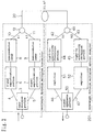
- Figure 1 is a block diagram of the optical transmission system according to the embodiment.
- the optical transmission system comprises a wavelength division multiplex optical transmitter 1, an optical fiber 20, and a wavelength division multiplex optical receiver 2.
- the wavelength division multiplex optical transmitter 1 comprises a band division portion 3, signal amplification portions 6 and 7, semiconductor lasers 8 and 9 for performing electricity-to-light conversion, and an optical multiplex portion 12.
- An optical signal from the wavelength division multiplex optical transmitter 1 is transmitted through the optical fiber 20 and input into the wavelength division multiplex optical receiver 2.
- the semiconductor lasers 8 and 9 correspond to the electricity-to-light conversion means according to the invention.
- the wavelength division multiplex optical receiver 2 comprises an optical branch portion 31, light-to-electricity conversion portions 34 and 35, amplifiers 36 and 37, and a signal synthesis portion 50.
- the light-to-electricity conversion portions 34 and 35 each have a photodetector having electrical output means. Further, a matching circuit having the function of a low pass filter is inserted in the electrical output means of the light-to-electricity conversion means 34, and a matching circuit having the function of a band pass filter is inserted in the electrical output means of the light-to-electricity conversion portion 35.
- the means including the light-to-electricity conversion portions 34 and 35 corresponds to the means including the light-to-electricity conversion means and filter means according to the invention.
- the means including the matching circuit according to the embodiment corresponds to the filter means according to the invention.
- Figure 7 shows a frequency arrangement diagram of a signal group to be transmitted.
- an electrical signals obtained by frequency multiplexing of the sub-carriers having each of the frequencies f1 to f4 is input into the wavelength division multiplex optical transmitter 1.
- This input electrical signal is divided by the band division portion 3 into a signal group 3000 having a frequency band f1 to f2 and a signal group 3001 having a frequency band f3 to f4.
- the signal group 3000 is input into the signal amplification portion 6 via a path 4, and converted into an optical signal having a wavelength ⁇ 1 by the semiconductor laser 8, and then the optical signal is output into an optical fiber 10.
- the signal group 3002 is amplified in the signal amplification portion 7 via a path 5 and converted into an optical signal having a wavelength ⁇ 2 different from the wavelength ⁇ 1, by the semiconductor laser 9 and then the optical signal is output into an optical fiber 11.
- the optical signals of the wavelengths ⁇ 1 and ⁇ 2 are wavelength-multiplexed in the optical multiplex portion 12, and then transmitted from the wavelength division multiplex optical transmitter 1 through the optical fiber 20.
- the transmitted optical signal is input into the wavelength division multiplex optical receiver 2, in which it is branched by the optical branch portion 31, and then the branched optical signals are introduced into optical fibers 32 and 33, respectively.
- the optical signal introduced into the optical fiber 32 and the optical signal introduced into the optical fiber 33 are identical optical signals.
- the optical signal introduced into the optical fiber 32 is converted into an electrical signal by the light-to-electricity conversion portion 34.
- This light-to-electricity conversion portion 34 has response only to the frequency band f1 to f2 of the signal group 3000 due to the above described function of a low pass filter.
- the optical signal introduced into the optical fiber 32 is converted into the signal group 3000 having the frequency band from f1 to f2, and the signal group 3000 is amplified by the amplifier 36 and introduced into a path 38.
- the optical signal introduced into the optical fiber 33 is converted into an electrical signal by the light-to-electricity conversion portion 35.
- This light-to-electricity conversion portion 35 has response only to the frequency band f3 to f4 of the signal group 3001 due to the above described function of a band pass filter.
- the optical signal introduced into the fiber 33 is converted into the signal group 3001 having the frequency band f3 to f4, and the signal group 3001 is amplified by the amplifier 37 and introduced into a pass 39.
- a signal to be sent is divided into more than two frequency bands, and (1) by decreasing the number of sub-carriers in each of the frequency bands, the above described intermodulation distortion in each of the frequency bands can be reduced, and further (2) by converting the above divided signals into optical signals of different wavelengths for each of the frequency bands and optically transmitting the optical signals, no intermodulation distortion is generated between each of the frequency bands, allowing the sending of optical signals of low-distortion.
- both second-order intermodulation distortion and third-order intermodulation distortion are reduced in each of the frequency bands.
- the semiconductor laser 8 of this embodiment have only to convert signals of the lower frequency band to optical signals, allowing the use of low-cost semiconductor lasers of which broad band response is not required (for example, a coaxial type or surface-mount type module).
- the electrical output means of the photodetector constituting the light-to-electricity conversion portion which output means includes an inserted matching circuit having a low pass filter on the lower frequency side and a band pass filter function including a pass band on the high frequency side, for example,.
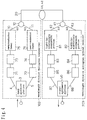
- Figure 2 is a block diagram of the optical transmission system according to the embodiment.
- optical transmission system according to the embodiment is different from the embodiment 1 described above primarily from the following two points of view.
- a demultiplex portion 41 performs wavelength separation of the optical signal into light beams of a wavelength ⁇ 1 and a wavelength ⁇ 2, and the light beams are introduced into optical fibers 42 and 43, respectively;
- the optical signal of the wavelength ⁇ 1 is converted into an electrical signal of the group 3000 in a light-to-electricity conversion portion 44, and the electrical signal is introduced into a path 46 via an amplifier 51.
- the optical signal of the wavelength ⁇ 2 is converted into an electrical signal of the signal group 3001 in a light-to-electricity conversion portion 45, and the electrical signal is introduced into a path 47 via an amplifier 52.
- the means including the light-to-electricity conversion portions 44 and 45 corresponds to the light-to-electricity conversion means according to the invention.
- the wavelength-multiplexed light beam is subjected to wavelength separation, and each of the wavelength-separated light beams is converted from light to electricity.
- no intermodulation distortion between signal groups is generated in the light-to-electricity conversion portion, thus allowing transmission of lower distortion together with the wavelength division multiplex optical transmitter.
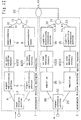
- Figure 3 is a block diagram of the optical transmission system according to the embodiment.
- the configuration of the optical transmission system according to the present embodiment is different from the optical transmission system according to the embodiments 1 and 2 described above primarily from the following two points of view.
- the two points are as follows; (1) in a wavelength division multiplex optical transmitter 101, the total modulation degree in converting of an electrical signal into an optical signal by a signal amplification portion 61 and a semiconductor laser 63 and the total modulation degree in converting of an electrical signal into an optical signal by a signal amplification portion 62 and a semiconductor laser 64 can be made different from each other depending on the transmission quality required from the signals divided into bands by a band division portion 3, and (2) in an wavelength division multiplex optical receiver 202, the total light-to-electricity conversion efficiency by a light-to-electricity conversion portion 44 and an amplifier 65 and the light-to-electricity conversion efficiency by a light-to-electricity conversion portion 45 and an amplifier 66 can be made different from each other depending on signal components (e.g. amplitude) of the light beam of each wavelength transmitted from the wavelength division multiplex optical transmission portion.
- signal components e.g. amplitude
- the signal group 3000 is made up of an analog-modulated signal group and the signal group 3001 is made up of a digitally modulated signal group.
- the wavelength division multiplex optical transmitter 101 (1) sets the semiconductor laser 63 such that the optical modulation degree of an optical signal of wavelength ⁇ 1 for transmitting the signal group 3000 may be an optical modulation degree suitable for analog modulation (i.e. an optical modulation degree not generating nonlinear distortion during modulation (percentage optical-modulation of 35% or less ) ) , and (2) increases the output light intensity level by increasing the current value of a bias current of the semiconductor 63 and adjusting the intensity of the electrical signal by the signal amplification portion 61.
- an optical modulation degree suitable for analog modulation i.e. an optical modulation degree not generating nonlinear distortion during modulation (percentage optical-modulation of 35% or less )
- increases the output light intensity level by increasing the current value of a bias current of the semiconductor 63 and adjusting the intensity of the electrical signal by the signal amplification portion 61.
- the reason for increasing the current value of the bias current of the semiconductor laser 63 is because the output light intensity level (average output light intensity level in the embodiment) of the semiconductor laser 63 is determined not by the intensity of the electrical signal to be modulated (an AC signal in the embodiment) , but by the current value of the bias current provided as a bias.
- the sending and receiving should be performed at a high output light intensity level in order to ensure a predetermined value of C/N.
- the wavelength division multiplex optical transmitter 101 sets the percentage optical-modulation of the optical signal of wavelength ⁇ 2 transmitting the signal group 3001 to about 100% by the semiconductor laser 64 in order to increase extinction ratio.
- a total optical modulation degree in converting an electrical signal into an optical signal is adjusted in this manner, and the optical beams having these wavelengths ⁇ 1 and ⁇ 2 are wavelength-multiplexed in an optical multiplex portion 12, and then transmitted.
- the wavelength division multiplex optical receiver 202 performs the light-to-electricity converting of an optical signal subjected to wavelength separation in wavelength separation portion 41, the analog optical signal (wavelength ⁇ 1) is converted into an electrical signal by the light-to-electricity conversion portion 44 and the amplifier 65 and the digital optical signal (wavelength ⁇ 2) is converted into an electrical signal by the light-to-electricity conversion portion 45 and the amplifier 66, respectively.
- the total light-to-electricity conversion efficiency of each signal path is adjusted such that the level deviation between the respective signal groups may be the same as the original signals.
- the light beam sending side adjusts the optical modulation degree and output optical intensity and the light beam receiving side adjusts the light-to-electricity conversion efficiency, so that a transmission system for satisfying signal transmission quality for each signal can be constructed.
- the embodiment is not limited to this case but can be applicable to signal groups having a difference in predetermined C/N values therefor.
- the intensity of electrical signals of a plurality of frequency bands according to the invention is determined such that the light intensity of the analog-modulated electrical signal may be increased during sending and receiving of light.
- the embodiment is not limited to this, but the intensity of the electrical signals of a plurality of frequency bands according to the invention can be set, for example, such that the light intensity for the electrical signal having a larger predetermined value of C/N may be increased during sending and receiving of light.
- the intensity of electrical signals of a plurality of frequency bands according to the invention can be different based on the properties of electrical signals and/or optical signals.
- the optical modulation degrees of optical signals of converted different wavelengths according to the invention is determined such that the optical modulation degree of the analog-modulatedoptical signal may be small not to generate non-linear distortion, and such that the optical modulation degree of the digitally modulated optical signal may be about 100%.
- the embodiment is not limited to this, but, briefly speaking, the optical modulation degrees of the optical signals of converted wavelengths different from each other according to the invention can be different based on the properties of the electrical signals and/or the optical signals.
- both of the intensity of electrical signals of a plurality of frequency bands and the optical modulation degrees of the optical signals of converted different wavelengths according to the invention are different based on the electrical signals and/or the optical signals.
- the embodiment is not limited to this, but at least one of the intensity of electrical signals of a plurality of frequency bands and the optical modulation degrees of the optical signals of converted different wavelengths according to the invention can be different based on the properties of the electrical signals and/or the optical signals.
- the total light-to-electricity conversion efficiency is adjusted such that the level deviation between each of the signal groups may be the same as the original signal.
- the embodiment is not limited to this, but in respectively reconstructing the electrical signals of a plurality of frequency bands from the optical signals from the wavelength division multiplex optical transmitter according to the invention, briefly speaking, it is sufficient to consider the intensity of the electrical signals of a plurality of frequency bands and/or the optical modulation degrees of the optical signals of converted different wavelengths, which intensity and optical modulation degrees each are different based on the properties of the electrical signals and/or optical signals.
- Figure 4 is a block diagram of the optical transmission system according to the present embodiment
- Figure 8 shows a frequency arrangement diagram of an FM converted signal.
- the configuration of the optical transmission system according to the embodiment comprises FM modulation portions 71 and 72 and FM demodulation portions 85 and 86, in the points of which the present embodiment is different from the optical transmission system according to the embodiment 2 described above.
- One signal group 3000 divided by the band division portion 3 of the wavelength division multiplex optical transmitter 102 is input into the FM modulation portion 71 via a path 4 and FM converted therein.
- the FM converted signal becomes a signal 3004 centered at an FM carrier frequency fL as shown in Figure 8, and the signal 3004 is input into a semiconductor laser 75 via a band pass filter 73, generating an optical signal of wavelength ⁇ 1.
- another signal group 3001 having its band divided is FM converted in an FM modulation portion 72 via a path 5.
- the FM converted signal becomes a signal 3005 centered at an FM carrier frequency fH as shown in Figure 8, and the signal 3005 is input into a semiconductor laser 76 via a band pass filter 74, generating an optical signal of wavelength ⁇ 2.
- the band pass filters 73 and 74 is to remove unwanted spectra generated in the side bands of the signals 3004 and 3005 (see Figure 8), which spectra may cause spurious output on the receiving side.
- the FM modulation portions 71 and 72 can perform FM conversion with sufficiently high accuracy, few unwanted spectra as described above are generated, and therefore the band pass filters 73 and 74 become unnecessary.
- the optical signals of these two different wavelengths are wavelength-multiplexed in the optical multiplex portion 12 to be transmitted through the optical fiber 20.
- the transmitted wavelength-multiplexed light beam is input into a wavelength division multiplex optical receiver 203, and subjected to wavelength separation in an optical multiplex portion 41.
- the optical signal of wavelength ⁇ 1 passes through an optical fiber 42 and is converted into an electrical signal in a light-to-electricity conversion portion 81. Then, the electrical signal is demodulated into the signal group 3000 in an FM demodulation portion 85 after signal amplification by an amplifier 83.
- the optical signal of wavelength ⁇ 2 passes through an optical fiber 43 and is converted into an electrical signal in a light-to-electricity conversion portion 82. Then, the electrical signal is demodulated into the signal group 3001 in an FM demodulation portion 86 after signal amplification by an amplifier 84. These two demodulated signals are synthesized in a signal synthesis portion 50, and taken out as the original signal.
- FM modulation portion and FM demodulation portion can reduce signal-quality degradation caused by light beams reflected back during transmitting through an optical fiber.
- the present embodiment uses two FM carrier frequencies fL and fH different from each other, the use of wavelength division multiplex transmission would provide no limit on the setting of carrier frequencies because FM carriers of different wavelengths do not cause interference with each other.
- FM carrier frequencies of FM signals are desirably set such that their signal-occupied bands may not overlap with each other.
- FM carrier frequencies are variable, by resetting FM carrier frequencies so as to minimize possible distortion generated during FM demodulation, the optical signal transmission of better quality can be maintained.
- the present embodiment performs FM conversion in each of signal paths, it is possible to configure at least one of the paths for use in FM conversion.
- a certain signal group is analog signals requiring high transmission quality
- FM conversion is used for the signal group
- the other signal group is digital signals not requiring so high transmission quality
- a desired quality may be still satisfied by converting the other signal group, without FM conversion, into an optical signal for optical transmission.
- the FM modulation portion for example a voltage-controlled oscillator can be used.
- the voltage-controlled oscillator can be an oscillator using a varactor or a reactance transistor and a digital oscillator using a multivibrator.
- the configuration of the FM demodulation portion is desirably of a delay line type or pulse count type having a broad band and good linearity, though there are a number of configurations of the FM demodulation portion.
- it is two output elements and AND elements which are high speed digital elements, and elements using delay circuits (not shown).
- the configuration of the FM demodulation portion is not limited to the above described configurations , and itmaybe a circuithaving the function of frequency discrimination, such as a double tuned frequency discriminator, a Foster-Seeley discriminator and a ratio detector.
- Figure 5 is a block diagram of the optical transmission system according to the embodiment.
- optical transmission system according to the embodiment is different from the embodiment 2 described above primarily from the following two points of view.
- the signal group 3001 has its signal band shifted to the lower frequency side in a frequency conversion portion 90 of a wavelength division multiplex optical transmitter 103, and then is converted into an optical signal of wavelength ⁇ 2 by a semiconductor laser 92 via a signal amplification portion 91, and (2) an optical signal of wavelength ⁇ 2 obtained by wavelength separation in the optical demultiplex portion 41 of a wavelength division multiplex optical receiver 204 is converted into an electrical signal in a light-to-electricity conversion portion 94, which electrical signal is shifted, .in the direction opposite to the previous shift, to the frequency band of the original signal group 3001 in a frequency conversion portion 95 and input into a signal synthesis portion 50 via an amplifier 97, and then output as the original signal therefrom.
- the frequency conversion portion 95 corresponds to the frequency conversion means according to the invention.
- the optical transmission system of the embodiment by shifting the signal of a high frequency region to the lower frequency side, not only the frequency response required of the semiconductor laser can be eased in the high frequency region, but also the required frequency response of the photodetector of the light-to-electricity conversion portion can be eased in the high frequency region.
- the optical transmission device of low cost can be used, and also the apparatus can be made low cost.
- Figure 6 is a block diagram of the optical transmission system according to the embodiment.
- optical transmission system according to the embodiment is different from the embodiment 5 described above primarily from the following two points of views.
- a frequency conversion portion 111 of a wavelength division multiplex optical transmitter 104 provides, from a signal generation portion 112, a reference frequency for frequency-shifting of the signal group 3001, and the reference frequency signal is converted into an optical signal of a different wavelength ⁇ 3 by a semiconductor laser 116, and the optical signal is wavelength-multiplexed together with the signals of wavelengths ⁇ 1 and ⁇ 2 in an optical multiplex portion 120 to be transmitted therefrom, and (2) an optical demultiplex portion 130 of a wavelength division multiplex optical receiver 205 performs wavelength separation of the above described optical signals, which have been wavelength-multiplexed in the optical multiplex portion 120, into optical signals having wavelengths ⁇ 1 to ⁇ 3, among which the optical signal of wavelength ⁇ 3 is converted into an reference frequency signal in a light-to-electricity conversion portion 136 via an optical fiber 133, which reference frequency signal is , via an amplifier 138, took into a frequency conversion portion 137 to be used as a reference signal for frequency-shifting of the signal obtained by
- the light-to-electricity conversion portion 136 corresponds to the light-to-electricity conversion means according to the invention.
- the frequency conversion portion 137 corresponds to the frequency conversion means according to the invention.
- a reference frequency signal on the sending side can be used on the receiving side as it is, not only the accuracy of frequency shift is improved, but also even the change of the reference frequency on the sending side is detected in real time on the receiving side, allowing an accurate shift of frequency to be performed.
- the frequency conversion according to the invention is performed by a shift toward the lower frequency side in the embodiment described above.
- the frequency conversion according to the invention can be performed by shifting toward the higher frequency side, for example, when the wavelength division multiplex optical receiver exhibit better response in a band of the high frequency region.
- the frequency conversion according to the invention can be performed by shifting at least one frequency band of a plurality of frequency bands toward the higher frequency side or toward the lower frequency side.
- frequency conversion means of performing a shift in the direction opposite to this shift is necessary on the receiving side.
- Figure 9 is a block diagram of the optical transmission system according to the embodiment.
- An optical transmission device 500 comprises a wavelength division multiplex optical transmitter 501, an output fiber 503, a wavelength division multiplex optical receiver 502, and an input fiber 504. Also, an optical transmission device 510 comprises a wavelength division multiplex optical transmitter 509, an output fiber 507, a wavelength division multiplex optical receiver 508, and an input fiber 505.
- the output fiber 503 and the input fiber 504 are connected to an optical fiber 505 through an optical multiplex and demultiplex portion 511. Also, the output fiber 507 and the input fiber 506 are connected to the optical fiber 505 through an optical multiplex and demultiplex portion 512.
- the wavelength range of optical signals output from the wavelength division multiplex optical transmitter 501 is a 1.3 ⁇ m range
- the wavelength range of optical signals output from the wavelength division multiplex optical transmitter 509 is a 1.5 ⁇ m range.
- wavelength division multiplex optical transmitter and the wavelength division multiplex optical receiver according to the embodiment are, for example, the wavelength division multiplex optical transmitter and the wavelength division multiplex optical receiver that have been described in the above described embodiments 1 to 6.
- a signal group input into the wavelength division multiplex optical transmitter 501 is converted into a wavelength-multiplexed optical signal of the 1.3 ⁇ m range, which is input into the optical multiplex and demultiplex portion 511 through the optical fiber 503 and then transmitted through the optical fiber 505.
- the optical signal transmitted from the side of the optical transmission device 500 passes through the optical fiber 506 from the optical multiplex and demultiplex portion 512 to be input into the side of the optical transmission device 510, and then is took out as the original signal group in the wave length division multiplex optical receiver 508.
- a signal group input into the wavelength division multiplex optical transmitter 509 is converted into a wavelength-multiplexed optical signal of the 1.5 ⁇ m range, which is input into the optical multiplex and demultiplex portion 512 through the optical fiber 507 and then transmitted through the optical fiber 505.
- the optical signal transmitted from the side of the optical transmission device 510 passes through the optical fiber 504 from the optical multiplex and demultiplex portion 511 to be input into the side of the optical transmission device 500, and then is took out as the original signal group by the wavelength division multiplex optical receiver 502.
- any optical device which is capable of synthesis and separation of the light beam of the 1.3 ⁇ m range and the light beam of the 1.5 ⁇ m range can be used for the optical multiplex and demultiplex portions 511 and 512.
- the optical transmission device comprises one each of the wavelength division multiplex optical transmitter and the wavelength division multiplex optical receiver in the present embodiment described above, the embodiment is not limited to this, but the optical transmission device may comprise a plurality of the wavelength division multiplex optical transmitters and wavelength division multiplex optical receivers respectively.
- the optical transmission device comprises a plurality of the wavelength division multiplex optical transmitters and wavelength division multiplex optical receivers, for example, a 1.4 ⁇ m range and a 1.6 ⁇ m range can be used as the new wavelength range of optical signals . In this way, transmission capacity can be easily increased.
- long wavelength lasers of In P based materials having a wavelength range of 1.2 - 1.6 ⁇ m, semiconductor lasers of a 0.98 ⁇ m range, lasers of GaAlAs based materials having oscillation wavelength of a 0.78 ⁇ m range can be used.
- optical fiber for example, general optical fibers can be used. These include the general optical fibers of a core diameter of 10 - 300 ⁇ m, for example. By the way, any of the multi-mode optical fibers and the single-mode optical fibers is available.
- the number of band division is 2 and the number of wavelengths for multiplex transmission is 2 or 3 in the present embodiment described above, the embodiment is not limited to this. Briefly speaking, the number of signal bands to be divided is not limited. Also, the number of wavelengths is not limited as far as it is within the transmittable range of the optical fiber, provided the wavelengths are different from each other and wavelength interval between them is ensured to such an extent that disturbance such as interference may not occur (for example, 0.2 nm or more, or uneven intervals).
- the above described embodiment explains the case where the output fiber 503 (507) and the input fiber 504 (506) are connected to the optical fiber 505 by the optical multiplex and demultiplex portion 511 (512), for example.
- the embodiment is not limited this, for example, a three-terminal circulator for use in optical signals can be used instead of the optical multiplex and demultiplex 511 (512).
- an amplifier is provided in the present embodiment described above, it is unnecessary to insert an amplifier when enough signal levels can be ensured.
- the invention provides, for example, a wavelength division multiplex optical transmitter which comprises a signal input portion into which signals using a single sub-carrier or a plurality of signals multiplexed with a plurality of sub-carriers are input, a band division portion for dividing or branching the above described plurality of signals into at least two frequency bands, a plurality of electricity-to-light conversion portions for converting the signals of the plurality of divided frequency bands into light beams each having a wavelength different from each other, and an optical multiplex portion for multiplexing the light beams of mutually different wavelengths from the above described plurality of electricity-to-light conversion portions to output as a wavelength-multiplexed light beam.
- the invention can be configured so as to convert respectively the signals of a plurality of the divided bands into a plurality of FM signals using a plurality of FM conversion portions.
- the invention can be configured so as to have a frequency conversion portion sifting signal bands for at least one of the divided signals.
- the invention provides, for example, a light detection portion for receiving a wavelength-multiplexed light beam from the wavelength division multiplex optical transmitter described above to perform light-to-electricity conversion thereof, and a wavelength division multiplex optical receiver for dividing the electrical signals from the above described light detection portion into at least two frequency bands which do not overlap with each other.
- the invention can be configured with the wavelength division multiplex optical receiver characterized by an optical demultiplex portion for performing wavelength-separation of a wavelength-multiplexed light beam from the wavelength division multiplex optical transmitter into at least two light beams of a plurality of different wavelengths, and by converting the above described light beams of the plurality of wavelengths into electrical signals by a plurality of light detection portions performing light-to-electricity conversion and outputting the electrical signals.
- the configuration according to the invention can have a signal synthesis portion for synthesizing and multiplexing of the electrical signals from the above described plurality of photodetectors.
- the wavelength division multiplex optical receiver receives an FM signal as a input signal, it has an FM demodulation portion for demodulating the FM signal from the photodetector.
- the configuration according to the invention may also comprise a optical branch portion for branching a input light beam into a plurality of light beams and a plurality of light detection portions, into which the light beams branched into plurality are input.
- the plurality of light detection portions may also have different response bands.
- the configuration according to the invention may also comprise at least one frequency conversion portion for performing frequency conversion of the electrical signals from the plurality of light detection portions.
- the configuration according to the invention can be configured such that a reference frequency signal obtained by wavelength separation and light-to-electricity conversion of a wavelength-multiplexed light beam, optically transmitted from the wavelength division multiplex optical transmitter, may be used as a reference frequency signal for frequency conversion.
- the invention relates to, for example, an optical transmission device characterized by comprising the wavelength division multiplex optical transmitter and at least one wavelength division multiplex optical receiver.
- the invention provides an optical transmission system characterized by comprising the wavelength division multiplex optical transmitter described above, an optical transmission line for transmitting light from the wavelength division multiplex optical transmitter, and at least one optical receiver for receiving light transmitted through the above described optical transmission line.
- the invention provides an optical transmission system characterized by comprising at least two optical transmission devices described above, wherein the input and output of each of the above described optical transmission devices are coupled to each other by one optical transmission line having an optical multiplex portion and an optical separation portion and optical signals are bidirectionally transmitted through the optical transmission line.
- the signal bands are divided and the divided bands each are multiplexed and transmitted with each light of a different wavelength, which each light is converted into electrical signals after wavelength separation and then the electrical signals are synthesized. For this reason, because no intermodulation occurs between the signals of the respective wavelength-multiplexed light beams during transmission, it is possible to suppress intermodulation distortion generated in the signal band after receiving and synthesizing when compared to the case where the whole of the signal band is transmitted.
- the division of a signal band into a plurality of frequency bands according to the invention is performed into a frequency band (f1 to f2) located on the lower frequency side and a frequency band (f3 to f4) located on the higher frequency side.
- the division into a plurality of frequency bands according to the invention may be performed into frequency bands (f1 to f5, f6 to f4) located in both end portions and frequency bands (f5 to f2, f3 to f6) located in central portion (f1 ⁇ f5 ⁇ f2, f3 ⁇ f6 ⁇ f4).
- the wavelength division multiplex optical receiver according to the invention comprises a signal synthesis portion 50.
- the wavelength division multiplex optical receiver according to the invention need not comprise signal synthesis means of synthesizing and multiplexing electrical signals of a plurality of frequency bands respectively reconstructed.
- the wavelength division multiplex transmitter according to the invention is described for the case where the semiconductor lasers 8 and 9 are connected to the output sides of the signal amplification portions 6 and 7.
- the wavelength division multiplex optical transmitter according to the invention may be configured such that no loss matching circuits 4000 and 4001 band-matched with the signal bands of electrical signals divided into bands may be inserted between signal amplification portions 6' and 7' and the semiconductor lasers 8 and 9.
- no loss matching circuit 4001 may be inserted at least on the high frequency band side.
- This allows electrical gain to be higher at least on the high frequency band side, and thus the load of the signal amplification portion 7 can be reduced on the higher band side by that amount. That is, it becomes possible to reduce the power consumption and parts count of the signal amplification portion 7.
- no loss matching circuit 4000 is inserted in the path of the low frequency band side, it becomes also possible to reduce the power consumption and parts count of the signal amplification portion 6.
- the wavelength division multiplex receiver according to the invention is described for the case where the amplifiers 36 and 37 are connected to the output sides of the light-to-electricity conversion portions 34 and 35.
- the wavelength division multiplex receiver according to the invention may be configured such that no loss matching circuits 4002 and 4003 band-matched with the signal bands of electrical signals divided into bands may be inserted between the light-to-electricity conversion portions 34 and 35 and the amplifiers 36 and 37, for example as shown in Figure 12.
- no loss matching circuit 4003 may be inserted at least on the high frequency band side.
- This allows electrical gain to be higher at least on the high frequency band side, and thus the load of the signal amplification portion 37 can be reduced on the high frequency band side by that amount. That is, it becomes possible to reduce the power consumption and parts count of the signal amplification portion 37.
- no loss matching circuit 4002 is also inserted in the path of the low frequency band side, it becomes also possible to reduce the power consumption and parts count of the signal amplification portion 36.
- the wavelength division multiplex receiver according to the invention is described for the case where the amplifiers 51 and 52 are connected to the output sides of the light-to-electricity conversion portions 44 and 45.
- the wavelength division multiplex receiver according to the invention may be configured such that no loss matching circuits 4102 and 4103 band-matched with the signal bands of electrical signals divided into bands may be inserted between the light-to-electricity conversion portions 44 and 45 and the amplifiers 51 and 52, as shown in Figure 13 as another example of the wavelength division multiplex optical receiver.
- no loss matching circuit 4103 may be inserted at least on the high frequency band side. This allows electrical gain to be higher at least on the high frequency band side in the same manner as described above, and thus the load of the amplifier 52 can be reduced on the high frequency band side by that amount. Further, when no loss matching circuit 4102 is also inserted in the path of the low frequency band side, it becomes also possible to reduce the power consumption and parts count of the amplifier 51.
- the invention has the advantage that the quality of signals to be optically transmitted can be made better than conventional quality with a simple configuration.
Landscapes
- Engineering & Computer Science (AREA)
- Computer Networks & Wireless Communication (AREA)
- Signal Processing (AREA)
- Optical Communication System (AREA)
Applications Claiming Priority (2)
| Application Number | Priority Date | Filing Date | Title |
|---|---|---|---|
| JP2000279848 | 2000-09-14 | ||
| JP2000279848 | 2000-09-14 |
Publications (2)
| Publication Number | Publication Date |
|---|---|
| EP1189376A2 true EP1189376A2 (de) | 2002-03-20 |
| EP1189376A3 EP1189376A3 (de) | 2005-08-17 |
Family
ID=18764793
Family Applications (1)
| Application Number | Title | Priority Date | Filing Date |
|---|---|---|---|
| EP01122020A Withdrawn EP1189376A3 (de) | 2000-09-14 | 2001-09-13 | Optischer Wellenlängenmultiplex-Sender, optischer Wellenlängenmultiplex-Empfänger, optische Übertragungsvorrichtung, und optisches Übertragungssystem |
Country Status (2)
| Country | Link |
|---|---|
| US (1) | US20020075539A1 (de) |
| EP (1) | EP1189376A3 (de) |
Cited By (2)
| Publication number | Priority date | Publication date | Assignee | Title |
|---|---|---|---|---|
| GB2420037A (en) * | 2004-11-05 | 2006-05-10 | Agilent Technologies Inc | Optical transceiver with multiplexed electrical input |
| GB2420036A (en) * | 2004-11-05 | 2006-05-10 | Agilent Technologies Inc | Optical transceiver with a composite electrical input |
Families Citing this family (9)
| Publication number | Priority date | Publication date | Assignee | Title |
|---|---|---|---|---|
| US7603037B2 (en) * | 2003-06-20 | 2009-10-13 | Hrl Laboratories, Llc | Ultra-dense wavelength and subcarrier multiplexed optical and RF/mm-wave transmission system |
| US20050089330A1 (en) * | 2003-10-23 | 2005-04-28 | Grot Annette C. | Optical communication network |
| JPWO2005088877A1 (ja) * | 2004-03-10 | 2008-01-31 | 松下電器産業株式会社 | 光送信装置および光伝送システム |
| SE1200578A1 (sv) * | 2012-09-26 | 2014-03-27 | Deltanode Solutions Ab | Distributionsnät för ett distribuerat antennsystem |
| US10353194B2 (en) | 2016-12-29 | 2019-07-16 | Booz Allen Hamilton Inc. | M-ary frequency presence modulation communication system and method |
| US10256916B2 (en) * | 2016-12-29 | 2019-04-09 | Booz Allen Hamilton Inc. | M-ARY frequency presence modulation communication system and method |
| US10897264B2 (en) | 2019-06-24 | 2021-01-19 | Booz Allen Hamilton Inc. | Data receiver for communication system |
| JP7008884B2 (ja) * | 2019-10-01 | 2022-02-10 | 三菱電機株式会社 | 送受信装置及び送受信方法 |
| CN114422032A (zh) * | 2021-12-20 | 2022-04-29 | 中航光电科技股份有限公司 | 一种适用于舰载电子战系统的多路射频光传输设备 |
Family Cites Families (3)
| Publication number | Priority date | Publication date | Assignee | Title |
|---|---|---|---|---|
| DE3010802A1 (de) * | 1980-03-20 | 1981-09-24 | Siemens AG, 1000 Berlin und 8000 München | Schaltungsanordnung zur multiplexuebertragung mehrerer nachrichtenbaender |
| DE3203785A1 (de) * | 1982-02-04 | 1983-08-11 | AEG-Telefunken Nachrichtentechnik GmbH, 7150 Backnang | Verfahren zur analogen uebertragung und verteilung von mehrkanal-frequenzmultiplex-signalen ueber lichtwellenleiter |
| DE4001039A1 (de) * | 1990-01-16 | 1991-07-18 | Standard Elektrik Lorenz Ag | Optisches kabelfernseh-uebertragungssystem |
-
2001
- 2001-09-13 EP EP01122020A patent/EP1189376A3/de not_active Withdrawn
- 2001-09-14 US US09/952,072 patent/US20020075539A1/en not_active Abandoned
Cited By (2)
| Publication number | Priority date | Publication date | Assignee | Title |
|---|---|---|---|---|
| GB2420037A (en) * | 2004-11-05 | 2006-05-10 | Agilent Technologies Inc | Optical transceiver with multiplexed electrical input |
| GB2420036A (en) * | 2004-11-05 | 2006-05-10 | Agilent Technologies Inc | Optical transceiver with a composite electrical input |
Also Published As
| Publication number | Publication date |
|---|---|
| US20020075539A1 (en) | 2002-06-20 |
| EP1189376A3 (de) | 2005-08-17 |
Similar Documents
| Publication | Publication Date | Title |
|---|---|---|
| US5212579A (en) | Method and apparatus for communicating amplitude modulated signals over an optical communication path | |
| JP4184474B2 (ja) | 光伝送システムならびにそれに用いられる光送信装置および光受信装置 | |
| US5771111A (en) | Optical network | |
| JPH11331089A5 (de) | ||
| US6788169B1 (en) | Amplifier composite triple beat (CTB) reduction by phase filtering | |
| US7376356B2 (en) | Optical data transmission system using sub-band multiplexing | |
| US6147784A (en) | Simultaneous wavelength-division multiplexing and broadcast transmission system | |
| EP1189376A2 (de) | Optischer Wellenlängenmultiplex-Sender, optischer Wellenlängenmultiplex-Empfänger, optische Übertragungsvorrichtung, und optisches Übertragungssystem | |
| US5896216A (en) | AM/PM converter and optical signal transmission system | |
| EP0168914A1 (de) | Optisches Übertragungssystem | |
| JP3970303B2 (ja) | 光信号送信機 | |
| WO2005027380A1 (ja) | 光信号受信機、光信号受信装置及び光信号伝送システム | |
| US6452706B1 (en) | FM signal optical transmission apparatus and FM signal optical reception apparatus | |
| JP3371355B2 (ja) | 変調方式変換回路及び光信号伝送装置 | |
| US8682166B2 (en) | Subcarrier multiplexing type optical communication method and passive optical network using the same | |
| JP2002164868A (ja) | 波長多重光送信器、波長多重光受信器、光伝送装置、および光伝送システム | |
| JPH08274714A (ja) | 光信号送信機 | |
| JP2001183711A (ja) | 光周波数変換装置および方法 | |
| JP7258243B1 (ja) | 光受信装置 | |
| JP4374011B2 (ja) | 光信号送信機及び光信号伝送システム | |
| JPH0454034A (ja) | サブキャリア多重光伝送方法およびサブキャリア多重光伝送装置 | |
| JP2000349560A (ja) | 電圧制御発振器、fm信号光送信器、fm信号光受信器及びfm信号光伝送システム | |
| JP2004040242A (ja) | 信号伝送方法および信号伝送システム | |
| JP2743911B2 (ja) | 光ヘテロダイン型fm変調装置 | |
| JP3782599B2 (ja) | Fm信号光伝送装置 |
Legal Events
| Date | Code | Title | Description |
|---|---|---|---|
| PUAI | Public reference made under article 153(3) epc to a published international application that has entered the european phase |
Free format text: ORIGINAL CODE: 0009012 |
|
| AK | Designated contracting states |
Kind code of ref document: A2 Designated state(s): AT BE CH CY DE DK ES FI FR GB GR IE IT LI LU MC NL PT SE TR |
|
| AX | Request for extension of the european patent |
Free format text: AL;LT;LV;MK;RO;SI |
|
| PUAL | Search report despatched |
Free format text: ORIGINAL CODE: 0009013 |
|
| AK | Designated contracting states |
Kind code of ref document: A3 Designated state(s): AT BE CH CY DE DK ES FI FR GB GR IE IT LI LU MC NL PT SE TR |
|
| AX | Request for extension of the european patent |
Extension state: AL LT LV MK RO SI |
|
| AKX | Designation fees paid | ||
| STAA | Information on the status of an ep patent application or granted ep patent |
Free format text: STATUS: THE APPLICATION IS DEEMED TO BE WITHDRAWN |
|
| 18D | Application deemed to be withdrawn |
Effective date: 20020331 |
|
| REG | Reference to a national code |
Ref country code: DE Ref legal event code: 8566 |