EP1193542A2 - Méthode et dispositif pour imprimer des images monochromes utilisant un modulateur spatial de lumière avec une source de lumière sélectionnable - Google Patents
Méthode et dispositif pour imprimer des images monochromes utilisant un modulateur spatial de lumière avec une source de lumière sélectionnable Download PDFInfo
- Publication number
- EP1193542A2 EP1193542A2 EP01203554A EP01203554A EP1193542A2 EP 1193542 A2 EP1193542 A2 EP 1193542A2 EP 01203554 A EP01203554 A EP 01203554A EP 01203554 A EP01203554 A EP 01203554A EP 1193542 A2 EP1193542 A2 EP 1193542A2
- Authority
- EP
- European Patent Office
- Prior art keywords
- spatial light
- modulator
- light source
- light modulator
- printer
- Prior art date
- Legal status (The legal status is an assumption and is not a legal conclusion. Google has not performed a legal analysis and makes no representation as to the accuracy of the status listed.)
- Withdrawn
Links
- 238000007639 printing Methods 0.000 title claims description 51
- 238000000034 method Methods 0.000 title abstract description 18
- 230000010287 polarization Effects 0.000 claims abstract description 49
- 238000001914 filtration Methods 0.000 claims description 2
- 238000003384 imaging method Methods 0.000 abstract description 22
- 238000005286 illumination Methods 0.000 abstract description 21
- 238000013461 design Methods 0.000 abstract description 9
- 238000002059 diagnostic imaging Methods 0.000 abstract description 4
- 230000003287 optical effect Effects 0.000 description 17
- 230000008901 benefit Effects 0.000 description 13
- 238000005516 engineering process Methods 0.000 description 10
- 230000035945 sensitivity Effects 0.000 description 9
- 238000011161 development Methods 0.000 description 8
- 230000018109 developmental process Effects 0.000 description 8
- 230000000694 effects Effects 0.000 description 8
- 239000004973 liquid crystal related substance Substances 0.000 description 7
- 238000003491 array Methods 0.000 description 6
- 238000003860 storage Methods 0.000 description 6
- 239000002609 medium Substances 0.000 description 5
- 230000004044 response Effects 0.000 description 5
- 239000006059 cover glass Substances 0.000 description 4
- 229910052736 halogen Inorganic materials 0.000 description 4
- 150000002367 halogens Chemical class 0.000 description 4
- 230000006870 function Effects 0.000 description 3
- 230000007246 mechanism Effects 0.000 description 3
- 238000004806 packaging method and process Methods 0.000 description 3
- 230000009467 reduction Effects 0.000 description 3
- 230000004075 alteration Effects 0.000 description 2
- 238000013459 approach Methods 0.000 description 2
- 239000002131 composite material Substances 0.000 description 2
- 230000001419 dependent effect Effects 0.000 description 2
- 230000006872 improvement Effects 0.000 description 2
- 238000004519 manufacturing process Methods 0.000 description 2
- 230000008569 process Effects 0.000 description 2
- 238000012545 processing Methods 0.000 description 2
- 230000009471 action Effects 0.000 description 1
- 230000003213 activating effect Effects 0.000 description 1
- 230000001154 acute effect Effects 0.000 description 1
- 230000032683 aging Effects 0.000 description 1
- 230000003466 anti-cipated effect Effects 0.000 description 1
- 239000012736 aqueous medium Substances 0.000 description 1
- 230000000712 assembly Effects 0.000 description 1
- 238000000429 assembly Methods 0.000 description 1
- 230000008033 biological extinction Effects 0.000 description 1
- 230000001427 coherent effect Effects 0.000 description 1
- 239000003086 colorant Substances 0.000 description 1
- 150000001875 compounds Chemical class 0.000 description 1
- 230000007547 defect Effects 0.000 description 1
- 238000001035 drying Methods 0.000 description 1
- 238000010894 electron beam technology Methods 0.000 description 1
- 239000000839 emulsion Substances 0.000 description 1
- 238000005538 encapsulation Methods 0.000 description 1
- 230000007613 environmental effect Effects 0.000 description 1
- 230000004907 flux Effects 0.000 description 1
- 238000003707 image sharpening Methods 0.000 description 1
- 238000010348 incorporation Methods 0.000 description 1
- 238000003780 insertion Methods 0.000 description 1
- 230000037431 insertion Effects 0.000 description 1
- 230000003993 interaction Effects 0.000 description 1
- 230000007774 longterm Effects 0.000 description 1
- 239000000203 mixture Substances 0.000 description 1
- 230000004048 modification Effects 0.000 description 1
- 238000012986 modification Methods 0.000 description 1
- 239000004065 semiconductor Substances 0.000 description 1
- 238000007493 shaping process Methods 0.000 description 1
- 238000009987 spinning Methods 0.000 description 1
- 239000000126 substance Substances 0.000 description 1
- 238000012546 transfer Methods 0.000 description 1
Images






Classifications
-
- G—PHYSICS
- G03—PHOTOGRAPHY; CINEMATOGRAPHY; ANALOGOUS TECHNIQUES USING WAVES OTHER THAN OPTICAL WAVES; ELECTROGRAPHY; HOLOGRAPHY
- G03B—APPARATUS OR ARRANGEMENTS FOR TAKING PHOTOGRAPHS OR FOR PROJECTING OR VIEWING THEM; APPARATUS OR ARRANGEMENTS EMPLOYING ANALOGOUS TECHNIQUES USING WAVES OTHER THAN OPTICAL WAVES; ACCESSORIES THEREFOR
- G03B27/00—Photographic printing apparatus
- G03B27/72—Controlling or varying light intensity, spectral composition, or exposure time in photographic printing apparatus
Definitions
- This invention relates generally to a method and apparatus for printing monochromatic imaging onto photosensitive media by spatially and temporally modulating a light beam, and more particularly to a film recording apparatus that allows selection of a light source of a preferred wavelength from among a set of available light sources having different wavelengths.
- printers generally adapted to record images provided from digital data onto photosensitive media apply light exposure energy that may originate from a number of different sources and may be modulated in a number of different ways.
- light exposure energy can be applied from a CRT-based printer.
- the digital data is used to modulate a Cathode Ray Tube (CRT) which provides exposure energy by scanning an electron beam of variable intensity along its phosphorescent screen.
- CRT Cathode Ray Tube
- light exposure energy can be applied from a laser-based printer, as is disclosed in U.S. Patent No. 4,728,965 (Kessler, et al.)
- the digital data is used to modulate the duration of laser on-time or intensity as the beam is scanned by a rotating polygon onto the imaging plane.
- CRT- and laser-based printers perform satisfactorily for photoprocessing applications, that is, for printing of photographs for consumer and commercial markets.
- alternative technologies have been considered for use in photoprocessing printers.
- suitable candidate technologies under development are two-dimensional spatial light modulators.
- Two-dimensional spatial light modulators such as those using a digital micromirror device (DMD) from Texas Instruments, Dallas, Texas, or using a liquid crystal device (LCD) can be used to modulate an incoming optical beam for imaging.
- a spatial light modulator can be considered essentially as a two-dimensional array of light-valve elements, each element corresponding to an image pixel. Each array element is separately addressable and digitally controlled to modulate incident light from a light source by modulating the polarization state of the light. Polarization considerations are, therefore, important in the overall design of support optics for a spatial light modulator.
- the first type developed was the transmissive spatial light modulator, which, as its name implies, operates by modulating an optical beam that is transmitted through individual array elements.
- the second type, a later development, is a reflective spatial light modulator.
- the reflective spatial light modulator operates by modulating a reflected optical beam through individual array elements.
- a suitable example of an LCD reflective spatial light modulator relevant to this application utilizes an integrated CMOS backplane, allowing a small footprint and improved uniformity characteristics.
- LCD spatial light modulators have been developed and employed for digital projection systems for image display, such as is disclosed in U.S. Patent No. 5,325,137 (Konno et al.) and in miniaturized image display apparatus suitable for mounting within a helmet or supported by eyeglasses, as is disclosed in U.S. Patent No. 5,808,800 (Handschy et al.) LCD projector and display designs in use typically employ one or more spatial light modulators, such as using one for each of the primary colors, as is disclosed in U.S. Patent No. 5,743,610 (Yajima et al.).
- imaging requirements for projector and display use differ significantly from imaging requirements for printing.
- Projectors are optimized to provide maximum luminous flux to a screen, with secondary emphasis placed on characteristics important in printing, such as contrast and resolution.
- Optical systems for projector and display applications are designed for the response of the human eye, which, when viewing a display, is relatively insensitive to image artifacts and aberrations and to image non-uniformity, since the displayed image is continually refreshed and is viewed from a distance.
- a preferred approach for photoprocessing printers uses an LCD-based spatial light modulator.
- Liquid crystal modulators can be a low cost solution for applications requiring spatial light modulators.
- Photographic printers using commonly available LCD technology are disclosed in U.S. Patent Nos. 5,652,661; 5,701,185 (Reiss et al.); and 5,745,156 (Federico et al.)
- references to LCD in the subsequent description can be generalized, for the most part, to other types of spatial light modulators, such as the DMD noted above.
- spatial light modulators have largely been adapted for continuous tone (contone) color imaging applications. Unlike other digital printing devices, such as the CRT and laser-based devices mentioned above that scan a beam in a two-dimensional pattern, spatial light modulators image one complete frame at a time. Using an LCD, the total exposure duration and overall exposure energy supplied for a frame can be varied as necessary in order to achieve the desired image density and to control media reciprocity characteristics.
- the capability for timing and intensity control of each individual pixel allows an LCD printer to provide grayscale imaging.
- Printing systems for micrographics or Computer-Output-Microfilm (COM) imaging, diagnostic imaging, and other specialized monochrome imaging applications present a number of unique challenges for optical systems.
- images are archived for long-term storage and retrievability.
- microfilm archives for example, are intended to last for hundreds years in some environments. This archival requirement has, in turn, driven a number of related requirements for image quality.
- image reproduction quality for example, one of the key expectations for micrographics applications is that all images stored on archival media will be written as high-contrast black and white images.
- Color film is not used as a medium for COM applications since it degrades much too quickly for archive purposes and is not capable of providing the needed resolution.
- Grayscale representation meanwhile, has not been available for conventional micrographics printers.
- bitonal representation is appropriate for storage of alphanumeric characters and for standard types of line drawings such as those used in engineering and utilities environments, for example.
- exposure energy applied by the printer is either on or off, to create high-contrast images without intermediate levels or grayscale representation.
- micrographics media is designed to provide much higher resolution than conventional dye-based media provides for color photographic imaging.
- micrographics media employs a much smaller AgX grain size in its photosensitive emulsion.
- Optics components for COM systems are correspondingly designed to maximize resolution, more so than with optical components designed for conventional color photoprocessing apparatus.
- linear arrays such as linear light-emitting diode (LED) arrays, for example, as are used in the Model 4800 Document Archive Writer, manufactured by Eastman Kodak Company, Rochester, New York.
- LED linear light-emitting diode
- Another alternative is use of a linear light-valve array, such as is disclosed in U.S. Patent No. 5,030,970 (Rau et al.)
- COM writers continue to be relatively expensive, largely due to the cost of support components and to the complexity of drive electronics. There is a long-felt need to lower cost and reduce size and complexity for COM devices, without sacrificing performance or robustness.
- a well-known shortcoming of conventional COM printers relates to the interdependence between COM printer design and the exposure sensitivity characteristics of a specific photosensitive media type.
- a particular type of COM printer is designed to write only on a single type of COM media.
- a single type of COM media can only be used in a particular type of COM printer.
- the exposure optics of a particular type of COM printer are designed to apply specific levels of exposure energy over a specific range of wavelengths to the COM media. Because of this constraint, a customer who purchases a COM printer of specific manufacture and model type can use that COM printer only with COM media that has been developed specifically for that printer, or with a very limited number of other types of media having similar characteristics. This is true even though the same media handling subsystem used in the COM printer could be capable of routing different types of photosensitive media from a film supply, through an exposure section, and to a film processing or film storage unit for exposed media.
- Exposure wavelength is one important characteristic that constrains COM printer use to a specific media.
- Existing COM printers use monochromatic light as the source of exposure energy.
- Different COM media are designed for optimum performance with monochromatic exposure light at different wavelengths.
- the KODAK Archive Storage Media 3459 is optimized for exposure wavelengths near 685 nm.
- KODAK IMAGELINK DL Microfilm is designed for optimal sensitivity when exposed at 633 nm.
- Conventional exposure optics systems are limited to the use of a single type of exposure light source. Depending on the type of light source used, it can be possible to provide exposure light at different wavelengths. For example, where the exposure light source is a halogen bulb, it would be possible to provide interchangeable filters arranged to allow selection from among multiple exposure wavelengths, depending on the choice of filter. However, such a solution would require manual insertion of a filter element or, if automated, moving parts for positioning a filter in the light path. It could also be possible to provide multiple lasers, for example, and allow an operator-initiated or automated selection of a specific laser in the exposure optics path for a particular COM media.
- an apparatus prints monochrome images from digital image data onto a selected photosensitive medium that is selected from a plurality of photosensitive media compatible with the monochrome printing apparatus.
- a light source which is selectable, selects from a plurality of light source elements a monochromatic light source that is suited to the selected photosensitive medium.
- a uniformizer uniformizes the light that is emitted from the monochromatic light source.
- a polarizer for filtering the uniformized light provides a polarized beam having a predetermined polarization state.
- a spatial light modulator has a plurality of individual elements capable of altering the polarization state of the polarized beam to provide an exposure beam for printing, the state of the elements controlled according to the digital image data.
- a first lens assembly directs the polarized beam to the spatial light modulator and a second lens assembly directs the exposure beam onto the selected photosensitive medium.
- any one of a set of monochromatic light source elements can be selectively energized as the light source for exposing the photosensitive media.
- the monochromatic exposure light is passed through a uniformizer or integrator to provide a source of spatially uniform, monochromatic light for the printing apparatus.
- the monochromatic light is then polarized and passed through a beamsplitter, which directs a polarized beam onto a spatial light modulator.
- Individual array elements of the spatial light modulator, controlled according to digital image data, are turned on or off in order to modulate the polarization rotation of the incident light.
- Modulation for each pixel can be effected by controlling the level of the light from the light source, by control of the drive voltage to each individual pixel in the spatial light modulator, or by controlling the duration of on-time for each individual array element.
- the resulting light is then directed through a lens assembly to expose the photosensitive medium.
- the plurality of monochromatic light sources is made available by the use of an array of LEDs, wherein different groupings of LEDs within the array can be selectively energized to provide optical exposure energy at different wavelengths.
- An advantage of the present invention is that it allows a single monochrome printing apparatus to be able to use a range of media types, where the media types differ in sensitivity to exposure wavelength. This allows an existing printing apparatus to take advantage of new media types as well as improvements in media performance. Conversely, this allows a new printing apparatus to be designed to use both newly introduced and existing media types.
- a further advantage of the present invention is that it allows the development of lower cost photosensitive media by allowing variability over the range of exposure wavelengths used for imaging.
- a further advantage of the present invention is that it can provide wavelength selectivity without introducing any moving part and without appreciably increasing the cost, size, or mechanical complexity of the printer.
- a further advantage of the present invention is that it provides a mechanism for automatically selecting an appropriate light source, based on detecting the type of media loaded in the printing apparatus, thus eliminating operator interaction and possible operator error.
- Figure 1 illustrates an archival printer, such as a COM printer, referred to in general by numeral 100.
- Printer 100 comprises an image forming assembly 10 and a media handling subsystem 212.
- Media handling subsystem 212 comprises a film supply 202, an exposure section 204, an optional film processor 206, and a film storage unit 208.
- a control logic processor 210 accepts and processes image data for printer 100 and controls the overall operation of image forming assembly 10 and media handling subsystem 212 components.
- the operation of printer 100 is straightforward, following the general pattern used for COM printers overall.
- To print an undeveloped section of a photosensitive media 160 is advanced from film supply 202 into exposure section 204.
- Image forming assembly 10 cooperates with control logic processor 210 to print image data onto photosensitive media 160.
- the exposed section of photosensitive media 160 is then ready for processing in order to develop the image.
- film processor 206 may be built into printer 100 itself, as is represented in Figure 1.
- the exposed section of photosensitive media 160 is advanced to film processor 206, where the latent exposed image is developed using a heat process.
- the image development function of film processor 206 is carried out by a separate developing apparatus (not shown), using conventional silver-halide film development chemicals and techniques.
- film storage unit 208 is typically a cassette, designed to keep the exposed photosensitive media 160 protected from ambient light and to provide a means for transfer of photosensitive media 160 to the separate developing apparatus.
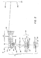
- Illumination optics 11 comprises a light source 29 which is selectable and can be implemented using a number of types of lamp or electro-optical components, as is described subsequently. If light source 29 comprises a halogen lamp, it is advisable to incorporate an infrared rejecting filter 31 following the lamp in the assembly, as shown in Figure 2. Light emitted from light source 29 is focused by a lens 37 and directed to an uniformizer 35.
- Uniformizer 35 comprises two field lenses 36 and 42 and a lenslet array assembly 40, acting as an uniformizer for the light.
- Lenslet array assembly 40 includes two lenslet arrays 40a and 40b.
- Lenses 36 and 37 direct the monochromatic light into the entrance aperture of lenslet array assembly 40.
- Conjugate planes within image forming assembly 10 are indicated by dotted lines 28.
- the light at the intermediate illumination plane is broken into a number of portions equivalent to the number of elements in lenslet array 40a.
- the individual portions are then imaged and magnified by second lenslet array 40b and second field lens 42.
- Light passing through uniformizer 35 along with a following field lens 44 is passed through an optional aperture stop 46 and a relay lens 48.
- Relay lens 48 is positioned immediately before a polarization beamsplitter element 50. It should also be noted that, although relay lens 48 and field lens 44 are shown as separate elements in Figure 2, a single compound lens 49 (not shown) providing uniform illumination could be employed instead of the two individual lens elements 48 and 44 as is depicted in Figure 2.
- linear polarizer 38 may be incorporated prior to polarization beamsplitter element 50. There are several places where a linear polarizer 38 can be placed; one such position is immediately preceding lenslet array assembly 40. Linear polarizer 38 is used to isolate the polarization state parallel to the axis of polarization beamsplitter element 50. This serves to reinforce the polarization state determined by polarization beamsplitter element 50, decrease leakage light and thereby increase the resulting contrast ratio.
- light of the s-polarization state 142 passing through polarization beamsplitter element 50 is directed to the plane of a reflective spatial light modulator 52, which is a reflective LCD in the preferred embodiment.
- the p-polarization state 144 is passed through polarization beamsplitter element 50.
- Field lens 44, relay lens 48, and the polarization beamsplitter element 50 constitute the first lens assembly 41 for directing the polarized light to the spatial light modulator 52.
- spatial light modulator 52 of this system is designed for a two dimensional reflective polarization-based spatial light modulator.
- Spatial light modulator 52 includes a plurality of modulator sites 53, each of which can be individually modulated.
- Light passes through spatial light modulator 52, is reflected off the back reflective surface of spatial light modulator 52, and returns through spatial light modulator 52 to be directed through a second lens assembly 132, which is a print lens assembly, onto an image plane 150 ( Figure 2). If a modulator site 53 is "on" or bright, during the round-trip through spatial light modulator 52, the polarization state of the light is rotated. In an ideal case the light is rotated 90 degrees when modulator site 53 is in an "on" state.
- reflective polarization based modulators are the reflective liquid crystal modulator.
- Such modulators originally developed for use in projection display, can have resolutions as high as 4000 x 2000 modulator sites. Currently, resolutions of 1200 x 1600 sites are available with footprints as small as a 0.9 inch diagonal.
- These high resolution reflective LCDs are often twisted nematic LCDs or homeotropically aligned reflective LCDs, although other types of reflective LCDs such as ferroelectric are often employed in projection display.
- Some of the key characteristics of these LCDs are high resolution, high contrast (>100:1), fast frame rate of 70 frames per second or higher, and high aperture ratios (>90%).
- CMOS backplane increases the uniformity across the array.
- the LCDs are also capable of producing an eight bit gray scale either through pulse width modulation or through analog operation. In either case data is introduced digitally to the printing system, as controlled by control logic processor 210 ( Figure 1). These characteristics ensure that the reflective LCD is an excellent choice for use in a reflective printing system.
- Spatial light modulator 52 can be designed in a number of different configurations. The most amenable to a low cost printing system is a single chip system. In a preferred embodiment, spatial light modulator 52 would be a single-chip device specifically designed for single color use, providing optimum frame speed.
- the light source could have a number of selectable wavelengths. It is thus necessary to use the spatial light modulator 52 with light at a wavelength for which the modulator is not optimized. In such a case, there are methods for obtaining optimum performance. For example, for a given liquid crystal composition, thickness, and applied voltage, the resulting polarization rotation on an incident beam may vary with wavelength so that the efficiency and contrast of the modulation can vary as a function of wavelength. In the bright, or "on" state, this difference in rotation can effect the efficiency of the system. In other words, the percentage of incident light that is actually rotated and imaged on the media plane can vary.
- This difference in wavelength efficiency can be accounted for by adapting the illumination strength and exposure time, based on wavelength, in order to obtain the power density required by the media, using techniques well-known in the imaging art.
- the problem is particularly acute in the dark or "off state". In this state, the light is not rotated and should not be directed through polarization beamsplitter element 50 and imaged. If the light is in fact, rotated, light will leak through the imaging system and decrease the contrast.
- contrast can be adjusted for wavelength using polarization compensation or selection devices.
- a polarization compensator 76 may be introduced to the surface of spatial light modulator 52.
- the top surface or layer includes polarization compensator 76
- the second surface or layer is a cover glass 74 of spatial light modulator 52
- the third layer is spatial light modulator 52 itself, with a reflective backplane.
- Behind spatial light modulator 52 are mounted actuators 70, 72 or mounts for actuators to position spatial light modulator 52.
- An alternate method for contrast adjustment is to incorporate a polarization compensator in the path of the optical beam to correct the polarization state of the light.
- a single compensator may be placed in the optical path to particularly correct the off-state of the light.
- polarization compensation devices can be expensive.
- An efficient but inexpensive means to accomplish the same results can be obtained using linear polarizers.
- a single LCD imparts a degree of polarization rotation dependent on the color of illumination. In an effort to maximize contrast, special care must be taken to provide a truly dark "off state.” Because the rotation of the light from spatial light modulator 52 is not always crossed perfectly with polarization beamsplitter element 50 in the off state, additional polarization selection must be incorporated into the optical path.
- polarization beamsplitter element 50 is not perfect and will leak some amount of light.
- an additional sheet polarizer can be disposed either immediately before or after print lens assembly 132.
- This additional polarizer serves to reject leakage light that is passed through polarization beamsplitter element 50.
- the dark state of the light is actually rotated 7 degrees from the polarization transmitting direction of polarization beamsplitter element 50.
- a second polarizer 134 ( Figure 2) is provided, rotated 7 degrees off-axis to suppress leakage light.
- the particular angle at which polarizer 134 must be placed is a function of the particular reflective LCD chosen for the printing system and the light source selected.
- a suggested placement of polarizer 134 in the optics path is shown in Figure 2.
- dithering may be used to increase the inherent LCD resolution and to compensate for modulator site defects.
- a dithering pattern for a standard high aperture ratio spatial light modulator 52 is shown in Figures 5a-5d.
- spatial light modulator 52 is first positioned at a first modulator position 61 and modulator sites 63 are positioned and imaged ( Figure 5a).
- Spatial light modulator 52 is then moved to a second modulator position 62 ( Figure 5b) which is one half of a modulator site laterally displaced from previous position 61. Spatial light modulator 52 is then imaged at position 62. Spatial light modulator 52 is then displaced one half of a modulator site longitudinally from previous position 62, which means it is diagonally displaced from initial position 61 to a third modulator position 64 ( Figure 5d). Modulator sites 63 are illuminated and the media exposed again. Spatial light modulator 52 is then moved to a fourth modulator position 65 that is laterally displaced from third position 64 ( Figure 5c). The media is then exposed at this position. Using this pattern, there is effectively a fourfold increase in the amount of data written.
- Dithering requires motion of the modulator in two directions. Each increment of motion is approximately between 5 um and 20 um for a typical reflective LCD modulator.
- actuator 54 or motion assemblies as shown in Figure 2, can be employed.
- the assembly can use two piezo-electric actuators.
- the device can be sub-apertured.
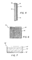
- the modulator can contain an aperture ratio that is relatively small. Ideally this aperture must be symmetrically placed within each modulator site. The result is a modulator site for which only a fraction of the area transmits light. Referring to Figure 6, there is shown an illustration of a sub-apertured area modulator. Black regions 80 represent the non reflecting, non-transmitting regions of the device. Clear areas 82 represent the sub-apertured transmitting areas of the LCD.
- Figure 7 is a cross-sectional view of an alternate two-dimensional LCD spatial light modulator 52'.
- a frame 78' which can be in the form of a CMOS backplane on top of which rests an LCD 76'.
- a cover glass 74' Above the LCD 76' is a cover glass 74'.
- Sub-apertures, to effect the pattern of Figure 6, may exist as a mask in frame 78', as a pattern in LCD 76', or as a pattern on the surface of cover glass 74' closest to LCD 76'.
- a sub-aperture of approximately 25% may be employed. By dithering a 25% aperture ratio device, it is possible to double the resolution in the image.
- Figures 8a-8d represent the dithering of a sub-apertured device.
- Spatial light modulator 52 is positioned at a first modulator position 84 ( Figure 8a) and sub-apertured modulator sites 92 are positioned and exposed while darkened (non reflecting) regions 94 are not imaged onto photosensitive media 160.
- Spatial light modulator 52 is moved to a second modulator position 86 ( Figure 8b) a half full modulator site (sub-aperture and surrounding non-reflective area) laterally displaced from previous position 84. Spatial light modulator 52 is then exposed at position 86.
- Spatial light modulator 52 is then displaced a half a full modulator site longitudinally from previous position 86 to third modulator position 88 ( Figure 8c), which means it is diagonally displaced from the starting point at first modulator position 84. Spatial light modulator 52 is then illuminated and the media exposed again. Spatial light modulator 52 is then moved to a fourth modulator position 90 ( Figure 8d) that is laterally displaced from third position 88. The media is exposed at this position. Effectively, there is a four times increase in the amount of data written. This serves to increase image resolution and to provide means for further image sharpening.
- a sub-aperture of 25% by area, as approximated in Figure 6, will give the highest image quality for a four step dither, however, in an effort to allow for redundancy in the modulator sites, it is better to use a sub-aperture ratio of greater than 25 % by area.
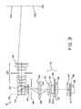
- spatial light modulator 52 is left undithered. But, dithering takes place in one of conjugate image planes 28 as is shown in Figure 9.
- conjugate plane 28 a mask 184 containing the sub-aperture is placed. It is mask 184 that is dithered while the information content to the modulator sites at spatial light modulator 52 is updated. This allows a sub-apertured image to be recorded although the device may not be sub-apertured. It is also possible to create an intermediate image plane, however, this will prove cumbersome.
- mask 184 Another means by which to accomplish the dithering through the use of mask 184 is to place mask 184 in the image plane immediately before photosensitive media 160. This mask 184 can then be dithered while data is refreshed to the device between dither positions. This method of dither will accomplish the same effect as the previous method of the intermediate image.
- Print lens assembly 132 provides the correct demagnification of the image of spatial light modulator 52 to image plane 150 where photosensitive media 160 is located. It should be noted that print lens assembly 132 can be configured for reduction (as is needed for micrographics) or for magnification (as is needed for diagnostic imaging). The configuration of print lens assembly 132 components is dependent on how printer 100 is used. With this arrangement, the same illumination optics 11 and spatial light modulator 52 components can be used with different printer 100 types.
- the optical system designed using the arrangement disclosed in Figure 1 has been shown to be compact, low in cost, and efficient.
- image forming assembly 10 is capable of providing high exposure energy, image forming assembly 10 allows printer 100 to use dry-process media when provided with a light source having sufficient power and wavelength characteristics, thereby providing performance and environmental benefits.
- Printer 100 is capable of achieving sufficient uniformity while retaining the grayscale performance.
- Spatial light modulator 52 alone can receive up to 8 bits of bit depth. However, 8 bits to the modulator may not translate to 8 bits at the media.
- LCD modulators are known to exhibit some measure of roll-off or loss of contrast at the edges of the device.
- the present invention can take advantage of the fact that spatial light modulator 52 designed for projection display generally refresh data faster than is required for printing. Consequently, it is possible to create a single image at the photosensitive media 160 as a super-position of a series of images. The individual images that comprise the final image can vary both in information content and illumination.
- printer 100 can build a composite image out of a series of preliminary images. The superposition of the images of varied information content and varied illumination level introduces additional bit depth to the composite image.
- printer 100 can control image forming assembly 10 to correct for some non-uniformity such as roll-off at spatial light modulator 52 edges.
- One way to accomplish this is to introduce additional image data to spatial light modulator 52, activating only individual modulator sites 53 on the outer edge of spatial light modulator 52. These added images can then be exposed and superimposed on the other images thus giving additional depth to the edge regions.
- An example method would be to scan a series of images taken at LCD spatial light modulator 52, create data maps and convolve all input data with an initial map of LCD spatial light modulator 52 to correct the image. Similar techniques can be used to adjust for modulator non-uniformities that are known prior to operation.
- printer 100 allows a number of alternate embodiments within the scope of the present invention.
- the printing solutions described above provide an adequate bit depth and reasonable timing for use in a COM printer.
- Using the printer of the present invention takes advantage of economical, commodity LCD technology to produce low cost, high resolution prints, with high productivity.
- dithering particularly sub-apertured dithering provides means to further increase the resolution and avoid artifacts due to modulator site failure.
- Light source 29 of illumination optics 11 must provide monochromatic light at a wavelength that is best suited to the sensitivity of photosensitive media 160.
- light source 29 is selectable, allowing printer 100 to utilize any of a number of different types of photosensitive media 160.
- light source 29 comprises one or more LEDs, grouped by emitted wavelength. Referring to Figure 12, there is shown an arrangement of LEDs within a circular aperture 20, for example: red wavelength LEDs 14, green wavelength LEDs 16, and blue wavelength LEDs 18. With this arrangement, the LEDs are distributed so as to provide exposure light evenly. LEDs of a desired color are energized under the control of control logic processor 210, based on the wavelength required for a specific photosensitive media 160.
- printer 100 can be automatically adapted to use one or another type of photosensitive media 160 and to provide the required exposure characteristics needed by that type of photosensitive media 160.
- control logic processor 210 would enable red wavelength LEDs 14, for example.
- FIG. 13 there is shown a cross-sectional view of red LEDs 14, green LEDs 16, and blue LEDs 18 mounted with collimating lenses 32 into a frame 19. Individual collimating lenses 32 are optional but might be useful to aid in encapsulation and position of LEDs 14, 16, and 18.
- a rotatable LED wheel 26 comprises grouped LEDs 14, 16, and 18 that can be rotated into position by control logic processor 210 for providing exposure energy.
- the arrangement of Figure 14 might be most suitable where it is advantageous to obtain concentrated light energy from a close grouping of multiple LEDs 14, 16, and 18.
- the disadvantage presented using the arrangement of Figure 14 relates to rotation of rotatable LED wheel 26, since this requires an added motor or manual operation.
- the preferred embodiment would use distributed LEDs 14, 16, and 18 as shown in Figure 12, arranged for selective energization as electronically switched by control logic processor 210.
- the arrangement of Figure 12 requires no moving parts and can be implemented at lower cost than that shown in Figure 14.
- LEDs 14, 16, and 18 would be specified based on exposure sensitivity characteristics of each type of photosensitive media 160 to be used in printer 100.
- a number of alternate arrangements are possible, including use of LEDs of any suitable color, emitting the desired wavelength.
- different groupings of red LEDs could be used for types of photosensitive media 160 that differ only slightly in terms of wavelength response.
- a single LED could be used for any one photosensitive media 160 type; however, the use of multiple LEDs provides additional output intensity to be directed by image forming assembly 10.
- a halogen lamp 218 could be used to provide a broadband light beam 226 that is transmitted through a selectable filter element 233a, 233b, or 233c contained in a rotatable filter wheel 224 to provide a monochromatic light beam 228.
- Selectable filter elements 233a, 233b, or 233c could be, for example, red, green, and blue filters.
- selectable filter elements 233a, 233b, or 233c could each be red filters, each filter optimized for transmitting a different wavelength in the red visible region.
- monochromatic light beam 228 is output from light source 29 and is directed by image forming assembly 10 to provide exposure energy.
- Control logic processor 210 can include programming logic that provides instructions for which filter 233a, 233b, or 233c to use for a certain photosensitive media 160 type, for example.
- filter 233a, 233b, or 233c could be manually positioned in the optics path by an operator.
- the present invention also allows the use of different types of light sources within the same printer 100. This would enable printer 100, for example, to use red LEDs 14 as light source 29 for one type of media and to use a halogen lamp equipped with a blue filter 33 ( Figure 11) as light source 29 for a different type of media. Different light sources 29 could be moved into or switched into place in the optics path in modular fashion, as needed, based on the media type loaded in printer 100.
- printer 100 can be adapted for monochromatic imaging onto photosensitive media 160 of different types by switching to the appropriate light source 29 using the apparatus and method disclosed herein. It can be appreciated that there could be a number of ways in which selection of a light source 29 could be made by an operator entry or action.
- a sensor 234 connected to control logic processor 210, is disposed to sense an encoding 236 that is coupled to film supply 202.
- Transponder containing a memory that includes identifying data for the media, such as an RF transponder, "SAMPT” ( S elective Addressable M ulti- P age T ransponder), part number “RI-TRP-IR2B” available from Texas Instruments, Incorporated.
- Transceiver such as an RF transceiver, for example, "Model S2000”TM transceiver, available from Texas Instruments, Incorporated, located in Dallas, Texas, USA.
- Magnetically encoded strip Magnetic strip reader Memory device such as an I-button, manufactured by Dallas Semiconductor Corp., Dallas, TX I-button reader Trace pattern, such as an embedded trace pattern Trace pattern reader Encoding 236 could be printed or attached to photosensitive media 160 packaging or could be provided from a network connection or manually entered by an operator. Using this option with the preferred embodiment, upon sensing media 160 type from encoding 236, control logic processor 210 would respond by energizing the appropriate LEDs for the media 160 type.
Landscapes
- Physics & Mathematics (AREA)
- Spectroscopy & Molecular Physics (AREA)
- General Physics & Mathematics (AREA)
- Printers Or Recording Devices Using Electromagnetic And Radiation Means (AREA)
- Projection-Type Copiers In General (AREA)
- Liquid Crystal (AREA)
- Control Of Exposure In Printing And Copying (AREA)
- Microscoopes, Condenser (AREA)
Applications Claiming Priority (2)
| Application Number | Priority Date | Filing Date | Title |
|---|---|---|---|
| US675327 | 2000-09-28 | ||
| US09/675,327 US6480259B1 (en) | 2000-09-28 | 2000-09-28 | Method and apparatus for printing monochromatic images using a spatial light modulator having a selectable light source |
Publications (2)
| Publication Number | Publication Date |
|---|---|
| EP1193542A2 true EP1193542A2 (fr) | 2002-04-03 |
| EP1193542A3 EP1193542A3 (fr) | 2003-07-23 |
Family
ID=24709984
Family Applications (1)
| Application Number | Title | Priority Date | Filing Date |
|---|---|---|---|
| EP01203554A Withdrawn EP1193542A3 (fr) | 2000-09-28 | 2001-09-19 | Méthode et dispositif pour imprimer des images monochromes utilisant un modulateur spatial de lumière avec une source de lumière sélectionnable |
Country Status (3)
| Country | Link |
|---|---|
| US (1) | US6480259B1 (fr) |
| EP (1) | EP1193542A3 (fr) |
| JP (1) | JP2002205426A (fr) |
Cited By (3)
| Publication number | Priority date | Publication date | Assignee | Title |
|---|---|---|---|---|
| GB2400920A (en) * | 2003-04-24 | 2004-10-27 | Eastman Kodak Co | Printing on media of varying contrast |
| WO2010077206A1 (fr) * | 2008-12-31 | 2010-07-08 | Micrographics Data Pte Ltd | Appareil d'archivage de contenu numérique et son procédé |
| IT201800003616A1 (it) * | 2018-03-15 | 2019-09-15 | Polina Bessonova | Sistema di illuminazione per ingranditore fotografico |
Families Citing this family (9)
| Publication number | Priority date | Publication date | Assignee | Title |
|---|---|---|---|---|
| US6580490B1 (en) * | 2000-10-30 | 2003-06-17 | Eastman Kodak Company | Method and apparatus for printing images in multiple formats using a spatial light modulator |
| US6724990B2 (en) * | 2002-08-01 | 2004-04-20 | Eastman Kodak Company | Digital film recorder |
| WO2004104790A2 (fr) | 2003-05-20 | 2004-12-02 | Kagutech Ltd. | Face arriere numerique |
| US7023463B2 (en) * | 2003-07-22 | 2006-04-04 | Eastman Kodak Company | Method and apparatus for printing images from digital image data |
| US6886943B1 (en) * | 2003-10-24 | 2005-05-03 | Jds Uniphase Corporation | High-resolution projection display system |
| JP2006021384A (ja) * | 2004-07-07 | 2006-01-26 | Rohm Co Ltd | 画像形成装置 |
| DE102004038554A1 (de) * | 2004-08-06 | 2006-03-16 | Thomson Broadcast And Media Solutions Gmbh | Filmbelichter und Verfahren zur Belichtung von lichtempfindlichen Filmen |
| US8285131B1 (en) * | 2009-11-18 | 2012-10-09 | Silicon Light Machines Corporation | Apparatus and method for recording an image on photographic film |
| US20110235060A1 (en) * | 2010-03-29 | 2011-09-29 | Hwai-Tzuu Tai | Screened hardcopy reproduction apparatus compensation data calculation |
Citations (8)
| Publication number | Priority date | Publication date | Assignee | Title |
|---|---|---|---|---|
| US4728965A (en) | 1986-06-20 | 1988-03-01 | Eastman Kodak Company | Laser printer having means for correcting laser pointing errors |
| US5325137A (en) | 1991-08-28 | 1994-06-28 | Victor Company Of Japan, Ltd. | Overhead projector with a spatial light modulator |
| US5461411A (en) | 1993-03-29 | 1995-10-24 | Texas Instruments Incorporated | Process and architecture for digital micromirror printer |
| US5504514A (en) | 1992-02-13 | 1996-04-02 | Texas Instruments Incorporated | System and method for solid state illumination for spatial light modulators |
| US5521748A (en) | 1994-06-16 | 1996-05-28 | Eastman Kodak Company | Light modulator with a laser or laser array for exposing image data |
| US5652661A (en) | 1995-06-07 | 1997-07-29 | Eastman Kodak Company | High speed photographic printer using optical and digital printing with an active matrix LCD |
| US5743610A (en) | 1994-12-27 | 1998-04-28 | Seiko Epson Corporation | Projection-type display apparatus |
| US5808800A (en) | 1994-12-22 | 1998-09-15 | Displaytech, Inc. | Optics arrangements including light source arrangements for an active matrix liquid crystal image generator |
Family Cites Families (21)
| Publication number | Priority date | Publication date | Assignee | Title |
|---|---|---|---|---|
| EP0131387B1 (fr) * | 1983-06-15 | 1989-03-08 | Kabushiki Kaisha Toshiba | Capteur d'images à l'état solide à haute résolution |
| US4624558A (en) | 1985-10-15 | 1986-11-25 | Bell & Howell Company | Microimage recorder |
| DE3615780A1 (de) | 1986-05-10 | 1987-11-12 | Agfa Gevaert Ag | Laser computer output mirkofilm-kamera |
| DE3826375A1 (de) | 1988-08-03 | 1990-02-22 | Agfa Gevaert Ag | Computer-output-mikrofilm-printer |
| US5089691A (en) * | 1989-07-11 | 1992-02-18 | Brother Kogyo Kabushiki Kaisha | Image recording apparatus having bar code reader for reading bar code attached to leading end of microcapsule sheet |
| US5015064A (en) * | 1990-04-05 | 1991-05-14 | Photon Imaging Corp. | Electronic printer or scanner using a fiber optic bundle |
| US5049901A (en) * | 1990-07-02 | 1991-09-17 | Creo Products Inc. | Light modulator using large area light sources |
| JPH04171433A (ja) * | 1990-11-02 | 1992-06-18 | Canon Inc | 磁気記憶部付フィルムを用いるカメラ |
| US5315411A (en) * | 1993-01-04 | 1994-05-24 | Eastman Kodak Company | Dithering mechanism for a high resolution imaging system |
| US5745156A (en) | 1994-04-28 | 1998-04-28 | Xerox Corporation | Digital printer using two-dimensional, full frame light valve |
| US5539567A (en) * | 1994-06-16 | 1996-07-23 | Texas Instruments Incorporated | Photolithographic technique and illuminator using real-time addressable phase shift light shift |
| US5701185A (en) | 1994-11-21 | 1997-12-23 | Polaroid Corporation | Spatial light modulator assembly for adapting a photographic printer to print electronic images |
| US5757348A (en) * | 1994-12-22 | 1998-05-26 | Displaytech, Inc. | Active matrix liquid crystal image generator with hybrid writing scheme |
| JP2885155B2 (ja) * | 1995-02-21 | 1999-04-19 | ノーリツ鋼機株式会社 | 写真露光装置 |
| JPH09329846A (ja) * | 1996-06-11 | 1997-12-22 | Fuji Photo Film Co Ltd | 光パターン照射装置及び光パターン照射方法 |
| US5923475A (en) * | 1996-11-27 | 1999-07-13 | Eastman Kodak Company | Laser printer using a fly's eye integrator |
| US6208812B1 (en) * | 1997-05-21 | 2001-03-27 | Fuji Photo Film Co., Ltd. | Camera with bar code reader |
| US5971545A (en) * | 1997-06-25 | 1999-10-26 | Hewlett-Packard Company | Light source for projection display |
| DE19746575A1 (de) * | 1997-10-22 | 1999-04-29 | Zeiss Carl Fa | Optische Bildaufnahmeeinrichtung und Verfahren zu deren Nutzung |
| US6215547B1 (en) * | 1998-11-19 | 2001-04-10 | Eastman Kodak Company | Reflective liquid crystal modulator based printing system |
| US6079833A (en) * | 1999-02-17 | 2000-06-27 | Hughes-Jvc Technology Corporation | Laser imaging using a spatial light modulator |
-
2000
- 2000-09-28 US US09/675,327 patent/US6480259B1/en not_active Expired - Lifetime
-
2001
- 2001-09-19 EP EP01203554A patent/EP1193542A3/fr not_active Withdrawn
- 2001-09-28 JP JP2001301780A patent/JP2002205426A/ja active Pending
Patent Citations (8)
| Publication number | Priority date | Publication date | Assignee | Title |
|---|---|---|---|---|
| US4728965A (en) | 1986-06-20 | 1988-03-01 | Eastman Kodak Company | Laser printer having means for correcting laser pointing errors |
| US5325137A (en) | 1991-08-28 | 1994-06-28 | Victor Company Of Japan, Ltd. | Overhead projector with a spatial light modulator |
| US5504514A (en) | 1992-02-13 | 1996-04-02 | Texas Instruments Incorporated | System and method for solid state illumination for spatial light modulators |
| US5461411A (en) | 1993-03-29 | 1995-10-24 | Texas Instruments Incorporated | Process and architecture for digital micromirror printer |
| US5521748A (en) | 1994-06-16 | 1996-05-28 | Eastman Kodak Company | Light modulator with a laser or laser array for exposing image data |
| US5808800A (en) | 1994-12-22 | 1998-09-15 | Displaytech, Inc. | Optics arrangements including light source arrangements for an active matrix liquid crystal image generator |
| US5743610A (en) | 1994-12-27 | 1998-04-28 | Seiko Epson Corporation | Projection-type display apparatus |
| US5652661A (en) | 1995-06-07 | 1997-07-29 | Eastman Kodak Company | High speed photographic printer using optical and digital printing with an active matrix LCD |
Cited By (3)
| Publication number | Priority date | Publication date | Assignee | Title |
|---|---|---|---|---|
| GB2400920A (en) * | 2003-04-24 | 2004-10-27 | Eastman Kodak Co | Printing on media of varying contrast |
| WO2010077206A1 (fr) * | 2008-12-31 | 2010-07-08 | Micrographics Data Pte Ltd | Appareil d'archivage de contenu numérique et son procédé |
| IT201800003616A1 (it) * | 2018-03-15 | 2019-09-15 | Polina Bessonova | Sistema di illuminazione per ingranditore fotografico |
Also Published As
| Publication number | Publication date |
|---|---|
| JP2002205426A (ja) | 2002-07-23 |
| US6480259B1 (en) | 2002-11-12 |
| EP1193542A3 (fr) | 2003-07-23 |
Similar Documents
| Publication | Publication Date | Title |
|---|---|---|
| US6580490B1 (en) | Method and apparatus for printing images in multiple formats using a spatial light modulator | |
| US6215547B1 (en) | Reflective liquid crystal modulator based printing system | |
| EP1174752B1 (fr) | Procédé et dispositif pour imprimer sur un support photosensible utilisant plusieurs modulateurs spatiaux de lumière | |
| EP1177908B1 (fr) | Méthode et appareil d'impression monochrome en utilisant un modulateur spatial de lumière | |
| EP1291711B1 (fr) | Imprimante pour matériau photosensible comprenant une source lumineuse hybride | |
| EP1285769B1 (fr) | Procédé et appareil pour l'impression d'images à haute résolution en utilisant des modulateurs spatiaux de lumière à réflexions multiples | |
| US6646716B1 (en) | Method and apparatus for printing multiple simultaneous images onto a photosensitive media | |
| US6624949B2 (en) | Printing apparatus for photosensitive media using dichroic prism in illumination path | |
| US6480259B1 (en) | Method and apparatus for printing monochromatic images using a spatial light modulator having a selectable light source | |
| US6930797B2 (en) | Method and apparatus for printing high resolution images using multiple reflective spatial light modulators | |
| US6330018B1 (en) | Method and apparatus for printing high resolution images using reflective LCD modulators | |
| US6980280B2 (en) | Two level image writer | |
| US5982407A (en) | Color printer | |
| US7023463B2 (en) | Method and apparatus for printing images from digital image data | |
| US6734889B2 (en) | Color printer comprising a linear grating spatial light modulator | |
| US7164434B2 (en) | LCD based imaging apparatus for printing multiple formats | |
| US20070153080A1 (en) | High-speed continuous film writer |
Legal Events
| Date | Code | Title | Description |
|---|---|---|---|
| PUAI | Public reference made under article 153(3) epc to a published international application that has entered the european phase |
Free format text: ORIGINAL CODE: 0009012 |
|
| AK | Designated contracting states |
Kind code of ref document: A2 Designated state(s): AT BE CH CY DE DK ES FI FR GB GR IE IT LI LU MC NL PT SE TR |
|
| AX | Request for extension of the european patent |
Free format text: AL;LT;LV;MK;RO;SI |
|
| PUAL | Search report despatched |
Free format text: ORIGINAL CODE: 0009013 |
|
| AK | Designated contracting states |
Designated state(s): AT BE CH CY DE DK ES FI FR GB GR IE IT LI LU MC NL PT SE TR |
|
| AX | Request for extension of the european patent |
Extension state: AL LT LV MK RO SI |
|
| RIC1 | Information provided on ipc code assigned before grant |
Ipc: 7B 41J 2/447 B Ipc: 7G 03B 27/72 A |
|
| 17P | Request for examination filed |
Effective date: 20031219 |
|
| AKX | Designation fees paid |
Designated state(s): DE FR GB |
|
| 17Q | First examination report despatched |
Effective date: 20041213 |
|
| STAA | Information on the status of an ep patent application or granted ep patent |
Free format text: STATUS: THE APPLICATION IS DEEMED TO BE WITHDRAWN |
|
| 18D | Application deemed to be withdrawn |
Effective date: 20050728 |