EP1197801A1 - Lithographisches Gerät mit zwei Objekthaltern - Google Patents
Lithographisches Gerät mit zwei Objekthaltern Download PDFInfo
- Publication number
- EP1197801A1 EP1197801A1 EP01126286A EP01126286A EP1197801A1 EP 1197801 A1 EP1197801 A1 EP 1197801A1 EP 01126286 A EP01126286 A EP 01126286A EP 01126286 A EP01126286 A EP 01126286A EP 1197801 A1 EP1197801 A1 EP 1197801A1
- Authority
- EP
- European Patent Office
- Prior art keywords
- unit
- displacement
- relative
- parallel
- positioning device
- Prior art date
- Legal status (The legal status is an assumption and is not a legal conclusion. Google has not performed a legal analysis and makes no representation as to the accuracy of the status listed.)
- Granted
Links
Images




Classifications
-
- G—PHYSICS
- G03—PHOTOGRAPHY; CINEMATOGRAPHY; ANALOGOUS TECHNIQUES USING WAVES OTHER THAN OPTICAL WAVES; ELECTROGRAPHY; HOLOGRAPHY
- G03F—PHOTOMECHANICAL PRODUCTION OF TEXTURED OR PATTERNED SURFACES, e.g. FOR PRINTING, FOR PROCESSING OF SEMICONDUCTOR DEVICES; MATERIALS THEREFOR; ORIGINALS THEREFOR; APPARATUS SPECIALLY ADAPTED THEREFOR
- G03F7/00—Photomechanical, e.g. photolithographic, production of textured or patterned surfaces, e.g. printing surfaces; Materials therefor, e.g. comprising photoresists; Apparatus specially adapted therefor
- G03F7/70—Microphotolithographic exposure; Apparatus therefor
- G03F7/70691—Handling of masks or workpieces
- G03F7/70733—Handling masks and workpieces, e.g. exchange of workpiece or mask, transport of workpiece or mask
-
- G—PHYSICS
- G03—PHOTOGRAPHY; CINEMATOGRAPHY; ANALOGOUS TECHNIQUES USING WAVES OTHER THAN OPTICAL WAVES; ELECTROGRAPHY; HOLOGRAPHY
- G03F—PHOTOMECHANICAL PRODUCTION OF TEXTURED OR PATTERNED SURFACES, e.g. FOR PRINTING, FOR PROCESSING OF SEMICONDUCTOR DEVICES; MATERIALS THEREFOR; ORIGINALS THEREFOR; APPARATUS SPECIALLY ADAPTED THEREFOR
- G03F7/00—Photomechanical, e.g. photolithographic, production of textured or patterned surfaces, e.g. printing surfaces; Materials therefor, e.g. comprising photoresists; Apparatus specially adapted therefor
- G03F7/70—Microphotolithographic exposure; Apparatus therefor
- G03F7/70691—Handling of masks or workpieces
- G03F7/70775—Position control, e.g. interferometers or encoders for determining the stage position
-
- B—PERFORMING OPERATIONS; TRANSPORTING
- B23—MACHINE TOOLS; METAL-WORKING NOT OTHERWISE PROVIDED FOR
- B23Q—DETAILS, COMPONENTS, OR ACCESSORIES FOR MACHINE TOOLS, e.g. ARRANGEMENTS FOR COPYING OR CONTROLLING; MACHINE TOOLS IN GENERAL CHARACTERISED BY THE CONSTRUCTION OF PARTICULAR DETAILS OR COMPONENTS; COMBINATIONS OR ASSOCIATIONS OF METAL-WORKING MACHINES, NOT DIRECTED TO A PARTICULAR RESULT
- B23Q1/00—Members which are comprised in the general build-up of a form of machine, particularly relatively large fixed members
- B23Q1/25—Movable or adjustable work or tool supports
- B23Q1/44—Movable or adjustable work or tool supports using particular mechanisms
- B23Q1/56—Movable or adjustable work or tool supports using particular mechanisms with sliding pairs only, the sliding pairs being the first two elements of the mechanism
- B23Q1/60—Movable or adjustable work or tool supports using particular mechanisms with sliding pairs only, the sliding pairs being the first two elements of the mechanism two sliding pairs only, the sliding pairs being the first two elements of the mechanism
- B23Q1/62—Movable or adjustable work or tool supports using particular mechanisms with sliding pairs only, the sliding pairs being the first two elements of the mechanism two sliding pairs only, the sliding pairs being the first two elements of the mechanism with perpendicular axes, e.g. cross-slides
- B23Q1/621—Movable or adjustable work or tool supports using particular mechanisms with sliding pairs only, the sliding pairs being the first two elements of the mechanism two sliding pairs only, the sliding pairs being the first two elements of the mechanism with perpendicular axes, e.g. cross-slides a single sliding pair followed perpendicularly by a single sliding pair
-
- B—PERFORMING OPERATIONS; TRANSPORTING
- B23—MACHINE TOOLS; METAL-WORKING NOT OTHERWISE PROVIDED FOR
- B23Q—DETAILS, COMPONENTS, OR ACCESSORIES FOR MACHINE TOOLS, e.g. ARRANGEMENTS FOR COPYING OR CONTROLLING; MACHINE TOOLS IN GENERAL CHARACTERISED BY THE CONSTRUCTION OF PARTICULAR DETAILS OR COMPONENTS; COMBINATIONS OR ASSOCIATIONS OF METAL-WORKING MACHINES, NOT DIRECTED TO A PARTICULAR RESULT
- B23Q1/00—Members which are comprised in the general build-up of a form of machine, particularly relatively large fixed members
- B23Q1/25—Movable or adjustable work or tool supports
- B23Q1/44—Movable or adjustable work or tool supports using particular mechanisms
- B23Q1/56—Movable or adjustable work or tool supports using particular mechanisms with sliding pairs only, the sliding pairs being the first two elements of the mechanism
- B23Q1/60—Movable or adjustable work or tool supports using particular mechanisms with sliding pairs only, the sliding pairs being the first two elements of the mechanism two sliding pairs only, the sliding pairs being the first two elements of the mechanism
- B23Q1/62—Movable or adjustable work or tool supports using particular mechanisms with sliding pairs only, the sliding pairs being the first two elements of the mechanism two sliding pairs only, the sliding pairs being the first two elements of the mechanism with perpendicular axes, e.g. cross-slides
- B23Q1/621—Movable or adjustable work or tool supports using particular mechanisms with sliding pairs only, the sliding pairs being the first two elements of the mechanism two sliding pairs only, the sliding pairs being the first two elements of the mechanism with perpendicular axes, e.g. cross-slides a single sliding pair followed perpendicularly by a single sliding pair
- B23Q1/623—Movable or adjustable work or tool supports using particular mechanisms with sliding pairs only, the sliding pairs being the first two elements of the mechanism two sliding pairs only, the sliding pairs being the first two elements of the mechanism with perpendicular axes, e.g. cross-slides a single sliding pair followed perpendicularly by a single sliding pair followed perpendicularly by a single rotating pair
-
- B—PERFORMING OPERATIONS; TRANSPORTING
- B23—MACHINE TOOLS; METAL-WORKING NOT OTHERWISE PROVIDED FOR
- B23Q—DETAILS, COMPONENTS, OR ACCESSORIES FOR MACHINE TOOLS, e.g. ARRANGEMENTS FOR COPYING OR CONTROLLING; MACHINE TOOLS IN GENERAL CHARACTERISED BY THE CONSTRUCTION OF PARTICULAR DETAILS OR COMPONENTS; COMBINATIONS OR ASSOCIATIONS OF METAL-WORKING MACHINES, NOT DIRECTED TO A PARTICULAR RESULT
- B23Q11/00—Accessories fitted to machine tools for keeping tools or parts of the machine in good working condition or for cooling work; Safety devices specially combined with or arranged in, or specially adapted for use in connection with, machine tools
- B23Q11/0032—Arrangements for preventing or isolating vibrations in parts of the machine
-
- G—PHYSICS
- G03—PHOTOGRAPHY; CINEMATOGRAPHY; ANALOGOUS TECHNIQUES USING WAVES OTHER THAN OPTICAL WAVES; ELECTROGRAPHY; HOLOGRAPHY
- G03F—PHOTOMECHANICAL PRODUCTION OF TEXTURED OR PATTERNED SURFACES, e.g. FOR PRINTING, FOR PROCESSING OF SEMICONDUCTOR DEVICES; MATERIALS THEREFOR; ORIGINALS THEREFOR; APPARATUS SPECIALLY ADAPTED THEREFOR
- G03F7/00—Photomechanical, e.g. photolithographic, production of textured or patterned surfaces, e.g. printing surfaces; Materials therefor, e.g. comprising photoresists; Apparatus specially adapted therefor
- G03F7/70—Microphotolithographic exposure; Apparatus therefor
- G03F7/70691—Handling of masks or workpieces
- G03F7/70716—Stages
-
- G—PHYSICS
- G03—PHOTOGRAPHY; CINEMATOGRAPHY; ANALOGOUS TECHNIQUES USING WAVES OTHER THAN OPTICAL WAVES; ELECTROGRAPHY; HOLOGRAPHY
- G03F—PHOTOMECHANICAL PRODUCTION OF TEXTURED OR PATTERNED SURFACES, e.g. FOR PRINTING, FOR PROCESSING OF SEMICONDUCTOR DEVICES; MATERIALS THEREFOR; ORIGINALS THEREFOR; APPARATUS SPECIALLY ADAPTED THEREFOR
- G03F7/00—Photomechanical, e.g. photolithographic, production of textured or patterned surfaces, e.g. printing surfaces; Materials therefor, e.g. comprising photoresists; Apparatus specially adapted therefor
- G03F7/70—Microphotolithographic exposure; Apparatus therefor
- G03F7/70691—Handling of masks or workpieces
- G03F7/70733—Handling masks and workpieces, e.g. exchange of workpiece or mask, transport of workpiece or mask
- G03F7/70741—Handling masks outside exposure position, e.g. reticle libraries
-
- G—PHYSICS
- G03—PHOTOGRAPHY; CINEMATOGRAPHY; ANALOGOUS TECHNIQUES USING WAVES OTHER THAN OPTICAL WAVES; ELECTROGRAPHY; HOLOGRAPHY
- G03F—PHOTOMECHANICAL PRODUCTION OF TEXTURED OR PATTERNED SURFACES, e.g. FOR PRINTING, FOR PROCESSING OF SEMICONDUCTOR DEVICES; MATERIALS THEREFOR; ORIGINALS THEREFOR; APPARATUS SPECIALLY ADAPTED THEREFOR
- G03F7/00—Photomechanical, e.g. photolithographic, production of textured or patterned surfaces, e.g. printing surfaces; Materials therefor, e.g. comprising photoresists; Apparatus specially adapted therefor
- G03F7/70—Microphotolithographic exposure; Apparatus therefor
- G03F7/70691—Handling of masks or workpieces
- G03F7/70733—Handling masks and workpieces, e.g. exchange of workpiece or mask, transport of workpiece or mask
- G03F7/7075—Handling workpieces outside exposure position, e.g. SMIF box
-
- G—PHYSICS
- G03—PHOTOGRAPHY; CINEMATOGRAPHY; ANALOGOUS TECHNIQUES USING WAVES OTHER THAN OPTICAL WAVES; ELECTROGRAPHY; HOLOGRAPHY
- G03F—PHOTOMECHANICAL PRODUCTION OF TEXTURED OR PATTERNED SURFACES, e.g. FOR PRINTING, FOR PROCESSING OF SEMICONDUCTOR DEVICES; MATERIALS THEREFOR; ORIGINALS THEREFOR; APPARATUS SPECIALLY ADAPTED THEREFOR
- G03F7/00—Photomechanical, e.g. photolithographic, production of textured or patterned surfaces, e.g. printing surfaces; Materials therefor, e.g. comprising photoresists; Apparatus specially adapted therefor
- G03F7/70—Microphotolithographic exposure; Apparatus therefor
- G03F7/70691—Handling of masks or workpieces
- G03F7/70766—Reaction force control means, e.g. countermass
-
- G—PHYSICS
- G03—PHOTOGRAPHY; CINEMATOGRAPHY; ANALOGOUS TECHNIQUES USING WAVES OTHER THAN OPTICAL WAVES; ELECTROGRAPHY; HOLOGRAPHY
- G03F—PHOTOMECHANICAL PRODUCTION OF TEXTURED OR PATTERNED SURFACES, e.g. FOR PRINTING, FOR PROCESSING OF SEMICONDUCTOR DEVICES; MATERIALS THEREFOR; ORIGINALS THEREFOR; APPARATUS SPECIALLY ADAPTED THEREFOR
- G03F7/00—Photomechanical, e.g. photolithographic, production of textured or patterned surfaces, e.g. printing surfaces; Materials therefor, e.g. comprising photoresists; Apparatus specially adapted therefor
- G03F7/70—Microphotolithographic exposure; Apparatus therefor
- G03F7/708—Construction of apparatus, e.g. environment aspects, hygiene aspects or materials
- G03F7/70858—Environment aspects, e.g. pressure of beam-path gas, temperature
- G03F7/709—Vibration, e.g. vibration detection, compensation, suppression or isolation
-
- G—PHYSICS
- G03—PHOTOGRAPHY; CINEMATOGRAPHY; ANALOGOUS TECHNIQUES USING WAVES OTHER THAN OPTICAL WAVES; ELECTROGRAPHY; HOLOGRAPHY
- G03F—PHOTOMECHANICAL PRODUCTION OF TEXTURED OR PATTERNED SURFACES, e.g. FOR PRINTING, FOR PROCESSING OF SEMICONDUCTOR DEVICES; MATERIALS THEREFOR; ORIGINALS THEREFOR; APPARATUS SPECIALLY ADAPTED THEREFOR
- G03F7/00—Photomechanical, e.g. photolithographic, production of textured or patterned surfaces, e.g. printing surfaces; Materials therefor, e.g. comprising photoresists; Apparatus specially adapted therefor
- G03F7/70—Microphotolithographic exposure; Apparatus therefor
- G03F7/708—Construction of apparatus, e.g. environment aspects, hygiene aspects or materials
- G03F7/70991—Connection with other apparatus, e.g. multiple exposure stations, particular arrangement of exposure apparatus and pre-exposure and/or post-exposure apparatus; Shared apparatus, e.g. having shared radiation source, shared mask or workpiece stage, shared base-plate; Utilities, e.g. cable, pipe or wireless arrangements for data, power, fluids or vacuum
-
- G—PHYSICS
- G03—PHOTOGRAPHY; CINEMATOGRAPHY; ANALOGOUS TECHNIQUES USING WAVES OTHER THAN OPTICAL WAVES; ELECTROGRAPHY; HOLOGRAPHY
- G03F—PHOTOMECHANICAL PRODUCTION OF TEXTURED OR PATTERNED SURFACES, e.g. FOR PRINTING, FOR PROCESSING OF SEMICONDUCTOR DEVICES; MATERIALS THEREFOR; ORIGINALS THEREFOR; APPARATUS SPECIALLY ADAPTED THEREFOR
- G03F9/00—Registration or positioning of originals, masks, frames, photographic sheets or textured or patterned surfaces, e.g. automatically
- G03F9/70—Registration or positioning of originals, masks, frames, photographic sheets or textured or patterned surfaces, e.g. automatically for microlithography
- G03F9/7003—Alignment type or strategy, e.g. leveling, global alignment
- G03F9/7023—Aligning or positioning in direction perpendicular to substrate surface
-
- G—PHYSICS
- G03—PHOTOGRAPHY; CINEMATOGRAPHY; ANALOGOUS TECHNIQUES USING WAVES OTHER THAN OPTICAL WAVES; ELECTROGRAPHY; HOLOGRAPHY
- G03F—PHOTOMECHANICAL PRODUCTION OF TEXTURED OR PATTERNED SURFACES, e.g. FOR PRINTING, FOR PROCESSING OF SEMICONDUCTOR DEVICES; MATERIALS THEREFOR; ORIGINALS THEREFOR; APPARATUS SPECIALLY ADAPTED THEREFOR
- G03F9/00—Registration or positioning of originals, masks, frames, photographic sheets or textured or patterned surfaces, e.g. automatically
- G03F9/70—Registration or positioning of originals, masks, frames, photographic sheets or textured or patterned surfaces, e.g. automatically for microlithography
- G03F9/7073—Alignment marks and their environment
- G03F9/7084—Position of mark on substrate, i.e. position in (x, y, z) of mark, e.g. buried or resist covered mark, mark on rearside, at the substrate edge, in the circuit area, latent image mark, marks in plural levels
-
- H—ELECTRICITY
- H10—SEMICONDUCTOR DEVICES; ELECTRIC SOLID-STATE DEVICES NOT OTHERWISE PROVIDED FOR
- H10P—GENERIC PROCESSES OR APPARATUS FOR THE MANUFACTURE OR TREATMENT OF DEVICES COVERED BY CLASS H10
- H10P72/00—Handling or holding of wafers, substrates or devices during manufacture or treatment thereof
- H10P72/50—Handling or holding of wafers, substrates or devices during manufacture or treatment thereof for positioning, orientation or alignment
- H10P72/57—Mask-wafer alignment
-
- Y—GENERAL TAGGING OF NEW TECHNOLOGICAL DEVELOPMENTS; GENERAL TAGGING OF CROSS-SECTIONAL TECHNOLOGIES SPANNING OVER SEVERAL SECTIONS OF THE IPC; TECHNICAL SUBJECTS COVERED BY FORMER USPC CROSS-REFERENCE ART COLLECTIONS [XRACs] AND DIGESTS
- Y10—TECHNICAL SUBJECTS COVERED BY FORMER USPC
- Y10T—TECHNICAL SUBJECTS COVERED BY FORMER US CLASSIFICATION
- Y10T74/00—Machine element or mechanism
- Y10T74/20—Control lever and linkage systems
- Y10T74/20207—Multiple controlling elements for single controlled element
- Y10T74/20213—Interconnected
Definitions
- the present invention relates to lithographic devices for imaging a mask pattern onto a substrate.
- a positioning device of the kind mentioned in the opening paragraph is known from EP-A-0 525 872.
- the known positioning device is used in an optical lithographic device for the manufacture of integrated semiconductor circuits by means of an optical lithographic process.
- the lithographic device images sub-patterns of such semiconductor circuits present on a mask on a reduced scale on a semiconductor substrate by means of a light source and a system of lenses. Since such semiconductor circuits have a complicated structure, the semiconductor substrates should be exposed a number of times, each time with a different mask having a different sub-pattem.
- the masks are consecutively taken from a magazine and placed in an operational position in the lithographic device by means of the known positioning device.
- the mask During the displacement of a mask from the magazine to the operational position, the mask passes a measuring position where a position is measured occupied by the mask relative to a reference of the lithographic device.
- a position of the object holder by means of which the mask is displaced is measured relative to said reference during the displacement of the mask from the measuring position into the operational position, so that the mask can be placed in a desired operational position with respect to the reference through a suitable displacement of the object holder.
- the relevant object holder keeps the mask in the desired operational position during the exposure of the semiconductor substrate. Meanwhile, the other object holder takes a next mask from the magazine and moves it into the measuring position.
- the use of the two displacement units with the two object holders thus renders it possible to measure the position of a subsequent mask relative to the reference already while a previous mask is in the operational position and the semiconductor substrate is being exposed through this previous mask.
- the manufacturing output of the lithographic device is considerably increased in this manner.
- a positioning device of the kind mentioned in the opening paragraph is generally known in machine tools and machining installations.
- a position occupied by a workpiece supported by one of the two object holders relative to this object holder is measured in the measuring position.
- the relevant object holder with the workpiece is moved into the operational position in which the workpiece is to be machined.
- a position occupied by the relevant object holder relative to a reference of the machine tool is measured in the operational position, with the result that the workpiece can be brought into a desired operational position with respect to the reference.
- the use of the two displacement units with the two object tables considerably increases the manufacturing output of the machine tools or machining installation because a next workpiece is already moved into the measuring position while a former workpiece is being processed.
- the first and the second displacement unit of the known positioning device each comprise a first part which is fastened to the relevant object holder and a second part which is fastened to the base, said first part and second part of each displacement unit being displaceable relative to one another while exerting a driving force on one another.
- a disadvantage of the known positioning device is that the two parts of the displacement units are each fastened to the base, which accordingly forms a common base for the first and the second displacement unit. Reaction forces are exerted on the second parts during the displacement of the object holders, which forces are transmitted into the base. Said reaction forces lead to mechanical vibrations in the base, which in their turn are transmitted to the second parts and to the object holders.
- the first object holder If the first object holder is present, for example, in the operational position, mechanical vibrations will arise in the first object holder as a result of the reaction forces exerted on the base by the second displacement unit during the displacement of a next mask from the magazine to the measuring position. Such a mutual interference between the two displacement units leads to positioning inaccuracies of the displacement units, which are usually undesirable. In addition, the mechanical vibrations generated in the base are also transmitted to the other parts of the device in which the known positioning device is used, which is usually also undesirable.
- a lithographic device comprising:
- force actuator is understood to mean an actuator for generating a driving force with a predetermined value.
- position actuators are known for generating displacements having a predetermined value.
- a special embodiment of a positioning device is characterized in that the balancing unit comprises a support body which is provided with a guiding surface which extends parallel to the X-direction and parallel to the Y-direction, which is common to the two object holders, and along which the two object holders are displaceable parallel to the X-direction and parallel to the Y-direction, said object holders being both provided with a coupling member by means of which the relevant object holder can be coupled in turn to the first part of the X-actuator of the first displacement unit and to the first part of the X-actuator of the second displacement unit.
- the object holders in this embodiment are displaceably guided over the common guiding surface belonging to the balancing unit, for example by means of static gas bearings.
- the support body is, for example, a granite slab and has a dual function, i.e. supporting and guiding the two object holders, and forming a balancing unit for the two displacement units.
- the object holders When the first object holder is being moved from the measuring position into the operational position and the second object holder is being moved from the operational position into the measuring position, the object holders must pass one another over the common guiding surface. To achieve this, the first object holder is displaced from the measuring position into a first intermediate position between the measuring position and the operational position by means of the first displacement unit, while the second object holder is displaced from the operational position into a second intermediate position next to the first intermediate position between the measuring position and the operational position by means of the second displacement unit.
- the first object holder is uncoupled from the first displacement unit and coupled to the second displacement unit, whereas the second object holder is uncoupled from the second displacement unit and coupled to the first displacement unit. Then the first object holder is moved from the first intermediate position into the operational position by the second displacement unit, while the second object holder is moved from the second intermediate position into the measuring position by the first displacement unit. Since the object holders are provided with said coupling members, a distance over which the first parts of the displacement units must be displaceable relative to the relevant cooperating second parts of the displacement units is reduced, so that the required dimensions of the displacement units are reduced. It is in addition prevented that the displaceable parts of the first displacement unit and the displaceable parts of the second displacement unit must be capable of passing one another, which would lead to a comparatively complicated construction of the displacement units.
- a further embodiment of a positioning device is characterized in that the coupling members of the object holders each comprise an XY Lorentz force actuator which is provided with a first part fastened to the relevant object holder and with a second part fastened to the first part of the X-actuator of the relevant displacement unit, the first parts of the XY Lorentz force actuators each being capable of cooperation with the second parts of the two XY Lorentz force actuators.
- Said XY Lorentz force actuators each have a dual function, so that a simple and practical construction of the positioning device is provided.
- the object holders can each be displaced over comparatively small distances and with comparatively high accuracies relative to the first part of the X-actuator of the relevant displacement unit by means of said XY Lorentz force actuators. Since the first part and the second part of such a Lorentz force actuator are coupled to one another exclusively by means of a Lorentz force, said parts can be mutually uncoupled and coupled in a simple manner through deactivation and activation, respectively, of the Lorentz force.
- a construction of the first parts of the XY Lorentz force actuators such that they can each cooperate with both second parts of the XY Lorentz force actuators has the result that the first part of each of the two XY Lorentz force actuators can be taken over by the second part of the other XY Lorentz force actuator in said intermediate positions of the object holders.
- the invention also provides a method of manufacturing a semiconductor device using a lithographic device, the method comprising the steps of:
- the lithographic device according to the invention shown diagrammatically in Fig. 1 is used for the manufacture of integrated semiconductor circuits by an optical lithographic process and by means of an imaging method which follows the so-called "step and repeat" principle.
- the lithographic device is provided with a frame 1 which supports in that order, as seen parallel to a vertical Z-direction, a positioning device 3 according to the invention, a focusing unit 5, a mask holder 7, and a radiation source 9.
- the positioning device 3 comprises a first substrate holder 11 and an identical second substrate holder 13.
- the lithographic device shown in Fig. 1 is an optical lithographic device whose radiation source 9 comprises a light source 15.
- the substrate holders 11 and 13 comprise a support surface 17 which extends perpendicularly to the Z-direction and on which a first semiconductor substrate 19 can be placed and a support surface 21 which extends perpendicularly to the Z-direction and on which a second semiconductor substrate 23 can be placed, respectively.
- the first substrate holder 11 is displaceable relative to the frame 1 parallel to an X-direction perpendicular to the Z-direction and parallel to a Y-direction perpendicular to the X-direction and perpendicular to the Z-direction by means of a first displacement unit 25 of the positioning device 3, while the second substrate holder 13 is displaceable relative to the frame 1 parallel to the X-direction and parallel to the Y-direction by means of a second displacement unit 27 of the positioning device 3.
- the focusing unit 5 is an imaging or projection system and comprises an optical lens system 29 with an optical main axis 31 directed parallel to the Z-direction and an optical reduction factor which is, for example, 4 or 5.
- the mask holder 7 comprises a support surface 33 which extends perpendicularly to the Z-direction and on which a mask 35 can be placed.
- the mask 35 comprises a pattern or a sub-pattern of an integrated semiconductor circuit.
- a light beam originating from the light source 15 is guided through the mask 35 and focused on the first semiconductor substrate 19 by means of the lens system 29, so that the pattern present on the mask 35 is imaged on a reduced scale on the first semiconductor substrate 19.
- the first semiconductor substrate 19 comprises a large number of individual fields on which identical semiconductor circuits are provided. The fields of the first semiconductor substrate 19 are consecutively exposed through the mask 35 for this purpose.
- the first semiconductor substrate 19 and the mask 35 are in fixed positions relative to the focusing unit 5, whereas after the exposure of an individual field a next field is brought into position relative to the focusing unit 5 each time in that the first substrate holder 11 is displaced parallel to the X-direction and/or parallel to the Y-direction by the first displacement unit 25.
- This process is repeated a number of times, with a different mask each time, so that complicated integrated semiconductor circuits with a layered structure are manufactured.
- the integrated semiconductor circuits to be manufactured by means of the lithographic device have a structure with detail dimensions which lie in the sub-micron range.
- the semiconductor substrate 19 Since the first semiconductor substrate 19 is exposed consecutively through a number of different masks, the pattern present on these masks should be imaged on the semiconductor substrate 19 with an accuracy which also lies in the sub-micron range, or even in the nanometer range. Therefore, the semiconductor substrate 19 must be positioned relative to the focusing unit 5 with a comparable accuracy between two consecutive exposure steps, so that very high requirements are imposed on the positioning accuracy of the positioning device 3.
- a batch of semiconductor substrates under manufacture is consecutively exposed through the mask 35 in the lithographic device shown in Fig. 1, whereupon said batch is consecutively exposed through a next mask. This process is repeated a number of times, each time with another mask.
- the semiconductor substrates to be exposed are present in a magazine from which the semiconductor substrates are transported consecutively into a measuring position of the positioning device 3 by means of a transport mechanism. Said magazine and said transport mechanism, which are both of a kind usual and known per se, are not shown in Fig. 1 for simplicity's sake.
- the first substrate holder 11 is in an operational position in which the first semiconductor substrate 19 placed on the first substrate holder 11 can be irradiated by the radiation source 9 through the focusing unit 5.
- the second substrate holder 13 is in said measuring position of the positioning device 3, in which a position of the second semiconductor substrate 23 placed on the second substrate holder 13 relative to the second substrate holder 13 can be measured in directions parallel to the X-direction and parallel to the Y-direction by means of an optical position measuring unit 37 of the lithographic device, which unit is depicted diagrammatically only in Fig. 1, and in which the second semiconductor substrate 23 is positioned with respect to the second substrate holder 13 with a predetermined accuracy by means of said transport mechanism.
- the optical position measuring unit 37 is also fastened to the frame 1.
- the first substrate holder 11 is displaced by the positioning device 3 in a manner to be further explained below from the operational position into the measuring position, from whence the first semiconductor substrate 19 is returned to the magazine by said transport mechanism.
- the second semiconductor substrate 23 is displaced from the measuring position into the operational position by the positioning device 3 in a manner to be further explained below.
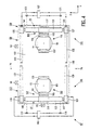
- Figs. 2 and 3 show a first embodiment of a positioning device 3 according to the invention which is suitable for use in the lithographic device of Fig. 1.
- the two displacement units 25 and 27 of the positioning device 3 are each provided with an X-actuator 39, 41 and a Y-actuator 43, 45.
- the X-actuators 39, 41 are each provided with a first part 47, 49 which extends parallel to the X-direction, which is fastened to the substrate holder 11, 13 of the relevant displacement unit 25, 27, and which is displaceable relative to a second part 51, 53 of the relevant X-actuator 39, 41.
- the Y-actuators 43, 45 are each provided with a first part 55, 57 which is fastened to the second part 51, 53 of the X-actuator 39, 41 of the relevant displacement unit 25, 27 and which is displaceable relative to a second part 59, 61 of the relevant Y-actuator 43, 45 which extends parallel to the Y-direction.
- the X-actuators 39, 41 and the Y-actuators 43, 45 are so-called force actuators, wherein the first parts 47, 49 and the cooperating second parts 51, 53 of the X-actuators 39, 41 exert a mutual driving force of a predetermined value parallel to the X-direction during operation, while the first parts 55, 57 and the cooperating second parts 59, 61 of the Y-actuators 43, 45 exert a mutual driving force parallel to the Y-direction during operation which also has a predetermined value.
- the force actuators are, for example, so-called linear Lorentz force motors which are usual and known per se and which generate exclusively a Lorentz force of a predetermined value during operation.
- the substrate holders 11, 13 are thus each displaceable parallel to the X-direction independently of one another by means of a suitable driving force of the X-actuator 43, 45 of the relevant displacement unit 25, 27.
- the substrate holders 11, 13, each together with the X-actuator 43, 45 of the relevant displacement unit 25, 27, are displaceable parallel to the Y-direction independently of one another by means of a suitable driving force of the Y-actuator 43, 45 of the relevant displacement unit 25, 27.
- the Y-actuators 43, 45 of the displacement units 25, 27 are provided with a common straight guide 63 along which the first parts 55 and 57 of the Y-actuators 43 and 45 are displaceably guided, seen parallel to the Y-direction.
- the positioning device 3 is further provided with a rotatable unit 65 which is shown diagrammatically only in the Figures and which is provided with a first disc-shaped part 67 which is fastened to a balancing unit 69 of the positioning device 3 to be described in more detail below, and a second disc-shaped part 71 which is fastened to the common straight guide 63.
- the second disc-shaped part 71 is rotatable relative to the first disc-shaped part 67 about an axis of rotation 73 which extends parallel to the Z-direction.
- the rotatable unit 65 is provided with an electric motor 75 which is depicted diagrammatically only in the Figures and which is fastened to the balancing unit 69 and coupled to the second disc-shaped part 71 by means of a drive belt 77.
- the second disc-shaped part 71 of the rotatable unit 65 is rotatated about the axis of rotation 73 through an angle of 180° relative to the first disc-shaped part 67, so that the common straight guide 63 together with the first displacement unit 25 and the second displacement unit 27 is rotated about the axis of rotation 73.
- Said rotation of the common straight guide 63 causes the first displacement unit 25 with the first substrate holder 11 to be displaced in its entirety from the operational position into the measuring position, while the second displacement unit 27 with the second substrate holder 13 is displaced in its entirety from the measuring position into the operational position.
- Fig. 3 shows the positioning device 3 in a position in which the common straight guide 63 has performed part of the total rotational movement of 180°.
- the balancing unit 69 of the positioning device 3 mentioned above comprises a comparatively heavy balancing block made from, for example, granite.
- the balancing unit 69 is displaceably guided, seen parallel to the X-direction and parallel to the Y-direction, over a guiding surface 79, which extends parallel to the X-direction and parallel to the Y-direction, by means of static gas bearings which are not visible in Figs. 2 and 3.
- the guiding surface 79 is provided on a base 81 of the positioning device 3 shown in Fig. 1, which base is fastened to the frame 1 of the lithographic device.
- the second parts 59 and 61 of the Y-actuators 43 and 45 of the two displacement units 25 and 27 are coupled to the balancing unit 69, seen parallel to the X-direction and parallel to the Y-direction, via the common straight guide 63 and the rotatable unit 65, the balancing unit 69 thus consulting a common balancing unit for the two displacement units 25 and 27 of the positioning device 3.
- reaction forces of the Y-actuators 43 and 45 arising from driving forces generated by the Y-actuators 43 and 45 and exerted by the first parts 55 and 57 of the Y-actuators 43 and 45 on the second parts 59 and 61, are transmitted into the balancing unit 69 via the common straight guide 63 and the rotatable unit 65.
- Reaction forces of the X-actuators 39 and 41 arising from driving forces generated by the X-actuators 39 and 41 and exerted by the first parts 47 and 49 of the X-actuators 39 and 41 on the second parts 51 and 53 are transmitted into the balancing unit 69 via the first parts 55 and 57 and the second parts 59 and 61 of the Y-actuators 43 and 45, the common straight guide 63, and the rotatable unit 65.
- the balancing unit 69 Since the balancing unit 69 is displaceable over the guiding surface 79 parallel to the X-direction and parallel to the Y-direction, the balancing unit 69 is displaced relative to the base 81 parallel to the X-direction and/or parallel to the Y-direction under the influence of said reaction forces transmitted into the balancing unit 69.
- the balancing unit 69 is comparatively heavy, so the distances over which the balancing unit 69 is displaced relative to the base 81 will be comparatively small.
- reaction forces of the two displacement units 25 and 27 are thus converted into displacements of the balancing unit 69 over the guiding surface 79, so that said reaction forces do not cause mechanical vibrations in the balancing unit 69, the base 81 of the positioning device 3, and the frame 1 of the lithographic device.
- mechanical vibrations are undesirable because they lead to undesirable positioning inaccuracies of the two displacement units 25 and 27.
- the X-actuators 39 and 41 and the Y-actuators 43 and 45 of the displacement units 25 and 27 comprise so-called force actuators for generating a driving force of a predetermined value.
- the use of such force actuators achieves that the values of the driving forces of the displacement units 25 and 27 are substantially independent of the positions occupied by the first parts 47, 49, 55, 57 of the X-actuators 39, 41 and the Y-actuators 43, 45 relative to the second parts 51, 53, 59, 61.
- said positions of the substrate holders 11 and 13 are substantially independent of the relative positions of the first parts 47, 49, 55, 57 and the second parts 51, 53, 59, 61 of the displacement units 25 and 27 owing to the use of the force actuators, and accordingly substantially independent of the position of the balancing unit 69 coupled to the second parts 59 and 61 relative to the substrate holders 11 and 13 coupled to the first parts 47 and 49.
- the position of the second substrate holder 13 relative to the position measuring unit 37 and the position of the first substrate holder 11 relative to the focusing unit 5 are not affected by mechanical vibrations or by said displacements of the balancing unit 69, so that mutual interferences between the positioning accuracies of the displacement units 25 and 27 arising from the reaction forces of the displacement units 25 and 27 are prevented.
- the balancing unit 69 Since the reaction forces of the displacement units 25 and 27 result in a mechanical torque on the balancing unit 69, the balancing unit 69 is not only displaced parallel to the X-direction and/or parallel to the Y-direction under the influence of the reaction forces but is also rotated about an axis of rotation which is directed parallel to the Z-direction. In contrast to displacements of the balancing unit 69 parallel to the X-direction and/or parallel to the Y-direction, which have substantially no influence on the positions of the substrate holders 11 and 13 relative to the base 81 thanks to the use of the force actuators, such rotations of the balancing unit 69 in general do influence the positions of the substrate holders 11 and 13 relative to the base 81 if no further measures are taken.
- the positioning device 3 is provided with a control unit 83 which is diagrammatically shown in Fig. 2 and which cooperates with two optical position sensors 85 and 87 fastened to the base 81 of the positioning device 3.
- the position sensors 85 and 87 measure a direction of the common straight guide 63 relative to the Y-direction.
- the electric motor 75 of the rotatable unit 65 is controlled by the control unit 83 such that the common straight guide 63 is retained in a position parallel to the Y-direction during operation, except for those moments when the straight guide 63 is to be rotated through 180°.
- the first parts 47 and 49 of the X-actuators 39 and 41 are thus kept in a position parallel to the X-direction.
- the fact that the balancing unit 69 is guided over the guiding surface 79 by means of static gas bearings provides a substantially frictionless guiding of the balancing unit 69 over the guiding surface 79.
- the displacements of the balancing unit 69 caused by the reaction forces are substantially not interfered with by frictional forces between the balancing unit 69 and the guiding surface 79 as a result, so that the reaction forces are converted substantially completely into displacements of the balancing unit 69 and substantially no residual vibrations are called up in the base 81 and the balancing unit 69.
- the positioning device 3 is also provided with so-called anti-drift means 89. Since the balancing unit 69 is guided over the guiding surface 79 substantially without friction, the balancing unit 69 could drift away over the guiding surface 79 under the influence of external interfering forces, i.e. interfering forces not generated by the positioning device 3, if no further measures are taken.
- An example of such an interfering force is a component of the force of gravity directed parallel to the guiding surface 79 and acting on the balancing unit 69 and the positioning device 3, which component is present if the guiding surface 79 is not perfectly horizontal.
- the anti-drift means 89 exert comparatively small anti-drift forces on the balancing unit 69, whereby drifting away of the balancing unit 69 is prevented.
- the anti-drift means 89 should in addition be so constructed that the displacements of the balancing unit 69 relative to the base 81 caused by the reaction forces of the displacement units 25 and 27 are not disturbed. In the embodiment shown in Fig.
- the anti-drift means 89 comprise, for example, two mechanical springs 91 and 93 which are fastened to the base 81 and to the balancing unit 69 and which exert a comparatively small spring force on the balancing unit 69 parallel to the X-direction, as well as a mechanical spring 95 which exerts a comparatively small spring force on the balancing unit 69 parallel to the Y-direction.
- Figs. 4 and 5 show a second embodiment of a positioning device 97 according to the invention which is also suitable for use in the lithographic device of Fig. 1.
- Components of the lithographic device 97 corresponding to components of the lithographic device 3 have been given the same reference numerals in Figs. 4 and 5.
- the substrate holders 11 and 13 in the positioning device 97 are each displaceably guided parallel to the X-direction and parallel to the Y-direction over a guiding surface 103, which is common to the two substrate holders 11, 13 and which extends parallel to the X-direction and parallel to the Y-direction, by means of a so-called aerostatically supported foot 99, 101 which is provided with a static gas bearing.
- the displacement units 25 and 27 of the positioning device 97 are each provided with an X-actuator 105, 107 and with two Y-actuators 109, 111 and 113, 115 which are constructed as force actuators, as in the positioning device 3.
- the X-actuators 105 and 107 are each provided with a first part 117, 119 which is displaceably guided relative to a second part 121, 123 which extends parallel to the X-direction, while the Y-actuators 109, 111, 113, 115 are each provided with a first part 125, 127, 129, 131 which is displaceably guided relative to a second part 133, 135, 137, 139 which extends parallel to the Y-direction.
- the second parts 121 and 123 of the X-actuators 105 and 107 are each coupled to both first parts 125, 127 and 129, 131 of the two Y-actuators 109, 111 and 113, 115 of the relevant displacement unit 25, 27, said second parts 121 and 123 of the X-actuators 105 and 107 each being pivotable relative to the two first parts 125, 127 and 129, 131 of the relevant Y-actuators 109, 111 and 113, 115 about a pivot axis 141, 143, 145, 147 which is parallel to the Z-direction.
- the first parts 117 and 119 of the X-actuators can each be coupled to the substrate holder 11, 13 of the relevant displacement unit 25, 27, seen parallel to the X-direction and parallel to the Y-direction, in a manner to be further described below.
- the second parts 133, 135, 137, 139 of the Y-actuators 109, 111, 113, 115 are each fastened to a balancing unit 149 which is common to the two displacement units 25 and 27, which corresponds to the balancing unit 69 of the positioning device 3, and which is displaceably guided parallel to the X-direction and parallel to the Y-direction by means of static gas bearings not shown in the Figures over a guiding surface 79 which extends parallel to the X-direction and parallel to the Y-direction and which belongs to a base 81 of the positioning device 97 which is fastened to the frame 1.
- the balancing unit 149 is at the same time a common support body for the two substrate holders 11 and 13, the common guiding surface 103 of the substrate holders 11 and 13 being an upper surface of the balancing unit 149.
- the balancing unit 149 of the positioning device 97 is provided with anti-drift means 89, 91, 93 and 95.
- the substrate holders 11 and 13 are each displaceable parallel to the X-direction independently of one another by means of respective X-actuators 105 and 107, and are displaceable parallel to the Y-direction independently of one another by means of displacements of equal value of the two Y-actuators 109 and 111 and the two Y-actuators 113 and 115, respectively.
- reaction forces of the X-actuators 105 and 107 are transmitted to the balancing unit 149 via the second parts 121 and 123 of the X-actuators 105 and 107, the first parts 125, 127. 129, 131 of the Y-actuators 109, 111, 113, 115, and the second parts 133, 135, 137, 139 of the Y-actuators 109, 111, 113, 115, while reaction forces of the Y-actuators 109, 111, 113, 115 are directly transmitted to the balancing unit 149 via the second parts 133, 135, 137, 139 of the Y-actuators 109, 111, 113, 115.
- the substrate holders 11 and 13 are each provided with a coupling member 151, 153 to be described in more detail below, by means of which the substrate holders 11, 13 can be coupled parallel to the X-direction and parallel to the Y-direction alternately to the first part 117 of the X-actuator 105 of the first displacement unit 25 and the first part 119 of the X-actuator 107 of the second displacement unit 27.
- the coupling member 151 of the first substrate holder 11 is for this purpose provided with a first part 155 by means of which the first substrate holder 11 can be coupled to the first part 117 of the X-actuator 105 of the first displacement unit 25, and with a second part 157 by means of which the first substrate holder 11 can be coupled to the first part 119 of the X-actuator 107 of the second displacement unit 27.
- the coupling member 153 of the second substrate holder 13 is provided with a first part 159 by means of which the second substrate holder 13 can be coupled to the first part 117 of the X-actuator 105 of the first displacement unit 25, and with a second part 161 by means of which the second substrate holder 13 can be coupled to the first part 119 of the X-actuator 107 of the second displacement unit 27.
- a first part 159 by means of which the second substrate holder 13 can be coupled to the first part 117 of the X-actuator 105 of the first displacement unit 25
- a second part 161 by means of which the second substrate holder 13 can be coupled to the first part 119 of the X-actuator 107 of the second displacement unit 27.
- the first substrate holder 11 is coupled to the first part 117 of the X-actuator 105 of the first displacement unit 25 via the first part 155 of the coupling member 151, while the second substrate holder 13 is coupled to the first part 119 of the X-actuator 107 of the second displacement unit 27 via the second part 161 of the coupling member 153.
- the substrate holders 11 and 13 must pass each other over the common guiding surface 103 upon a displacement of the first substrate holder 11 from the operational position into the measuring position and of the second substrate holder 13 from the measuring position into the operational position.
- the first substrate holder 11 is displaced by the first displacement unit 25 from the operational position into a first intermediate position M' shown in Fig. 5 between the operational position and the measuring position, while simultaneously the second substrate holder 13 is displaced by means of the second displacement unit 27 from the measuring position into a second intermediate position M" shown in Fig. 5, which lies next to the first intermediate position M' and is also situated between the operational position and the measuring position.
- the substrate holders 11 and 13 are uncoupled from the first displacement unit 25 and the second displacement unit 27, respectively, in said intermediate positions M' and M".
- the first part 117 of the X-actuator 105 of the first displacement unit 25 is moved from the first intermediate position M' into the second intermediate position M", and coupled in this second intermediate position M" to the first part 159 of the coupling member 153 of the second substrate holder 13.
- the first part 119 of the X-actuator 107 of the second displacement unit 27 is moved from the second intermediate position M" into the first intermediate position M', and is coupled in this first intermediate position M' to the second part 157 of the coupling member 151 of the first substrate holder 11. This leads to the situation shown in Fig.
- a distance over which the first parts 125, 127, 129, 131 of the Y-actuators 109, 111, 113, 115 are to be displaceable relative to the second parts 133, 135, 137, 139 is reduced by the use of the coupling members 151 and 153, so that the dimensions of the displacement units 25 and 27 are reduced. It is in addition prevented that the second parts 121 and 123 of the X-actuators 105 and 107 should be capable of passing one another, seen parallel to the Y-direction, so that the construction of the displacement units 25 and 27 is kept simple.
- the coupling members 151 and 153 of the substrate holders 11 and 13 mentioned above are constructed as so-called XY Lorentz force actuators.
- the first parts 155 and 159 of the coupling members 151 and 153 for this purpose each comprise a system of permanent magnets which is usual and known per se, while the first part 117 of the X-actuator 105 of the first displacement unit 25 comprises an electric coil system 163 which is usual and known per se and which is designed to cooperate with alternately the first part 155 of the coupling member 151 of the first substrate holder 11 and the first part 159 of the coupling member 153 of the second substrate holder 13.
- the second parts 157 and 161 of the coupling members 151 and 153 each also comprise a set of permanent magnets which is usual and known per se, while the first part 119 of the X-actuator 107 of the second displacement unit 27 also comprises an electric coil system 165 which is usual and known per se and which is designed to cooperate with alternately the second part 157 of the coupling member 151 of the first substrate holder 11 and the second part 161 of the coupling member 153 of the second substrate holder 13.
- the XY Lorentz force actuator formed by the coil system 163 and the first part 155 of the coupling member 151 or the first part 159 of the coupling member 153, as applicable, is suitable for generating a Lorentz force parallel to the X-direction, a Lorentz force parallel to the Y-direction, and a moment of Lorentz forces about a moment axis which is directed parallel to the Z-direction, so that the first substrate holder 11 or the second substrate holder 13, as applicable, is displaceable relative to the first part 117 of the X-actuator 105 of the first displacement unit 25 over comparatively small distances parallel to the X-direction and/or parallel to the Y-direction by means of said XY Lorentz force actuator, and is rotatable through comparatively small angles relative to the first part 117 about an axis of rotation which is directed parallel to the Z-direction.
- the XY Lorentz force actuator formed by the coil system 165 and the second part 157 of the coupling member 151 or the second part 161 of the coupling member 153, as applicable, is suitable for generating a Lorentz force parallel to the X-direction, a Lorentz force parallel to the Y-direction, and a moment of Lorentz forces about a moment axis which is directed parallel to the Z-direction, so that the first substrate holder 11 or the second substrate holder 13, as applicable, can be displaced relative to the first part 119 of the X-actuator 107 of the second displacement unit 27 over comparatively small distances parallel to the X-direction and/or parallel to the Y-direction by means of said XY Lorentz force actuator, and is rotatable relative to the first part 119 through comparatively small angles about an axis of rotation which is directed parallel to the Z-direction.
- the use of the XY Lorentz force actuators described above provides a particularly simple and practical construction of the coupling members 151 and 153, where coupling and uncoupling of the coupling members 151 and 153 is achieved in a simple manner through the activation and deactivation, respectively, of the Lorentz force operating between said magnet systems and coil systems.
- the XY Lorentz force actuators further act as a second, fine driving stage for the displacement units 25 and 27 by means of which the substrate holders 11 and 13 can be positioned comparatively accurately relative to a first driving stage formed by the X-actuators 105, 107 and the Y-actuators 109, 111, 113, 115.
- the balancing unit 149 of the positioning device 97 is also rotated about an axis of rotation directed parallel to the Z-direction as a result of the reaction forces of the displacement units 25 and 27 exerted on the balancing unit 149.
- the positioning device 97 is provided with a first control unit 167 by means of which the second part 121 of the X-actuator 105 of the first displacement unit 25 can be retained in a position parallel to the X-direction, and with a second control unit 169 by means of which the second part 123 of the X-actuator 107 of the second displacement unit 27 can be retained in a position parallel to the X-direction.
- a first control unit 167 by means of which the second part 121 of the X-actuator 105 of the first displacement unit 25 can be retained in a position parallel to the X-direction
- a second control unit 169 by means of which the second part 123 of the X-actuator 107 of the second displacement unit 27 can be retained in a position parallel to the X-direction.
- the first control unit 167 cooperates with two optical position sensors 171 and 173 which are fastened to the base 81 and by means of which a direction of the second part 121 of the X-actuator 105 relative to the X-direction is measured.
- the second control unit 169 cooperates with two optical position sensors 175 and 177 which are also fastened to the base 81 and by means of which a direction of the second part 123 of the X-actuator 107 relative to the X-direction is measured.
- the first control unit 167 controls the two Y-actuators 109 and 111 of the first displacement unit 25 such that the second part 121 of the X-actuator 105 remains in a position parallel to the X-direction in the case of rotations of the balancing unit 149.
- the second control unit 169 controls the two Y-actuators 113 and 115 of the second displacement unit 27 such that the second part 123 of the X-actuator 107 remains in a position parallel to the X-direction in the case of rotations of the balancing unit 149.
- FIG. 6 An imaging method following the so-called "step and scan” principle is used in the lithographic device according to the invention which is diagrammatically shown in Fig. 6.
- Components of the lithographic device shown in Fig. 6 which correspond to components of the lithographic device shown in Fig. 1 have been given the same reference numerals in Fig. 6.
- the first semiconductor substrate 19 is not in a constant position relative to the focusing unit 5 during an exposure, but instead the first semiconductor substrate 19 and the mask 35 are displaced synchronously and parallel to the X-direction relative to the focusing unit 5 during an exposure.
- the further positioning device 179 is again a positioning device according to the invention in the lithographic device of Fig. 6.
- the further positioning device 179 comprises a first mask holder 181 and an identical second mask holder 183.
- the mask holders 181 and 183 each have a support surface, i.e.
- the first mask holder 181 can be positioned relative to the frame 1 parallel to the X-direction and parallel to the Y-direction by means of a first displacement unit 189 of the positioning device 179, while the second mask holder 183 can be positioned relative to the frame 1 parallel to the X-direction and parallel to the Y-direction by means of a second displacement unit 191 of the positioning device 179.
- a first displacement unit 189 of the positioning device 179 can be positioned relative to the frame 1 parallel to the X-direction and parallel to the Y-direction by means of a second displacement unit 191 of the positioning device 179.
- the first mask holder 181 with the first mask 35 is in an operational position of the further positioning device 179 in which the first semiconductor substrate 19 can be irradiated through the first mask 35, whereas the second mask holder 183 with the second mask 35' is in a measuring position of the further positioning device 179.
- a position of the second mask 35' relative to the second mask holder 183 can be measured by means of a further position measuring unit 193 of the lithographic device fastened to the frame 1 of the lithographic device.
- the second mask 35' can in addition be positioned in the measuring position with a desired accuracy relative to the second mask holder 183 by means of a further transport mechanism which is not shown in Fig.
- the first mask holder 181 is moved from the operational position into the measuring position by means of the further positioning device 179, the first mask 35 being returned to the mask magazine from the measuring position by said further transport mechanism.
- the second mask holder 183 with the second mask 35' is moved from the measuring position into the operational position by the further positioning device 179.
- the manufacturing output of the lithographic device is thus further increased through the use of the further positioning device 179 according to the invention, because the masks to be used consecutively have already been aligned relative to the relevant mask holders upon reaching the operational position.
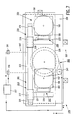
- the further positioning device 179 is shown diagrammatically in Fig. 7.
- the mask holders 181 and 183 of the further positioning device 179 are displaceably guided parallel to the X-direction and parallel to the Y-direction over a common guiding surface 199 of a support body 201 extending parallel to the X-direction and parallel to the Y-direction by means of an aerostatically supported foot 195 and an aerostatically supported foot 197, respectively.
- the support body 201 is fastened via a rotatable unit 203 to a balancing unit 205 which is displaceably guided, seen parallel to the X-direction and parallel to the Y-direction, by means of static gas bearings over a guiding surface 207 which forms part of a base 209 of the further positioning device 179.
- a guiding surface 207 which forms part of a base 209 of the further positioning device 179.
- the base 209 of the further positioning device 179 is fastened to the frame 1 of the lithographic device.
- the rotatable unit 203 and the balancing unit 205 of the further positioning device 179 correspond substantially to the rotatable unit 65 and the balancing unit 69 of the positioning device 3 described earlier.
- the first displacement unit 189 and the second displacement unit 191 of the further positioning device 179 each comprise an X-actuator 211 and 213 which is constructed as a force actuator.
- the X-actuators 211 and 213 each comprise a first part 215 and 217 which is displaceable, seen parallel to the X-direction, relative to a second part 219, 221 of the relevant X-actuator 211, 213 which extends substantially parallel to the X-direction.
- the second parts 219 and 221 of the X-actuators 211 and 213 are fastened to the support body 201 and comprise a common straight guide 223 which extends substantially parallel to the X-direction.
- the displacement units 189 and 191 each comprise an XY Lorentz force actuator 225, 227 with a permanent magnet system 229, 231 which is fastened to the mask holder 181, 183 of the relevant displacement unit 189, 191, and an electric coil system 233, 235 which is fastened to the first part 215, 217 of the X-actuator 211, 213 of the relevant displacement unit 189, 191.
- the mask holders 181 and 183 can be displaced parallel to the X-direction relative to the base 209 over comparatively great distances and with comparatively low accuracies by means of the X-actuators 211 and 213, while the mask holders 181 and 183 can be displaced relative to the first parts 215 and 217 of the X-actuators 211, 213 parallel to the X-direction and the Y-direction over comparatively small distances and with comparatively high accuracies by means of the XY Lorentz force actuators 225 and 227, and are rotatable through limited angles about an axis of rotation directed parallel to the Z-direction relative to said first parts 215 and 217.
- the positioning device 179 has a control unit 237, as does the positioning device 3, by means of which the straight guide 223 is held in a position parallel to the X-direction during operation, except for those moments in which the support body 201 is rotated through 180° relative to the base 209 by means of the rotatable unit 203, As Fig. 7 diagrammatically shows, the control unit 237 cooperates with two optical position sensors 239 and 241, and the control unit 237 controls an electric motor 243 of the rotatable unit 203.
- a batch of semiconductor substrates under manufacture is irradiated consecutively with a certain mask, whereupon said batch is irradiated consecutively with a next mask.
- the use of the positioning device 3, 97 according to the invention for the displacement of the semiconductor substrates achieves a considerable increase in the manufacturing output of the lithographic device, which manufacturing output is further increased through the use of the further positioning device 179 according to the invention for the displacement of the masks. It is noted that the invention also applies to lithographic devices in which a semiconductor substrate under manufacture is consecutively irradiated with a series of masks, whereupon a next semiconductor substrate is irradiated with said series of masks.
- a major increase in the manufacturing output of the lithographic device is achieved already in such a lithographic device if exclusively the positioning device for the displacement of the masks is a positioning device according to the invention, while the positioning device for the displacement of the semiconductor substrates is a conventional positioning device.
- lithographic devices according to the invention described above are used for exposing semiconductor substrates in the manufacture of integrated electronic semiconductor circuits. It is noted that such a lithographic device may also be used in the manufacture of other products provided with structures having detail dimensions in the sub-micron range, where mask patterns are imaged on a substrate by means of the lithographic device. Examples of this are structures of integrated optical systems, or conduction and detection patterns of magnetic domain memories, as well as structures of liquid crystal image display patterns.
- a positioning device may be used not only in a lithographic device but also in finishing machines, machine tools, and other machines or devices in which an object to be processed is aligned relative to an object holder in a measuring position and is subsequently processed in an operational position.
- the displacement units 25 and 27 of the positioning device 3 according to the invention as described above each comprise an X-actuator 39, 41 and a Y-actuator 43, 45.
- the displacement units 25, 27 of the positioning device 97 according to the invention as described above each comprise an X-actuator 105, 107, two Y-actuators 109, 111 and 113, 115, as well as an XY Lorentz force actuator 151, 153.
- the displacement units 189, 191 of the positioning device 179 according to the invention as described above each comprise an X-actuator 211, 213 and an XY Lorentz force actuator 225, 227. It is noted that a positioning device according to the invention may also be provided with an alternative type of displacement unit.
- linear X-actuators and Y-actuators mentioned above may be replaced by so-called planar electromagnetic motors which are usual and known per se.
- Such XYZ Lorentz force actuators may also be used, for
Landscapes
- Physics & Mathematics (AREA)
- General Physics & Mathematics (AREA)
- Engineering & Computer Science (AREA)
- Mechanical Engineering (AREA)
- Health & Medical Sciences (AREA)
- Environmental & Geological Engineering (AREA)
- Public Health (AREA)
- Epidemiology (AREA)
- Life Sciences & Earth Sciences (AREA)
- Toxicology (AREA)
- Atmospheric Sciences (AREA)
- Library & Information Science (AREA)
- Chemical & Material Sciences (AREA)
- Chemical Kinetics & Catalysis (AREA)
- Computer Networks & Wireless Communication (AREA)
- Exposure And Positioning Against Photoresist Photosensitive Materials (AREA)
- Container, Conveyance, Adherence, Positioning, Of Wafer (AREA)
- Exposure Of Semiconductors, Excluding Electron Or Ion Beam Exposure (AREA)
- Machine Tool Units (AREA)
- Shielding Devices Or Components To Electric Or Magnetic Fields (AREA)
- Devices For Indicating Variable Information By Combining Individual Elements (AREA)
Priority Applications (1)
| Application Number | Priority Date | Filing Date | Title |
|---|---|---|---|
| EP01126286A EP1197801B1 (de) | 1996-12-24 | 1997-10-03 | Lithographisches Gerät mit zwei Objekthaltern |
Applications Claiming Priority (6)
| Application Number | Priority Date | Filing Date | Title |
|---|---|---|---|
| EP96203709 | 1996-12-24 | ||
| EP96203709 | 1996-12-24 | ||
| EP97200706 | 1997-03-10 | ||
| EP97200706 | 1997-03-10 | ||
| EP97941149A EP0890136B9 (de) | 1996-12-24 | 1997-10-03 | In zwei richtungen ausgewogenes positioniergerät, sowie lithographisches gerät mit einem solchen positioniergerät |
| EP01126286A EP1197801B1 (de) | 1996-12-24 | 1997-10-03 | Lithographisches Gerät mit zwei Objekthaltern |
Related Parent Applications (1)
| Application Number | Title | Priority Date | Filing Date |
|---|---|---|---|
| EP97941149A Division EP0890136B9 (de) | 1996-12-24 | 1997-10-03 | In zwei richtungen ausgewogenes positioniergerät, sowie lithographisches gerät mit einem solchen positioniergerät |
Publications (2)
| Publication Number | Publication Date |
|---|---|
| EP1197801A1 true EP1197801A1 (de) | 2002-04-17 |
| EP1197801B1 EP1197801B1 (de) | 2005-12-28 |
Family
ID=26143490
Family Applications (2)
| Application Number | Title | Priority Date | Filing Date |
|---|---|---|---|
| EP01126286A Expired - Lifetime EP1197801B1 (de) | 1996-12-24 | 1997-10-03 | Lithographisches Gerät mit zwei Objekthaltern |
| EP97941149A Expired - Lifetime EP0890136B9 (de) | 1996-12-24 | 1997-10-03 | In zwei richtungen ausgewogenes positioniergerät, sowie lithographisches gerät mit einem solchen positioniergerät |
Family Applications After (1)
| Application Number | Title | Priority Date | Filing Date |
|---|---|---|---|
| EP97941149A Expired - Lifetime EP0890136B9 (de) | 1996-12-24 | 1997-10-03 | In zwei richtungen ausgewogenes positioniergerät, sowie lithographisches gerät mit einem solchen positioniergerät |
Country Status (6)
| Country | Link |
|---|---|
| US (1) | US5969441A (de) |
| EP (2) | EP1197801B1 (de) |
| JP (2) | JP2000505958A (de) |
| KR (1) | KR100512450B1 (de) |
| DE (2) | DE69735016T2 (de) |
| WO (1) | WO1998028665A1 (de) |
Cited By (4)
| Publication number | Priority date | Publication date | Assignee | Title |
|---|---|---|---|---|
| EP1862856A1 (de) * | 2006-05-31 | 2007-12-05 | ASML Netherlands BV | Messwerkzeug, System mit einer lithographischen Vorrichtung und einem Messwerkzeug und Verfahren zum Bestimmen eines Parameters eines Substrats |
| CN1952787B (zh) * | 2005-10-18 | 2010-09-01 | 国际商业机器公司 | 用于制造集成电路器件的方法和系统 |
| WO2012168272A1 (en) | 2011-06-08 | 2012-12-13 | Carl Zeiss Smt Gmbh | Measuring system |
| WO2017144277A1 (en) * | 2016-02-24 | 2017-08-31 | Asml Netherlands B.V. | Substrate handling system and lithographic apparatus |
Families Citing this family (667)
| Publication number | Priority date | Publication date | Assignee | Title |
|---|---|---|---|---|
| US5528118A (en) * | 1994-04-01 | 1996-06-18 | Nikon Precision, Inc. | Guideless stage with isolated reaction stage |
| JPH10209039A (ja) | 1997-01-27 | 1998-08-07 | Nikon Corp | 投影露光方法及び投影露光装置 |
| EP0900412B1 (de) * | 1997-03-10 | 2005-04-06 | ASML Netherlands B.V. | Lithographiegerät mit einer positioniervorrichtung mit zwei objekthaltern |
| JPH10270535A (ja) * | 1997-03-25 | 1998-10-09 | Nikon Corp | 移動ステージ装置、及び該ステージ装置を用いた回路デバイス製造方法 |
| IL135139A0 (en) | 1997-09-19 | 2001-05-20 | Nikon Corp | Stage apparatus, scanning type exposure apparatus, and device produced with the same |
| TW448487B (en) | 1997-11-22 | 2001-08-01 | Nippon Kogaku Kk | Exposure apparatus, exposure method and manufacturing method of device |
| DE69933903T2 (de) * | 1998-04-14 | 2007-05-24 | Asml Netherlands B.V. | Lithograpischer Projektionsapparat und Verfahren zur Herstellung einer Vorrichtung |
| EP0957275A3 (de) | 1998-05-14 | 2000-12-06 | Asm Lithography B.V. | Gaslager und solch ein Lager aufweisende lithographische Einrichtung |
| EP1134793A4 (de) * | 1998-06-17 | 2006-07-26 | Nikon Corp | Belichtungsmethode und belichtungsapparat |
| US6924884B2 (en) | 1999-03-08 | 2005-08-02 | Asml Netherlands B.V. | Off-axis leveling in lithographic projection apparatus |
| US7116401B2 (en) * | 1999-03-08 | 2006-10-03 | Asml Netherlands B.V. | Lithographic projection apparatus using catoptrics in an optical sensor system, optical arrangement, method of measuring, and device manufacturing method |
| TW490596B (en) * | 1999-03-08 | 2002-06-11 | Asm Lithography Bv | Lithographic projection apparatus, method of manufacturing a device using the lithographic projection apparatus, device manufactured according to the method and method of calibrating the lithographic projection apparatus |
| TWI242111B (en) | 1999-04-19 | 2005-10-21 | Asml Netherlands Bv | Gas bearings for use in vacuum chambers and their application in lithographic projection apparatus |
| TW513617B (en) | 1999-04-21 | 2002-12-11 | Asml Corp | Lithographic projection apparatus and method of manufacturing a device using a lithographic projection apparatus |
| TWI267704B (en) * | 1999-07-02 | 2006-12-01 | Asml Netherlands Bv | Capping layer for EUV optical elements |
| TW587199B (en) | 1999-09-29 | 2004-05-11 | Asml Netherlands Bv | Lithographic method and apparatus |
| JP2001118773A (ja) * | 1999-10-18 | 2001-04-27 | Nikon Corp | ステージ装置及び露光装置 |
| JP2001160530A (ja) | 1999-12-01 | 2001-06-12 | Nikon Corp | ステージ装置及び露光装置 |
| DE60032568T2 (de) * | 1999-12-01 | 2007-10-04 | Asml Netherlands B.V. | Positionierungsapparat und damit versehener lithographischer Apparat |
| TW546551B (en) | 1999-12-21 | 2003-08-11 | Asml Netherlands Bv | Balanced positioning system for use in lithographic apparatus |
| EP1111470B1 (de) * | 1999-12-21 | 2007-03-07 | ASML Netherlands B.V. | Lithographischer Apparat mit einem ausbalancierten Positionierungssystem |
| TW538256B (en) | 2000-01-14 | 2003-06-21 | Zeiss Stiftung | Microlithographic reduction projection catadioptric objective |
| TWI240849B (en) * | 2000-02-10 | 2005-10-01 | Asml Netherlands Bv | Object positioning method for a lithographic projection apparatus |
| TW588222B (en) * | 2000-02-10 | 2004-05-21 | Asml Netherlands Bv | Cooling of voice coil motors in lithographic projection apparatus |
| DE10006527A1 (de) * | 2000-02-15 | 2001-08-23 | Infineon Technologies Ag | Halbautomat zum halbautomatischen Abziehen von UV- Folie |
| US7301605B2 (en) | 2000-03-03 | 2007-11-27 | Nikon Corporation | Projection exposure apparatus and method, catadioptric optical system and manufacturing method of devices |
| JP2001257143A (ja) | 2000-03-09 | 2001-09-21 | Nikon Corp | ステージ装置及び露光装置、並びにデバイス製造方法 |
| US6437463B1 (en) * | 2000-04-24 | 2002-08-20 | Nikon Corporation | Wafer positioner with planar motor and mag-lev fine stage |
| US7508487B2 (en) * | 2000-06-01 | 2009-03-24 | Asml Netherlands B.V. | Lithographic apparatus, device manufacturing method, and device manufactured thereby |
| JP4474020B2 (ja) * | 2000-06-23 | 2010-06-02 | キヤノン株式会社 | 移動装置及び露光装置 |
| US6630984B2 (en) * | 2000-08-03 | 2003-10-07 | Asml Netherlands B.V. | Lithographic apparatus, device manufacturing method, and device manufactured thereby |
| US7561270B2 (en) | 2000-08-24 | 2009-07-14 | Asml Netherlands B.V. | Lithographic apparatus, device manufacturing method and device manufactured thereby |
| TW527526B (en) * | 2000-08-24 | 2003-04-11 | Asml Netherlands Bv | Lithographic apparatus, device manufacturing method, and device manufactured thereby |
| TWI232356B (en) | 2000-09-04 | 2005-05-11 | Asml Netherlands Bv | Lithographic projection apparatus, device manufacturing method and device manufactured thereby |
| TW548524B (en) * | 2000-09-04 | 2003-08-21 | Asm Lithography Bv | Lithographic projection apparatus, device manufacturing method and device manufactured thereby |
| EP1197803B1 (de) | 2000-10-10 | 2012-02-01 | ASML Netherlands B.V. | Lithographischer Apparat |
| EP2081086B1 (de) | 2000-11-07 | 2013-01-02 | ASML Netherlands B.V. | Lithografische Vorrichtung und Vorrichtungsherstellungsverfahren |
| US6603531B1 (en) | 2000-11-16 | 2003-08-05 | Nikon Corporation | Stage assembly including a reaction assembly that is connected by actuators |
| US6885430B2 (en) | 2000-11-16 | 2005-04-26 | Nikon Corporation | System and method for resetting a reaction mass assembly of a stage assembly |
| US6958808B2 (en) | 2000-11-16 | 2005-10-25 | Nikon Corporation | System and method for resetting a reaction mass assembly of a stage assembly |
| US6593997B1 (en) * | 2000-11-16 | 2003-07-15 | Nikon Corporation | Stage assembly including a reaction assembly |
| US6757053B1 (en) | 2000-11-16 | 2004-06-29 | Nikon Corporation | Stage assembly including a reaction mass assembly |
| TW591342B (en) * | 2000-11-30 | 2004-06-11 | Asml Netherlands Bv | Lithographic projection apparatus and integrated circuit manufacturing method using a lithographic projection apparatus |
| US7113258B2 (en) * | 2001-01-15 | 2006-09-26 | Asml Netherlands B.V. | Lithographic apparatus |
| US6987558B2 (en) | 2001-01-16 | 2006-01-17 | Nikon Corporation | Reaction mass for a stage device |
| US6927838B2 (en) | 2001-02-27 | 2005-08-09 | Nikon Corporation | Multiple stage, stage assembly having independent stage bases |
| US20020117109A1 (en) * | 2001-02-27 | 2002-08-29 | Hazelton Andrew J. | Multiple stage, stage assembly having independent reaction force transfer |
| US6792591B2 (en) * | 2001-02-28 | 2004-09-14 | Asml Masktools B.V. | Method of identifying an extreme interaction pitch region, methods of designing mask patterns and manufacturing masks, device manufacturing methods and computer programs |
| KR100597035B1 (ko) * | 2001-03-01 | 2006-07-04 | 에이에스엠엘 네델란즈 비.브이. | 마스크핸들링방법, 마스크, 그를 위한 그리퍼를 포함하는기구 또는 장치, 디바이스 제조방법 및 그 디바이스 |
| JP4267245B2 (ja) | 2001-03-14 | 2009-05-27 | エーエスエムエル マスクツールズ ビー.ブイ. | 解像度以下の補助フィーチャとして罫線ラダー・バーを利用した光近接補正方法 |
| US7735052B2 (en) * | 2001-04-24 | 2010-06-08 | Asml Masktools Netherlands B.V. | Method of identifying an extreme interaction pitch region, methods of designing mask patterns and manufacturing masks, device manufacturing methods and computer programs |
| JP4814438B2 (ja) * | 2001-05-02 | 2011-11-16 | 日本トムソン株式会社 | リニアモータを内蔵したステージ装置 |
| TWI253682B (en) | 2001-05-23 | 2006-04-21 | Asml Netherlands Bv | Substrate provided with an alignment mark, method of designing a mask, computer program, mask for exposing said mark, device manufacturing method, and device manufactured thereby |
| JP2003059827A (ja) * | 2001-06-20 | 2003-02-28 | Asml Netherlands Bv | デバイスを製造する方法、この方法によって製造したデバイス、およびこの方法で使用するマスク |
| US6788385B2 (en) * | 2001-06-21 | 2004-09-07 | Nikon Corporation | Stage device, exposure apparatus and method |
| US6903346B2 (en) * | 2001-07-11 | 2005-06-07 | Nikon Corporation | Stage assembly having a follower assembly |
| TW529172B (en) * | 2001-07-24 | 2003-04-21 | Asml Netherlands Bv | Imaging apparatus |
| US6674512B2 (en) | 2001-08-07 | 2004-01-06 | Nikon Corporation | Interferometer system for a semiconductor exposure system |
| US6785005B2 (en) | 2001-09-21 | 2004-08-31 | Nikon Corporation | Switching type dual wafer stage |
| US7026081B2 (en) * | 2001-09-28 | 2006-04-11 | Asml Masktools B.V. | Optical proximity correction method utilizing phase-edges as sub-resolution assist features |
| JP3980469B2 (ja) * | 2001-10-19 | 2007-09-26 | エーエスエムエル ネザーランズ ビー.ブイ. | リソグラフィック装置及びデバイス製造方法 |
| US6665054B2 (en) | 2001-10-22 | 2003-12-16 | Nikon Corporation | Two stage method |
| KR100436213B1 (ko) * | 2001-12-17 | 2004-06-16 | 미래산업 주식회사 | 반도체 소자 테스트 핸들러용 소자 정렬장치 |
| US6927505B2 (en) | 2001-12-19 | 2005-08-09 | Nikon Corporation | Following stage planar motor |
| US7002668B2 (en) * | 2002-03-08 | 2006-02-21 | Rivin Eugeny I | Stage positioning unit for photo lithography tool and for the like |
| US7170587B2 (en) * | 2002-03-18 | 2007-01-30 | Asml Netherlands B.V. | Lithographic apparatus and device manufacturing method |
| US7333178B2 (en) * | 2002-03-18 | 2008-02-19 | Asml Netherlands B.V. | Lithographic apparatus and device manufacturing method |
| US7061577B2 (en) | 2002-03-26 | 2006-06-13 | Nikon Corporation | Image adjustor including damping assembly |
| US6724466B2 (en) | 2002-03-26 | 2004-04-20 | Nikon Corporation | Stage assembly including a damping assembly |
| EP1367446A1 (de) | 2002-05-31 | 2003-12-03 | ASML Netherlands B.V. | Lithographischer Apparat |
| EP1383007A1 (de) * | 2002-07-16 | 2004-01-21 | ASML Netherlands B.V. | Lithographischer Apparat und Verfahren zur Herstellung einer Vorrichtung |
| US6859259B2 (en) * | 2002-08-15 | 2005-02-22 | Asml Netherlands B.V. | Lithographic projection apparatus and reflector assembly for use therein |
| EP1400860B1 (de) | 2002-09-20 | 2013-11-06 | ASML Netherlands B.V. | Lithographische Markierungsstruktur, lithographischer Projektionsapparat mit einer solchen Markierungsstruktur und Verfahren zur Ausrichtung eines Substrates unter Verwendung einer solchen Markierungsstruktur |
| JP4222927B2 (ja) * | 2002-09-20 | 2009-02-12 | エーエスエムエル ネザーランズ ビー.ブイ. | 少なくとも2波長を使用するリソグラフィ装置用アライメント・システム |
| TWI246114B (en) * | 2002-09-24 | 2005-12-21 | Asml Netherlands Bv | Lithographic apparatus, device manufacturing method, and device manufactured thereby |
| TWI250387B (en) * | 2002-09-30 | 2006-03-01 | Asml Netherlands Bv | Lithographic apparatus and device manufacturing method |
| SG128447A1 (en) * | 2002-09-30 | 2007-01-30 | Asml Netherlands Bv | Lithographic apparatus and device manufacturing method |
| US7110081B2 (en) * | 2002-11-12 | 2006-09-19 | Asml Netherlands B.V. | Lithographic apparatus and device manufacturing method |
| US10503084B2 (en) | 2002-11-12 | 2019-12-10 | Asml Netherlands B.V. | Lithographic apparatus and device manufacturing method |
| SG137657A1 (en) * | 2002-11-12 | 2007-12-28 | Asml Masktools Bv | Method and apparatus for performing model-based layout conversion for use with dipole illumination |
| EP1420298B1 (de) | 2002-11-12 | 2013-02-20 | ASML Netherlands B.V. | Lithographischer Apparat |
| EP1429188B1 (de) | 2002-11-12 | 2013-06-19 | ASML Netherlands B.V. | Lithographischer Projektionsapparat |
| SG121819A1 (en) | 2002-11-12 | 2006-05-26 | Asml Netherlands Bv | Lithographic apparatus and device manufacturing method |
| SG121822A1 (en) * | 2002-11-12 | 2006-05-26 | Asml Netherlands Bv | Lithographic apparatus and device manufacturing method |
| SG116510A1 (de) * | 2002-11-12 | 2005-11-28 | ||
| US9482966B2 (en) | 2002-11-12 | 2016-11-01 | Asml Netherlands B.V. | Lithographic apparatus and device manufacturing method |
| EP1420302A1 (de) | 2002-11-18 | 2004-05-19 | ASML Netherlands B.V. | Lithographischer Apparat und Verfahren zur Herstellung einer Vorrichtung |
| SG111171A1 (en) * | 2002-11-27 | 2005-05-30 | Asml Netherlands Bv | Lithographic projection apparatus and device manufacturing method |
| SG115590A1 (en) * | 2002-11-27 | 2005-10-28 | Asml Netherlands Bv | Lithographic projection apparatus and device manufacturing method |
| TW200412617A (en) * | 2002-12-03 | 2004-07-16 | Nikon Corp | Optical illumination device, method for adjusting optical illumination device, exposure device and exposure method |
| JP4525062B2 (ja) * | 2002-12-10 | 2010-08-18 | 株式会社ニコン | 露光装置及びデバイス製造方法、露光システム |
| EP1571700A4 (de) | 2002-12-10 | 2007-09-12 | Nikon Corp | Optische vorrichtung und projektionsbelichtungsvorrichtung unter verwendung der optischen vorrichtung |
| US7242455B2 (en) * | 2002-12-10 | 2007-07-10 | Nikon Corporation | Exposure apparatus and method for producing device |
| SG171468A1 (en) * | 2002-12-10 | 2011-06-29 | Nikon Corp | Exposure apparatus and method for producing device |
| DE60323927D1 (de) * | 2002-12-13 | 2008-11-20 | Asml Netherlands Bv | Lithographischer Apparat und Verfahren zur Herstellung einer Vorrichtung |
| SG123589A1 (en) * | 2002-12-19 | 2006-07-26 | Asml Netherlands Bv | A lithographic projection mask, a device manufacturing method using a lithographic projection mask and a device manufactured thereby |
| EP1431825A1 (de) * | 2002-12-20 | 2004-06-23 | ASML Netherlands B.V. | Lithographischer Apparat, Verfahren zur Herstellung einer Vorrichtung und Substrathalter |
| DE10261775A1 (de) | 2002-12-20 | 2004-07-01 | Carl Zeiss Smt Ag | Vorrichtung zur optischen Vermessung eines Abbildungssystems |
| CN100476585C (zh) * | 2002-12-23 | 2009-04-08 | Asml荷兰有限公司 | 具有可扩展薄片的杂质屏蔽 |
| EP1434092A1 (de) | 2002-12-23 | 2004-06-30 | ASML Netherlands B.V. | Lithographischer Apparat, Verfahren zur Herstellung eines Artikels und damit erzeugter Artikel |
| TWI286674B (en) * | 2002-12-27 | 2007-09-11 | Asml Netherlands Bv | Container for a mask, method of transferring lithographic masks therein and method of scanning a mask in a container |
| SG139530A1 (en) * | 2003-01-14 | 2008-02-29 | Asml Masktools Bv | Method of optical proximity correction design for contact hole mask |
| SG125101A1 (en) * | 2003-01-14 | 2006-09-29 | Asml Netherlands Bv | Level sensor for lithographic apparatus |
| TWI304158B (en) * | 2003-01-15 | 2008-12-11 | Asml Netherlands Bv | Detection assembly and lithographic projection apparatus provided with such a detection assembly |
| US6963821B2 (en) * | 2003-02-11 | 2005-11-08 | Nikon Corporation | Stage counter mass system |
| US7151981B2 (en) * | 2003-02-20 | 2006-12-19 | Applied Materials, Inc. | Methods and apparatus for positioning a substrate relative to a support stage |
| US7499767B2 (en) * | 2003-02-20 | 2009-03-03 | Applied Materials, Inc. | Methods and apparatus for positioning a substrate relative to a support stage |
| JP4615877B2 (ja) * | 2003-02-20 | 2011-01-19 | アプライド マテリアルズ インコーポレイテッド | 支持ステージに対して基板を位置決めする装置及びコンピュータプログラム |
| EP2466621B1 (de) | 2003-02-26 | 2015-04-01 | Nikon Corporation | Belichtungsvorrichtung, Belichtungsverfahren und Verfahren zur Herstellung des Geräts |
| US7206059B2 (en) * | 2003-02-27 | 2007-04-17 | Asml Netherlands B.V. | Stationary and dynamic radial transverse electric polarizer for high numerical aperture systems |
| US6943941B2 (en) * | 2003-02-27 | 2005-09-13 | Asml Netherlands B.V. | Stationary and dynamic radial transverse electric polarizer for high numerical aperture systems |
| SG115641A1 (en) * | 2003-03-06 | 2005-10-28 | Asml Netherlands Bv | Device and method for manipulation and routing of a metrology beam |
| TWI264620B (en) * | 2003-03-07 | 2006-10-21 | Asml Netherlands Bv | Lithographic apparatus and device manufacturing method |
| SG123601A1 (en) | 2003-03-10 | 2006-07-26 | Asml Netherlands Bv | Focus spot monitoring in a lithographic projectionapparatus |
| SG115630A1 (en) * | 2003-03-11 | 2005-10-28 | Asml Netherlands Bv | Temperature conditioned load lock, lithographic apparatus comprising such a load lock and method of manufacturing a substrate with such a load lock |
| TWI234692B (en) * | 2003-03-11 | 2005-06-21 | Asml Netherlands Bv | Lithographic projection assembly, handling apparatus for handling substrates and method of handling a substrate |
| EP1457825A1 (de) * | 2003-03-11 | 2004-09-15 | ASML Netherlands B.V. | Lithographischer Apparat, Verfahren zur Herstellung eines Artikels und damit erzeugter Artikel |
| SG115631A1 (en) * | 2003-03-11 | 2005-10-28 | Asml Netherlands Bv | Lithographic projection assembly, load lock and method for transferring objects |
| EP1457827A1 (de) * | 2003-03-11 | 2004-09-15 | ASML Netherlands B.V. | Lithographischer Apparat, Verfahren zur Herstellung eines Artikels und damit erzeugter Artikel |
| SG125108A1 (en) * | 2003-03-11 | 2006-09-29 | Asml Netherlands Bv | Assembly comprising a sensor for determining at least one of tilt and height of a substrate, a method therefor and a lithographic projection apparatus |
| SG115629A1 (en) * | 2003-03-11 | 2005-10-28 | Asml Netherlands Bv | Method and apparatus for maintaining a machine part |
| EP1457826A1 (de) * | 2003-03-11 | 2004-09-15 | ASML Netherlands B.V. | Lithographischer Apparat und Verfahren zur Herstellung eines Artikels |
| EP1457833B1 (de) | 2003-03-11 | 2012-05-30 | ASML Netherlands B.V. | Lithographischer Apparat, Verfahren zur Herstellung eines Artikels und damit erzeugter Artikel |
| KR101181688B1 (ko) | 2003-03-25 | 2012-09-19 | 가부시키가이샤 니콘 | 노광 장치 및 디바이스 제조 방법 |
| US7397539B2 (en) * | 2003-03-31 | 2008-07-08 | Asml Netherlands, B.V. | Transfer apparatus for transferring an object, lithographic apparatus employing such a transfer apparatus, and method of use thereof |
| SG125948A1 (en) * | 2003-03-31 | 2006-10-30 | Asml Netherlands Bv | Supporting structure for use in a lithographic apparatus |
| KR100760037B1 (ko) * | 2003-03-31 | 2007-09-20 | 에이에스엠엘 마스크툴즈 비.브이. | 소스 및 마스크 최적화 방법 |
| US7126671B2 (en) * | 2003-04-04 | 2006-10-24 | Asml Netherlands B.V. | Lithographic apparatus and device manufacturing method |
| JP4902201B2 (ja) | 2003-04-07 | 2012-03-21 | 株式会社ニコン | 露光装置、露光方法及びデバイス製造方法 |
| JP4394500B2 (ja) * | 2003-04-09 | 2010-01-06 | エーエスエムエル ネザーランズ ビー.ブイ. | リソグラフィ装置、デバイス製造方法、及びコンピュータ・プログラム |
| KR20170018113A (ko) | 2003-04-09 | 2017-02-15 | 가부시키가이샤 니콘 | 노광 방법 및 장치, 그리고 디바이스 제조 방법 |
| WO2004090634A2 (en) | 2003-04-10 | 2004-10-21 | Nikon Corporation | Environmental system including vaccum scavange for an immersion lithography apparatus |
| KR101177330B1 (ko) | 2003-04-10 | 2012-08-30 | 가부시키가이샤 니콘 | 액침 리소그래피 장치 |
| KR20170016014A (ko) | 2003-04-11 | 2017-02-10 | 가부시키가이샤 니콘 | 액침 리소그래피에 의한 광학기기의 세정방법 |
| KR101159564B1 (ko) | 2003-04-11 | 2012-06-25 | 가부시키가이샤 니콘 | 액침 리소그래피 머신에서 웨이퍼 교환동안 투영 렌즈 아래의 갭에서 액침액체를 유지하는 장치 및 방법 |
| JP4071733B2 (ja) | 2003-04-17 | 2008-04-02 | エーエスエムエル ネザーランズ ビー.ブイ. | リソグラフィ装置、デバイス製造方法、およびコンピュータ・プログラム |
| JP4315420B2 (ja) | 2003-04-18 | 2009-08-19 | キヤノン株式会社 | 露光装置及び露光方法 |
| SG115678A1 (en) | 2003-04-22 | 2005-10-28 | Asml Netherlands Bv | Substrate carrier and method for making a substrate carrier |
| TWI237307B (en) * | 2003-05-01 | 2005-08-01 | Nikon Corp | Optical projection system, light exposing apparatus and light exposing method |
| US7348575B2 (en) | 2003-05-06 | 2008-03-25 | Nikon Corporation | Projection optical system, exposure apparatus, and exposure method |
| EP1475666A1 (de) | 2003-05-06 | 2004-11-10 | ASML Netherlands B.V. | Substrathalter für einen lithographischen Apparat |
| SG10201405231YA (en) | 2003-05-06 | 2014-09-26 | Nippon Kogaku Kk | Projection optical system, exposure apparatus, and exposure method |
| EP1475667A1 (de) * | 2003-05-09 | 2004-11-10 | ASML Netherlands B.V. | Lithographischer Apparat und Verfahren zur Herstellung einer Vorrichtung |
| US20040263816A1 (en) * | 2003-05-12 | 2004-12-30 | Asml Netherlands B.V. | Lithographic apparatus and device manufacturing method |
| EP1477861A1 (de) * | 2003-05-16 | 2004-11-17 | ASML Netherlands B.V. | Verfahren zur Eichung eines lithographischen Geräts, Ausrichtverfahren, Komputerprogramm, lithographisches Gerät und Verfahren zur Herstellung einer Vorrichtung |
| SG141228A1 (en) * | 2003-05-19 | 2008-04-28 | Asml Netherlands Bv | Lithographic apparatus and device manufacturing method |
| TWI421911B (zh) | 2003-05-23 | 2014-01-01 | 尼康股份有限公司 | An exposure method, an exposure apparatus, and an element manufacturing method |
| TWI424470B (zh) | 2003-05-23 | 2014-01-21 | 尼康股份有限公司 | A method of manufacturing an exposure apparatus and an element |
| CN100541717C (zh) | 2003-05-28 | 2009-09-16 | 株式会社尼康 | 曝光方法、曝光装置以及器件制造方法 |
| TWI347741B (en) * | 2003-05-30 | 2011-08-21 | Asml Netherlands Bv | Lithographic apparatus and device manufacturing method |
| US7213963B2 (en) | 2003-06-09 | 2007-05-08 | Asml Netherlands B.V. | Lithographic apparatus and device manufacturing method |
| EP1486828B1 (de) | 2003-06-09 | 2013-10-09 | ASML Netherlands B.V. | Lithographischer Apparat und Verfahren zur Herstellung einer Vorrichtung |
| US7317504B2 (en) * | 2004-04-08 | 2008-01-08 | Asml Netherlands B.V. | Lithographic apparatus and device manufacturing method |
| US20040252287A1 (en) * | 2003-06-11 | 2004-12-16 | Michael Binnard | Reaction frame assembly that functions as a reaction mass |
| EP2261742A3 (de) * | 2003-06-11 | 2011-05-25 | ASML Netherlands BV | Lithographischer Apparat und Verfahren zur Herstellung einer Vorrichtung |
| EP1486824A1 (de) * | 2003-06-11 | 2004-12-15 | ASML Netherlands B.V. | Bewegliches Trägersystem für einen lithographischen Belichtungsapparat, lithographischer Belichtungssapparat und Verfahren zur Herstellung einer Vorrichtung |
| KR101520591B1 (ko) | 2003-06-13 | 2015-05-14 | 가부시키가이샤 니콘 | 노광 방법, 기판 스테이지, 노광 장치, 및 디바이스 제조 방법 |
| TWI515770B (zh) | 2003-06-19 | 2016-01-01 | 尼康股份有限公司 | An exposure apparatus, an exposure method, and an element manufacturing method |
| EP1491967A1 (de) * | 2003-06-27 | 2004-12-29 | ASML Netherlands B.V. | Verfahren und Vorrichtung zur Positionierung eines Substrats auf einem Substrattisch |
| TWI251129B (en) * | 2003-06-27 | 2006-03-11 | Asml Netherlands Bv | Lithographic apparatus and integrated circuit manufacturing method |
| EP1975721A1 (de) | 2003-06-30 | 2008-10-01 | ASML Netherlands B.V. | Lithographischer Apparat und Verfahren zur Herstellung eines Artikels |
| JP4520787B2 (ja) * | 2003-06-30 | 2010-08-11 | エーエスエムエル マスクツールズ ビー.ブイ. | 半波長以下リソグラフィ模様付けの改良型散乱バーopc適用方法 |
| US7355673B2 (en) * | 2003-06-30 | 2008-04-08 | Asml Masktools B.V. | Method, program product and apparatus of simultaneous optimization for NA-Sigma exposure settings and scattering bars OPC using a device layout |
| SG144723A1 (en) | 2003-06-30 | 2008-08-28 | Asml Masktools Bv | A method, program product and apparatus for generating assist features utilizing an image field map |
| TWI284253B (en) * | 2003-07-01 | 2007-07-21 | Asml Netherlands Bv | Lithographic apparatus and device manufacturing method |
| US7248339B2 (en) * | 2003-07-04 | 2007-07-24 | Asml Netherlands B.V. | Lithographic apparatus and device manufacturing method |
| WO2005006418A1 (ja) | 2003-07-09 | 2005-01-20 | Nikon Corporation | 露光装置及びデバイス製造方法 |
| ATE513309T1 (de) * | 2003-07-09 | 2011-07-15 | Nikon Corp | Belichtungsvorrichtung und verfahren zur bauelementeherstellung |
| WO2005006416A1 (ja) * | 2003-07-09 | 2005-01-20 | Nikon Corporation | 結合装置、露光装置、及びデバイス製造方法 |
| EP1646074A4 (de) * | 2003-07-09 | 2007-10-03 | Nikon Corp | Belichtungsvorrichtung und verfahren zur bauelementeherstellung |
| EP1496397A1 (de) * | 2003-07-11 | 2005-01-12 | ASML Netherlands B.V. | Methode und System zur vorwärts gerichteten Overlay-Korrektur musterinduzierter Bildverzerrung- und verschiebung, und lithographisches Projektionsgerät zur Benutzung derselben |
| US7384149B2 (en) | 2003-07-21 | 2008-06-10 | Asml Netherlands B.V. | Lithographic projection apparatus, gas purging method and device manufacturing method and purge gas supply system |
| EP1500987A1 (de) * | 2003-07-21 | 2005-01-26 | ASML Netherlands B.V. | Lithographischer Apparat, Verfahren zur Herstellung eines Artikels und damit hergestellter Artikel |
| EP1500979A1 (de) * | 2003-07-21 | 2005-01-26 | ASML Netherlands B.V. | Lithographischer Apparat und Verfahren zur Herstellung eines Artikels |
| TWI245170B (en) | 2003-07-22 | 2005-12-11 | Asml Netherlands Bv | Lithographic apparatus, device manufacturing method, and device manufactured thereby |
| EP1500980A1 (de) * | 2003-07-22 | 2005-01-26 | ASML Netherlands B.V. | Lithographischer Projektionsapparat, Verfahren zur Herstellung eines Artikels und dabei erzeugter Artikel |
| JP4565915B2 (ja) * | 2003-07-23 | 2010-10-20 | エーエスエムエル ネザーランズ ビー.ブイ. | リソグラフィ投影装置及び物品保持器 |
| US7456932B2 (en) * | 2003-07-25 | 2008-11-25 | Asml Netherlands B.V. | Filter window, lithographic projection apparatus, filter window manufacturing method, device manufacturing method and device manufactured thereby |
| EP1503244A1 (de) | 2003-07-28 | 2005-02-02 | ASML Netherlands B.V. | Lithographischer Projektionsapparat und Verfahren zur Herstellung einer Vorrichtung |
| CN102043350B (zh) | 2003-07-28 | 2014-01-29 | 株式会社尼康 | 曝光装置、器件制造方法、及曝光装置的控制方法 |
| US7145643B2 (en) * | 2003-08-07 | 2006-12-05 | Asml Netherlands B.V. | Interface unit, lithographic projection apparatus comprising such an interface unit and a device manufacturing method |
| KR101381563B1 (ko) | 2003-08-21 | 2014-04-04 | 가부시키가이샤 니콘 | 노광 장치, 노광 방법 및 디바이스 제조 방법 |
| US8149381B2 (en) | 2003-08-26 | 2012-04-03 | Nikon Corporation | Optical element and exposure apparatus |
| EP2278402B1 (de) | 2003-08-26 | 2013-03-06 | Nikon Corporation | Belichtungsvorrichtung |
| US7265817B2 (en) * | 2003-08-27 | 2007-09-04 | Asml Netherlands B.V. | Lithographic apparatus, device manufacturing method, and slide assembly |
| TWI245163B (en) | 2003-08-29 | 2005-12-11 | Asml Netherlands Bv | Lithographic apparatus and device manufacturing method |
| EP3163375B1 (de) | 2003-08-29 | 2019-01-09 | Nikon Corporation | Belichtungsvorrichtung und belichtungsverfahren |
| US6954256B2 (en) | 2003-08-29 | 2005-10-11 | Asml Netherlands B.V. | Gradient immersion lithography |
| CN100407371C (zh) * | 2003-08-29 | 2008-07-30 | 株式会社尼康 | 曝光装置和器件加工方法 |
| US6873938B1 (en) | 2003-09-17 | 2005-03-29 | Asml Netherlands B.V. | Adaptive lithographic critical dimension enhancement |
| WO2005029559A1 (ja) * | 2003-09-19 | 2005-03-31 | Nikon Corporation | 露光装置及びデバイス製造方法 |
| US8064730B2 (en) * | 2003-09-22 | 2011-11-22 | Asml Netherlands B.V. | Device manufacturing method, orientation determination method and lithographic apparatus |
| US8208198B2 (en) | 2004-01-14 | 2012-06-26 | Carl Zeiss Smt Gmbh | Catadioptric projection objective |
| KR101248325B1 (ko) | 2003-09-26 | 2013-03-27 | 가부시키가이샤 니콘 | 투영노광장치 및 투영노광장치의 세정방법, 메인터넌스방법 그리고 디바이스의 제조방법 |
| CN1860585B (zh) * | 2003-09-29 | 2010-04-28 | 株式会社尼康 | 液浸型透镜系统和投影曝光装置 |
| KR101664642B1 (ko) | 2003-09-29 | 2016-10-11 | 가부시키가이샤 니콘 | 노광장치, 노광방법 및 디바이스 제조방법 |
| WO2005031824A1 (ja) * | 2003-09-29 | 2005-04-07 | Nikon Corporation | 投影露光装置、投影露光方法およびデバイス製造方法 |
| WO2005036621A1 (ja) | 2003-10-08 | 2005-04-21 | Zao Nikon Co., Ltd. | 基板搬送装置及び基板搬送方法、露光装置及び露光方法、デバイス製造方法 |
| TWI598934B (zh) | 2003-10-09 | 2017-09-11 | 尼康股份有限公司 | Exposure apparatus, exposure method, and device manufacturing method |
| DE602004030365D1 (de) | 2003-10-22 | 2011-01-13 | Nippon Kogaku Kk | Belichtungsvorrichtung, belichtungsverfahren und verfahren zur bauelementeherstellung |
| EP1679738A4 (de) | 2003-10-28 | 2008-08-06 | Nikon Corp | Belichtungsvorrichtung, belichtungsverfahren und bauelementeherstellungsverfahren |
| TW201834020A (zh) | 2003-10-28 | 2018-09-16 | 日商尼康股份有限公司 | 照明光學裝置、曝光裝置、曝光方法以及元件製造方法 |
| CN100461336C (zh) | 2003-10-31 | 2009-02-11 | 株式会社尼康 | 曝光装置以及器件制造方法 |
| US7665946B2 (en) * | 2003-11-04 | 2010-02-23 | Advanced Display Process Engineering Co., Ltd. | Transfer chamber for flat display device manufacturing apparatus |
| US7061579B2 (en) * | 2003-11-13 | 2006-06-13 | Asml Netherlands B.V. | Lithographic apparatus and device manufacturing method |
| WO2005048325A1 (ja) * | 2003-11-17 | 2005-05-26 | Nikon Corporation | ステージ駆動方法及びステージ装置並びに露光装置 |
| TW201809801A (zh) | 2003-11-20 | 2018-03-16 | 日商尼康股份有限公司 | 光學照明裝置、曝光裝置、曝光方法、以及元件製造方法 |
| US7414759B2 (en) * | 2003-11-26 | 2008-08-19 | Samsung Electronics Co., Ltd. | Scanner linearity tester |
| US7253077B2 (en) * | 2003-12-01 | 2007-08-07 | Asml Netherlands B.V. | Substrate, method of preparing a substrate, method of measurement, lithographic apparatus, device manufacturing method and device manufactured thereby, and machine-readable storage medium |
| EP2717295B1 (de) | 2003-12-03 | 2018-07-18 | Nikon Corporation | Belichtungsvorrichtung, Belichtungsverfahren, und Verfahren zur Herstellung einer Vorrichtung |
| US7565219B2 (en) * | 2003-12-09 | 2009-07-21 | Asml Netherlands B.V. | Lithographic apparatus, method of determining a model parameter, device manufacturing method, and device manufactured thereby |
| US7466489B2 (en) | 2003-12-15 | 2008-12-16 | Susanne Beder | Projection objective having a high aperture and a planar end surface |
| DE602004030481D1 (de) | 2003-12-15 | 2011-01-20 | Nippon Kogaku Kk | Bühnensystem, belichtungsvorrichtung und belichtungsverfahren |
| US20050134865A1 (en) * | 2003-12-17 | 2005-06-23 | Asml Netherlands B.V. | Method for determining a map, device manufacturing method, and lithographic apparatus |
| US7288779B2 (en) * | 2003-12-17 | 2007-10-30 | Asml Netherlands B.V. | Method for position determination, method for overlay optimization, and lithographic projection apparatus |
| WO2005059645A2 (en) | 2003-12-19 | 2005-06-30 | Carl Zeiss Smt Ag | Microlithography projection objective with crystal elements |
| US7113255B2 (en) | 2003-12-19 | 2006-09-26 | Asml Holding N.V. | Grating patch arrangement, lithographic apparatus, method of testing, device manufacturing method, and device manufactured thereby |
| US7460206B2 (en) | 2003-12-19 | 2008-12-02 | Carl Zeiss Smt Ag | Projection objective for immersion lithography |
| US7292315B2 (en) * | 2003-12-19 | 2007-11-06 | Asml Masktools B.V. | Optimized polarization illumination |
| US6955074B2 (en) * | 2003-12-29 | 2005-10-18 | Asml Netherlands, B.V. | Lithographic apparatus, method of calibration, calibration plate, device manufacturing method, and device manufactured thereby |
| US7349101B2 (en) * | 2003-12-30 | 2008-03-25 | Asml Netherlands B.V. | Lithographic apparatus, overlay detector, device manufacturing method, and device manufactured thereby |
| US7145641B2 (en) * | 2003-12-31 | 2006-12-05 | Asml Netherlands, B.V. | Lithographic apparatus, device manufacturing method, and device manufactured thereby |
| EP3376523A1 (de) | 2004-01-05 | 2018-09-19 | Nikon Corporation | Belichtungsvorrichtung, belichtungsverfahren und verfahren zur herstellung einer vorrichtung |
| CN1902733A (zh) * | 2004-01-06 | 2007-01-24 | 株式会社尼康 | 曝光方法和装置以及器件制造方法 |
| US20080151364A1 (en) | 2004-01-14 | 2008-06-26 | Carl Zeiss Smt Ag | Catadioptric projection objective |
| US7463422B2 (en) | 2004-01-14 | 2008-12-09 | Carl Zeiss Smt Ag | Projection exposure apparatus |
| KR101407204B1 (ko) | 2004-01-14 | 2014-06-13 | 칼 짜이스 에스엠티 게엠베하 | 투영 대물렌즈 |
| JP4710611B2 (ja) | 2004-01-15 | 2011-06-29 | 株式会社ニコン | 露光装置及びデバイスの製造方法並びに露光方法 |
| CN1938646B (zh) | 2004-01-20 | 2010-12-15 | 卡尔蔡司Smt股份公司 | 曝光装置和用于投影透镜的测量装置 |
| US7697110B2 (en) | 2004-01-26 | 2010-04-13 | Nikon Corporation | Exposure apparatus and device manufacturing method |
| TWI395068B (zh) * | 2004-01-27 | 2013-05-01 | 尼康股份有限公司 | 光學系統、曝光裝置以及曝光方法 |
| US7221433B2 (en) | 2004-01-28 | 2007-05-22 | Nikon Corporation | Stage assembly including a reaction assembly having a connector assembly |
| US7256873B2 (en) * | 2004-01-28 | 2007-08-14 | Asml Netherlands B.V. | Enhanced lithographic resolution through double exposure |
| US7589822B2 (en) | 2004-02-02 | 2009-09-15 | Nikon Corporation | Stage drive method and stage unit, exposure apparatus, and device manufacturing method |
| CN100552879C (zh) * | 2004-02-02 | 2009-10-21 | 尼康股份有限公司 | 载台驱动方法及载台装置、曝光装置、及元件制造方法 |
| EP1713114B1 (de) | 2004-02-03 | 2018-09-19 | Nikon Corporation | Belichtungsvorrichtung und verfahren zur herstellung einer vorrichtung |
| EP1713115B1 (de) | 2004-02-04 | 2016-05-04 | Nikon Corporation | Belichtungsvorrichtung, belichtungsverfahren und bauelementeherstellungsverfahren |
| TWI389174B (zh) | 2004-02-06 | 2013-03-11 | 尼康股份有限公司 | 偏光變換元件、光學照明裝置、曝光裝置以及曝光方法 |
| KR101166007B1 (ko) | 2004-02-10 | 2012-07-17 | 가부시키가이샤 니콘 | 노광 장치 및 디바이스 제조 방법, 메인터넌스 방법 및노광 방법 |
| US7113256B2 (en) * | 2004-02-18 | 2006-09-26 | Asml Netherlands B.V. | Lithographic apparatus and device manufacturing method with feed-forward focus control |
| US7352472B2 (en) * | 2004-02-18 | 2008-04-01 | Asml Netherlands B.V. | Lithographic apparatus, device manufacturing method, and method for determining z-displacement |
| SG132679A1 (en) * | 2004-02-19 | 2007-06-28 | Nikon Corp | Exposure apparatus, exposure method, and device fabricating method |
| US20070030467A1 (en) * | 2004-02-19 | 2007-02-08 | Nikon Corporation | Exposure apparatus, exposure method, and device fabricating method |
| WO2005081291A1 (ja) * | 2004-02-19 | 2005-09-01 | Nikon Corporation | 露光装置及びデバイスの製造方法 |
| KR101106497B1 (ko) | 2004-02-20 | 2012-01-20 | 가부시키가이샤 니콘 | 노광 장치, 공급 방법 및 회수 방법, 노광 방법, 및디바이스 제조 방법 |
| WO2005081295A1 (ja) * | 2004-02-20 | 2005-09-01 | Nikon Corporation | 露光方法、露光装置及び露光システム並びにデバイス製造方法 |
| US7625675B2 (en) * | 2004-02-25 | 2009-12-01 | Oerlikon Trading Ag, Trubbach | Method for producing masks for photolithography and the use of such masks |
| JP2005243928A (ja) * | 2004-02-26 | 2005-09-08 | Fujitsu Ltd | トレンチアイソレーションで分離されたトランジスタ対を有する半導体装置 |
| DE102004013886A1 (de) | 2004-03-16 | 2005-10-06 | Carl Zeiss Smt Ag | Verfahren zur Mehrfachbelichtung, Mikrolithografie-Projektionsbelichtungsanlage und Projektionssystem |
| US7184123B2 (en) * | 2004-03-24 | 2007-02-27 | Asml Netherlands B.V. | Lithographic optical system |
| EP1737024A4 (de) * | 2004-03-25 | 2008-10-15 | Nikon Corp | Belichtungsgeräte, belichtungsverfahren und bauelemente-herstellungsverfahren |
| KR101851511B1 (ko) | 2004-03-25 | 2018-04-23 | 가부시키가이샤 니콘 | 노광 장치 및 디바이스 제조 방법 |
| US7856606B2 (en) * | 2004-03-31 | 2010-12-21 | Asml Masktools B.V. | Apparatus, method and program product for suppressing waviness of features to be printed using photolithographic systems |
| US7034917B2 (en) * | 2004-04-01 | 2006-04-25 | Asml Netherlands B.V. | Lithographic apparatus, device manufacturing method and device manufactured thereby |
| US7355681B2 (en) * | 2004-04-09 | 2008-04-08 | Asml Masktools B.V. | Optical proximity correction using chamfers and rounding at corners |
| EP1753016B1 (de) | 2004-04-19 | 2012-06-20 | Nikon Corporation | Belichtungsvorrichtung und bauelemente-herstellungsverfahren |
| KR101376931B1 (ko) | 2004-05-17 | 2014-03-25 | 칼 짜이스 에스엠티 게엠베하 | 중간이미지를 갖는 카타디옵트릭 투사 대물렌즈 |
| US7486381B2 (en) | 2004-05-21 | 2009-02-03 | Asml Netherlands B.V. | Lithographic apparatus and device manufacturing method |
| US7289858B2 (en) * | 2004-05-25 | 2007-10-30 | Asml Netherlands B.V. | Lithographic motion control system and method |
| US7385671B2 (en) * | 2004-05-28 | 2008-06-10 | Azores Corporation | High speed lithography machine and method |
| EP1774405B1 (de) | 2004-06-04 | 2014-08-06 | Carl Zeiss SMT GmbH | System zur messung der bildqualität eines optischen bildgebungssystems |
| CN1954408B (zh) * | 2004-06-04 | 2012-07-04 | 尼康股份有限公司 | 曝光装置、曝光方法及元件制造方法 |
| SG186621A1 (en) | 2004-06-09 | 2013-01-30 | Nikon Corp | Substrate holding device, exposure apparatus having same, exposure method, method for producing device, and liquid repellent plate |
| WO2005122218A1 (ja) | 2004-06-09 | 2005-12-22 | Nikon Corporation | 露光装置及びデバイス製造方法 |
| KR20070026603A (ko) | 2004-06-10 | 2007-03-08 | 가부시키가이샤 니콘 | 노광 장치, 노광 방법, 및 디바이스 제조 방법 |
| US8508713B2 (en) | 2004-06-10 | 2013-08-13 | Nikon Corporation | Exposure apparatus, exposure method, and method for producing device |
| US8373843B2 (en) | 2004-06-10 | 2013-02-12 | Nikon Corporation | Exposure apparatus, exposure method, and method for producing device |
| US8717533B2 (en) | 2004-06-10 | 2014-05-06 | Nikon Corporation | Exposure apparatus, exposure method, and method for producing device |
| KR20180072867A (ko) | 2004-06-10 | 2018-06-29 | 가부시키가이샤 니콘 | 노광 장치, 노광 방법 및 디바이스 제조 방법 |
| WO2006007167A2 (en) * | 2004-06-17 | 2006-01-19 | Nikon Corporation | Magnetic levitation lithography apparatus and method |
| US8368870B2 (en) | 2004-06-21 | 2013-02-05 | Nikon Corporation | Exposure apparatus and device manufacturing method |
| US8698998B2 (en) | 2004-06-21 | 2014-04-15 | Nikon Corporation | Exposure apparatus, method for cleaning member thereof, maintenance method for exposure apparatus, maintenance device, and method for producing device |
| EP3098835B1 (de) | 2004-06-21 | 2017-07-26 | Nikon Corporation | Belichtungsvorrichtung, belichtungsverfahren und vorrichtungsherstellungsverfahren |
| US20090123853A1 (en) * | 2004-06-25 | 2009-05-14 | Nikon Corporation | Aligning apparatus, aligning method, exposure apparatus, exposure method, and device manufacturing method |
| US7463330B2 (en) | 2004-07-07 | 2008-12-09 | Asml Netherlands B.V. | Lithographic apparatus and device manufacturing method |
| US7403264B2 (en) | 2004-07-08 | 2008-07-22 | Asml Netherlands B.V. | Lithographic projection apparatus and a device manufacturing method using such lithographic projection apparatus |
| KR101433491B1 (ko) | 2004-07-12 | 2014-08-22 | 가부시키가이샤 니콘 | 노광 장치 및 디바이스 제조 방법 |
| JPWO2006006730A1 (ja) * | 2004-07-15 | 2008-05-01 | 株式会社ニコン | 平面モータ装置、ステージ装置、露光装置及びデバイスの製造方法 |
| WO2006009169A1 (ja) | 2004-07-21 | 2006-01-26 | Nikon Corporation | 露光方法及びデバイス製造方法 |
| JPWO2006009254A1 (ja) * | 2004-07-23 | 2008-05-01 | 株式会社ニコン | 支持装置、ステージ装置、露光装置、及びデバイスの製造方法 |
| CN102998910A (zh) | 2004-08-03 | 2013-03-27 | 株式会社尼康 | 曝光装置的控制方法、曝光方法及组件制造方法 |
| JP2006113533A (ja) | 2004-08-03 | 2006-04-27 | Nikon Corp | 投影光学系、露光装置、および露光方法 |
| TW200615716A (en) * | 2004-08-05 | 2006-05-16 | Nikon Corp | Stage device and exposure device |
| KR20070048164A (ko) * | 2004-08-18 | 2007-05-08 | 가부시키가이샤 니콘 | 노광 장치 및 디바이스 제조 방법 |
| US7620930B2 (en) * | 2004-08-24 | 2009-11-17 | Asml Masktools B.V. | Method, program product and apparatus for model based scattering bar placement for enhanced depth of focus in quarter-wavelength lithography |
| KR101187611B1 (ko) * | 2004-09-01 | 2012-10-08 | 가부시키가이샤 니콘 | 기판 홀더, 스테이지 장치, 및 노광 장치 |
| US7706074B2 (en) | 2004-09-13 | 2010-04-27 | Nikon Corporation | Projection optical system, method of manufacturing projection optical system, exposure apparatus, and exposure method |
| SG121141A1 (en) | 2004-09-14 | 2006-04-26 | Asml Masktools Bv | A method for performing full-chip manufacturing reliability checking and correction |
| KR101700547B1 (ko) | 2004-09-17 | 2017-01-26 | 가부시키가이샤 니콘 | 노광 장치, 노광 방법 및 디바이스 제조 방법 |
| US20080318152A1 (en) * | 2004-09-17 | 2008-12-25 | Takeyuki Mizutani | Substrate for Exposure, Exposure Method and Device Manufacturing Method |
| US8102512B2 (en) | 2004-09-17 | 2012-01-24 | Nikon Corporation | Substrate holding device, exposure apparatus, and device manufacturing method |
| KR101151575B1 (ko) | 2004-10-01 | 2012-06-01 | 가부시키가이샤 니콘 | 리니어 모터, 스테이지 장치 및 노광 장치 |
| EP1806771A4 (de) * | 2004-10-08 | 2008-06-18 | Nikon Corp | Belichtungseinrichtung und bauelementeherstellungsverfahren |
| KR20070068340A (ko) * | 2004-10-13 | 2007-06-29 | 가부시키가이샤 니콘 | 노광 장치, 노광 방법 및 디바이스 제조 방법 |
| US7852456B2 (en) * | 2004-10-13 | 2010-12-14 | Nikon Corporation | Exposure apparatus, exposure method, and method for producing device |
| EP2426700B1 (de) | 2004-10-15 | 2018-01-10 | Nikon Corporation | Belichtungsvorrichtung und bauelementeherstellungsverfahren |
| WO2006043434A1 (ja) * | 2004-10-18 | 2006-04-27 | Nikon Corporation | 軸受装置及びステージ装置並びに露光装置 |
| TWI436403B (zh) | 2004-10-26 | 2014-05-01 | 尼康股份有限公司 | A cleaning method, a substrate processing method, an exposure apparatus, and an element manufacturing method |
| WO2006049134A1 (ja) | 2004-11-01 | 2006-05-11 | Nikon Corporation | 露光装置及びデバイス製造方法 |
| US7869000B2 (en) * | 2004-11-02 | 2011-01-11 | Nikon Corporation | Stage assembly with lightweight fine stage and low transmissibility |
| US7417714B2 (en) * | 2004-11-02 | 2008-08-26 | Nikon Corporation | Stage assembly with measurement system initialization, vibration compensation, low transmissibility, and lightweight fine stage |
| EP1816671A4 (de) | 2004-11-11 | 2010-01-13 | Nikon Corp | Belichtungsverfahren, bauelementeherstellungsverfahren und substrat |
| EP1814146A4 (de) * | 2004-11-19 | 2009-02-11 | Nikon Corp | Aufrechterhaltungsverfahren, belichtungsverfahren, belichtungsvorrichtung und bauelemente-herstellungsverfahren |
| TWI405041B (zh) | 2004-12-01 | 2013-08-11 | 尼康股份有限公司 | Stage device and exposure device |
| US7262831B2 (en) * | 2004-12-01 | 2007-08-28 | Asml Netherlands B.V. | Lithographic projection apparatus and device manufacturing method using such lithographic projection apparatus |
| US20080106718A1 (en) * | 2004-12-02 | 2008-05-08 | Nikon Corporation | Exposure Apparatus and Device Manufacturing Method |
| KR20070083492A (ko) * | 2004-12-02 | 2007-08-24 | 가부시키가이샤 니콘 | 노광 장치, 노광 방법 및 디바이스 제조 방법 |
| TW200625026A (en) * | 2004-12-06 | 2006-07-16 | Nikon Corp | Substrate processing method, method of exposure, exposure device and device manufacturing method |
| WO2006062065A1 (ja) | 2004-12-06 | 2006-06-15 | Nikon Corporation | メンテナンス方法、メンテナンス機器、露光装置、及びデバイス製造方法 |
| US20060119811A1 (en) | 2004-12-07 | 2006-06-08 | Asml Netherlands B.V. | Radiation exposure apparatus comprising a gas flushing system |
| US7397533B2 (en) | 2004-12-07 | 2008-07-08 | Asml Netherlands B.V. | Lithographic apparatus and device manufacturing method |
| EP1833081A4 (de) * | 2004-12-07 | 2010-11-24 | Nikon Corp | Belichtungsvorrichtung und verfahren zur bauelementeherstellung |
| US7453063B2 (en) * | 2004-12-08 | 2008-11-18 | Asml Netherlands B.V. | Calibration substrate and method for calibrating a lithographic apparatus |
| JP4752473B2 (ja) | 2004-12-09 | 2011-08-17 | 株式会社ニコン | 露光装置、露光方法及びデバイス製造方法 |
| WO2006064851A1 (ja) | 2004-12-15 | 2006-06-22 | Nikon Corporation | 基板保持装置、露光装置、及びデバイス製造方法 |
| US7528931B2 (en) * | 2004-12-20 | 2009-05-05 | Asml Netherlands B.V. | Lithographic apparatus and device manufacturing method |
| KR20070090876A (ko) * | 2004-12-24 | 2007-09-06 | 가부시키가이샤 니콘 | 자기 안내 장치, 스테이지 장치, 노광 장치, 및 디바이스의제조 방법 |
| US7355675B2 (en) * | 2004-12-29 | 2008-04-08 | Asml Netherlands B.V. | Method for measuring information about a substrate, and a substrate for use in a lithographic apparatus |
| US7193683B2 (en) | 2005-01-06 | 2007-03-20 | Nikon Corporation | Stage design for reflective optics |
| US7450217B2 (en) | 2005-01-12 | 2008-11-11 | Asml Netherlands B.V. | Exposure apparatus, coatings for exposure apparatus, lithographic apparatus, device manufacturing method, and device manufactured thereby |
| EP1843386A1 (de) * | 2005-01-18 | 2007-10-10 | Nikon Corporation | Flüssigkeits-entfernungsvorrichtung, belichtungsvorrichtung und bauelemente-herstellungsverfahren |
| WO2006080516A1 (ja) | 2005-01-31 | 2006-08-03 | Nikon Corporation | 露光装置及びデバイス製造方法 |
| US8692973B2 (en) | 2005-01-31 | 2014-04-08 | Nikon Corporation | Exposure apparatus and method for producing device |
| US20070258068A1 (en) * | 2005-02-17 | 2007-11-08 | Hiroto Horikawa | Exposure Apparatus, Exposure Method, and Device Fabricating Method |
| SG125232A1 (en) | 2005-02-23 | 2006-09-29 | Asml Masktools Bv | Method, program product and apparatus for optimizing illumination for full-chip layer |
| TWI424260B (zh) | 2005-03-18 | 2014-01-21 | 尼康股份有限公司 | A board member, a substrate holding device, an exposure apparatus and an exposure method, and a device manufacturing method |
| WO2006101024A1 (ja) | 2005-03-18 | 2006-09-28 | Nikon Corporation | 露光方法及び露光装置、デバイス製造方法、並びに露光装置の評価方法 |
| EP3159738B1 (de) | 2005-03-25 | 2018-12-12 | Nikon Corporation | Verfahren zur verzerrungsbestimmung eines optischen projektionssystems |
| US7317506B2 (en) * | 2005-03-29 | 2008-01-08 | Asml Netherlands B.V. | Variable illumination source |
| US7548302B2 (en) * | 2005-03-29 | 2009-06-16 | Asml Netherlands B.V. | Lithographic apparatus and device manufacturing method |
| JP4922638B2 (ja) | 2005-03-29 | 2012-04-25 | エーエスエムエル ネザーランズ ビー.ブイ. | リソグラフィ装置、シール、デバイス製造方法、コンピュータプログラム、およびデータ記録媒体 |
| US9239524B2 (en) | 2005-03-30 | 2016-01-19 | Nikon Corporation | Exposure condition determination method, exposure method, exposure apparatus, and device manufacturing method involving detection of the situation of a liquid immersion region |
| US20090226846A1 (en) * | 2005-03-30 | 2009-09-10 | Nikon Corporation | Exposure Apparatus, Exposure Method, and Device Manufacturing Method |
| US20070132976A1 (en) * | 2005-03-31 | 2007-06-14 | Nikon Corporation | Exposure apparatus, exposure method, and method for producing device |
| TW200644079A (en) * | 2005-03-31 | 2006-12-16 | Nikon Corp | Exposure apparatus, exposure method, and device production method |
| KR20070115863A (ko) * | 2005-03-31 | 2007-12-06 | 가부시키가이샤 니콘 | 노광 방법, 노광 장치 및 디바이스 제조 방법 |
| US7161659B2 (en) * | 2005-04-08 | 2007-01-09 | Asml Netherlands B.V. | Dual stage lithographic apparatus and device manufacturing method |
| USRE43576E1 (en) | 2005-04-08 | 2012-08-14 | Asml Netherlands B.V. | Dual stage lithographic apparatus and device manufacturing method |
| US7515281B2 (en) * | 2005-04-08 | 2009-04-07 | Asml Netherlands B.V. | Lithographic apparatus and device manufacturing method |
| EP1873816A4 (de) | 2005-04-18 | 2010-11-24 | Nikon Corp | Belichtungseinrichtung, belichtungsverfahren und bauelemente-herstellungsverfahren |
| WO2006115186A1 (ja) | 2005-04-25 | 2006-11-02 | Nikon Corporation | 露光方法及び露光装置、並びにデバイス製造方法 |
| WO2006118108A1 (ja) * | 2005-04-27 | 2006-11-09 | Nikon Corporation | 露光方法、露光装置、デバイス製造方法、及び膜の評価方法 |
| US8236467B2 (en) | 2005-04-28 | 2012-08-07 | Nikon Corporation | Exposure method, exposure apparatus, and device manufacturing method |
| US20090135382A1 (en) * | 2005-04-28 | 2009-05-28 | Nikon Corporation | Exposure method, exposure apparatus, and method for producing device |
| US7738075B2 (en) * | 2005-05-23 | 2010-06-15 | Asml Netherlands B.V. | Lithographic attribute enhancement |
| US8253924B2 (en) | 2005-05-24 | 2012-08-28 | Nikon Corporation | Exposure method, exposure apparatus and device manufacturing method |
| KR20080018158A (ko) | 2005-06-21 | 2008-02-27 | 가부시키가이샤 니콘 | 노광 장치 및 노광 방법, 메인터넌스 방법과 디바이스 제조방법 |
| US20070085989A1 (en) * | 2005-06-21 | 2007-04-19 | Nikon Corporation | Exposure apparatus and exposure method, maintenance method, and device manufacturing method |
| US7924416B2 (en) | 2005-06-22 | 2011-04-12 | Nikon Corporation | Measurement apparatus, exposure apparatus, and device manufacturing method |
| WO2007000995A1 (ja) * | 2005-06-28 | 2007-01-04 | Nikon Corporation | 露光装置及び方法、並びにデバイス製造方法 |
| US8693006B2 (en) | 2005-06-28 | 2014-04-08 | Nikon Corporation | Reflector, optical element, interferometer system, stage device, exposure apparatus, and device fabricating method |
| SG162801A1 (en) * | 2005-06-29 | 2010-07-29 | Nikon Corp | Exposure apparatus, substrate processing method, and device producing method |
| US8179517B2 (en) | 2005-06-30 | 2012-05-15 | Nikon Corporation | Exposure apparatus and method, maintenance method for exposure apparatus, and device manufacturing method |
| TW200710616A (en) * | 2005-07-11 | 2007-03-16 | Nikon Corp | Exposure apparatus and method for manufacturing device |
| EP1918983A4 (de) * | 2005-08-05 | 2010-03-31 | Nikon Corp | Bühnenvorrichtung und belichtungsvorrichtung |
| KR101449055B1 (ko) | 2005-08-23 | 2014-10-08 | 가부시키가이샤 니콘 | 노광 장치, 노광 방법, 및 디바이스 제조 방법 |
| US20070064384A1 (en) * | 2005-08-25 | 2007-03-22 | Molecular Imprints, Inc. | Method to transfer a template transfer body between a motion stage and a docking plate |
| US7665981B2 (en) * | 2005-08-25 | 2010-02-23 | Molecular Imprints, Inc. | System to transfer a template transfer body between a motion stage and a docking plate |
| US20070074635A1 (en) * | 2005-08-25 | 2007-04-05 | Molecular Imprints, Inc. | System to couple a body and a docking plate |
| JP4781049B2 (ja) | 2005-08-30 | 2011-09-28 | キヤノン株式会社 | 露光装置およびデバイス製造方法 |
| TWI450044B (zh) | 2005-08-31 | 2014-08-21 | 尼康股份有限公司 | An optical element, an exposure apparatus using the same, an exposure method, and a manufacturing method of the micro-element |
| US8111374B2 (en) | 2005-09-09 | 2012-02-07 | Nikon Corporation | Analysis method, exposure method, and device manufacturing method |
| CN101258581B (zh) | 2005-09-09 | 2011-05-11 | 株式会社尼康 | 曝光装置及曝光方法以及设备制造方法 |
| US20070070323A1 (en) * | 2005-09-21 | 2007-03-29 | Nikon Corporation | Exposure apparatus, exposure method, and device fabricating method |
| EP1936665A4 (de) | 2005-09-21 | 2010-03-31 | Nikon Corp | Belichtungseinrichtung, belichtungsverfahren und bauelement-herstellungsverfahren |
| US8681314B2 (en) | 2005-10-24 | 2014-03-25 | Nikon Corporation | Stage device and coordinate correction method for the same, exposure apparatus, and device manufacturing method |
| US20070095739A1 (en) * | 2005-10-24 | 2007-05-03 | Nikon Corporation | Utility transfer apparatus, stage apparatus, exposure apparatus, and device manufacturing method |
| US20070127135A1 (en) * | 2005-11-01 | 2007-06-07 | Nikon Corporation | Exposure apparatus, exposure method and device manufacturing method |
| EP1950795A4 (de) | 2005-11-01 | 2010-06-02 | Nikon Corp | Belichtungsvorrichtung, belichtungsverfahren und bauelemente-herstellungsverfahren |
| JPWO2007055199A1 (ja) | 2005-11-09 | 2009-04-30 | 株式会社ニコン | 露光装置及び方法、並びにデバイス製造方法 |
| WO2007055237A1 (ja) * | 2005-11-09 | 2007-05-18 | Nikon Corporation | 露光装置及び露光方法、並びにデバイス製造方法 |
| US20070127002A1 (en) * | 2005-11-09 | 2007-06-07 | Nikon Corporation | Exposure apparatus and method, and device manufacturing method |
| EP1962328B1 (de) | 2005-11-14 | 2013-01-16 | Nikon Corporation | Belichtungsapparat, belichtungsverfahren und verfahren zur herstellung einer vorrichtung |
| WO2007058188A1 (ja) * | 2005-11-15 | 2007-05-24 | Nikon Corporation | 露光装置及び露光方法、並びにデバイス製造方法 |
| KR20080068820A (ko) | 2005-11-16 | 2008-07-24 | 가부시키가이샤 니콘 | 기판 처리 방법, 포토마스크의 제조 방법 및 포토마스크,그리고 디바이스 제조 방법 |
| US7803516B2 (en) | 2005-11-21 | 2010-09-28 | Nikon Corporation | Exposure method, device manufacturing method using the same, exposure apparatus, and substrate processing method and apparatus |
| JP2007165869A (ja) | 2005-11-21 | 2007-06-28 | Nikon Corp | 露光方法及びそれを用いたデバイス製造方法、露光装置、並びに基板処理方法及び装置 |
| US8125610B2 (en) * | 2005-12-02 | 2012-02-28 | ASML Metherlands B.V. | Method for preventing or reducing contamination of an immersion type projection apparatus and an immersion type lithographic apparatus |
| US7782442B2 (en) | 2005-12-06 | 2010-08-24 | Nikon Corporation | Exposure apparatus, exposure method, projection optical system and device producing method |
| KR20080071555A (ko) | 2005-12-06 | 2008-08-04 | 가부시키가이샤 니콘 | 노광 장치, 노광 방법, 투영 광학계 및 디바이스 제조방법 |
| KR20080071552A (ko) | 2005-12-06 | 2008-08-04 | 가부시키가이샤 니콘 | 노광 방법, 노광 장치 및 디바이스 제조 방법 |
| EP2768016B1 (de) | 2005-12-08 | 2017-10-25 | Nikon Corporation | Belichtungsvorrichtung und -verfahren |
| US7626181B2 (en) * | 2005-12-09 | 2009-12-01 | Asml Netherlands B.V. | Lithographic apparatus and device manufacturing method |
| US8411271B2 (en) | 2005-12-28 | 2013-04-02 | Nikon Corporation | Pattern forming method, pattern forming apparatus, and device manufacturing method |
| TWI457977B (zh) | 2005-12-28 | 2014-10-21 | 尼康股份有限公司 | A pattern forming method and a pattern forming apparatus, and an element manufacturing method |
| US8953148B2 (en) * | 2005-12-28 | 2015-02-10 | Nikon Corporation | Exposure apparatus and making method thereof |
| TWI409598B (zh) | 2005-12-28 | 2013-09-21 | 尼康股份有限公司 | Pattern forming method and pattern forming apparatus, exposure method and exposure apparatus, and component manufacturing method |
| WO2007077875A1 (ja) | 2005-12-28 | 2007-07-12 | Nikon Corporation | 露光装置及び露光方法、並びにデバイス製造方法 |
| US7493589B2 (en) * | 2005-12-29 | 2009-02-17 | Asml Masktools B.V. | Method, program product and apparatus for model based geometry decomposition for use in a multiple exposure process |
| US7649611B2 (en) | 2005-12-30 | 2010-01-19 | Asml Netherlands B.V. | Lithographic apparatus and device manufacturing method |
| US7804646B2 (en) * | 2006-01-31 | 2010-09-28 | Asml Masktools B.V. | Method for decomposition of a customized DOE for use with a single exposure into a set of multiple exposures using standard DOEs with optimized exposure settings |
| KR20080102192A (ko) | 2006-02-16 | 2008-11-24 | 가부시키가이샤 니콘 | 노광 장치, 노광 방법 및 디바이스 제조 방법 |
| KR20080101865A (ko) | 2006-02-16 | 2008-11-21 | 가부시키가이샤 니콘 | 노광 장치, 노광 방법 및 디바이스 제조 방법 |
| TW200801833A (en) | 2006-02-16 | 2008-01-01 | Nikon Corp | Exposure apparatus, exposure method and device manufacturing method |
| KR20080103564A (ko) | 2006-02-16 | 2008-11-27 | 가부시키가이샤 니콘 | 노광 장치, 노광 방법 및 디바이스 제조 방법 |
| US8134681B2 (en) | 2006-02-17 | 2012-03-13 | Nikon Corporation | Adjustment method, substrate processing method, substrate processing apparatus, exposure apparatus, inspection apparatus, measurement and/or inspection system, processing apparatus, computer system, program and information recording medium |
| CN101980084B (zh) | 2006-02-21 | 2013-01-23 | 株式会社尼康 | 曝光装置、曝光方法及组件制造方法 |
| EP3267258A1 (de) | 2006-02-21 | 2018-01-10 | Nikon Corporation | Belichtungsvorrichtung, belichtungsverfahren und verfahren zur herstellung einer vorrichtung |
| CN101385120B (zh) | 2006-02-21 | 2012-09-05 | 株式会社尼康 | 测定装置及方法、处理装置及方法、图案形成装置及方法、曝光装置及方法、以及元件制造方法 |
| KR20080108226A (ko) | 2006-03-03 | 2008-12-12 | 가부시키가이샤 니콘 | 노광 방법 및 장치, 그리고 디바이스 제조 방법 |
| US20070212649A1 (en) * | 2006-03-07 | 2007-09-13 | Asml Netherlands B.V. | Method and system for enhanced lithographic patterning |
| WO2007102484A1 (ja) | 2006-03-07 | 2007-09-13 | Nikon Corporation | デバイス製造方法、デバイス製造システム及び測定検査装置 |
| US7598024B2 (en) | 2006-03-08 | 2009-10-06 | Asml Netherlands B.V. | Method and system for enhanced lithographic alignment |
| EP1995768A4 (de) | 2006-03-13 | 2013-02-06 | Nikon Corp | Belichtungsvorrichtung, wartungsverfahren, belichtungsverfahren sowie herstellungsverfahren für die vorrichtung |
| US8982322B2 (en) | 2006-03-17 | 2015-03-17 | Nikon Corporation | Exposure apparatus and device manufacturing method |
| US20070242254A1 (en) * | 2006-03-17 | 2007-10-18 | Nikon Corporation | Exposure apparatus and device manufacturing method |
| US20080013062A1 (en) | 2006-03-23 | 2008-01-17 | Nikon Corporation | Exposure apparatus, exposure method, and device manufacturing method |
| CN100590173C (zh) * | 2006-03-24 | 2010-02-17 | 北京有色金属研究总院 | 一种荧光粉及其制造方法和所制成的电光源 |
| WO2007116752A1 (ja) | 2006-04-05 | 2007-10-18 | Nikon Corporation | ステージ装置、露光装置、ステージ制御方法、露光方法、およびデバイス製造方法 |
| EP1843202B1 (de) | 2006-04-06 | 2015-02-18 | ASML Netherlands B.V. | Verfahren zur Durchführung von Dunkelfeld-Doppeldipollithografie |
| WO2007119821A1 (ja) * | 2006-04-14 | 2007-10-25 | Nikon Corporation | 露光方法及び露光装置、並びにデバイス製造方法 |
| US7818151B2 (en) * | 2006-05-02 | 2010-10-19 | Asml Masktools B.V. | Method, program product and apparatus for obtaining short-range flare model parameters for lithography simulation tool |
| US7583359B2 (en) * | 2006-05-05 | 2009-09-01 | Asml Netherlands B.V. | Reduction of fit error due to non-uniform sample distribution |
| DE102006021797A1 (de) | 2006-05-09 | 2007-11-15 | Carl Zeiss Smt Ag | Optische Abbildungseinrichtung mit thermischer Dämpfung |
| US7483120B2 (en) * | 2006-05-09 | 2009-01-27 | Asml Netherlands B.V. | Displacement measurement system, lithographic apparatus, displacement measurement method and device manufacturing method |
| US8477283B2 (en) | 2006-05-10 | 2013-07-02 | Nikon Corporation | Exposure apparatus and device manufacturing method |
| US7728462B2 (en) | 2006-05-18 | 2010-06-01 | Nikon Corporation | Monolithic stage devices providing motion in six degrees of freedom |
| US20080024749A1 (en) * | 2006-05-18 | 2008-01-31 | Nikon Corporation | Low mass six degree of freedom stage for lithography tools |
| EP2037486A4 (de) | 2006-05-18 | 2012-01-11 | Nikon Corp | Belichtungsverfahren und- vorrichtung, wartungsverfahren und bauelementeherstellungsverfahren |
| US20070267995A1 (en) * | 2006-05-18 | 2007-11-22 | Nikon Corporation | Six Degree-of-Freedom Stage Apparatus |
| TW200818256A (en) * | 2006-05-22 | 2008-04-16 | Nikon Corp | Exposure method and apparatus, maintenance method, and device manufacturing method |
| EP2034515A4 (de) | 2006-05-23 | 2012-01-18 | Nikon Corp | Wartungsverfahren, belichtungsverfahren und vorrichtung und bauelementeherstellungsverfahren |
| JPWO2007139017A1 (ja) * | 2006-05-29 | 2009-10-08 | 株式会社ニコン | 液体回収部材、基板保持部材、露光装置、及びデバイス製造方法 |
| KR20090023545A (ko) | 2006-05-31 | 2009-03-05 | 가부시키가이샤 니콘 | 노광 장치 및 노광 방법 |
| EP2037488A4 (de) | 2006-06-09 | 2011-11-23 | Nikon Corp | Strukturformungsverfahren, strukturformungsvorrichtung, belichtungsverfahren, belichtungsvorrichtung und herstellungsverfahren dafür |
| US7697115B2 (en) * | 2006-06-23 | 2010-04-13 | Asml Holding N.V. | Resonant scanning mirror |
| WO2008001871A1 (en) | 2006-06-30 | 2008-01-03 | Nikon Corporation | Maintenance method, exposure method and apparatus and device manufacturing method |
| US20080073563A1 (en) | 2006-07-01 | 2008-03-27 | Nikon Corporation | Exposure apparatus that includes a phase change circulation system for movers |
| JP4607151B2 (ja) * | 2006-07-06 | 2011-01-05 | エーエスエムエル マスクツールズ ビー.ブイ. | 改良型cplマスクおよびそれを生成する方法およびプログラム製品 |
| WO2008007660A1 (en) * | 2006-07-14 | 2008-01-17 | Nikon Corporation | Stage apparatus and exposure apparatus |
| WO2008026593A1 (en) | 2006-08-30 | 2008-03-06 | Nikon Corporation | Exposure apparatus, device production method, cleaning method, and cleaning member |
| KR101419195B1 (ko) | 2006-09-08 | 2014-07-15 | 가부시키가이샤 니콘 | 마스크, 노광 장치 및 디바이스 제조 방법 |
| WO2008029884A1 (en) * | 2006-09-08 | 2008-03-13 | Nikon Corporation | Cleaning member, cleaning method and device manufacturing method |
| US7592760B2 (en) * | 2006-09-11 | 2009-09-22 | Asml Netherlands B.V. | Lithographic apparatus and device manufacturing method |
| KR100892748B1 (ko) * | 2006-09-13 | 2009-04-15 | 에이에스엠엘 마스크툴즈 비.브이. | 피처 피치에 기초하여 패턴 분해를 수행하는 방법 |
| JP4922112B2 (ja) | 2006-09-13 | 2012-04-25 | エーエスエムエル マスクツールズ ビー.ブイ. | パターン分解フィーチャのためのモデルベースopcを行うための方法および装置 |
| US7872730B2 (en) | 2006-09-15 | 2011-01-18 | Nikon Corporation | Immersion exposure apparatus and immersion exposure method, and device manufacturing method |
| KR101419196B1 (ko) | 2006-09-29 | 2014-07-15 | 가부시키가이샤 니콘 | 노광 장치 및 노광 방법, 그리고 디바이스 제조 방법 |
| US7999918B2 (en) * | 2006-09-29 | 2011-08-16 | Nikon Corporation | Movable body system, pattern formation apparatus, exposure apparatus and exposure method, and device manufacturing method |
| US20080100909A1 (en) * | 2006-10-30 | 2008-05-01 | Nikon Corporation | Optical element, liquid immersion exposure apparatus, liquid immersion exposure method, and method for producing microdevice |
| WO2008053918A1 (en) * | 2006-10-31 | 2008-05-08 | Nikon Corporation | Liquid holding apparatus, liquid holding method, exposure apparatus, exposure method and device manufacturing method |
| JP4700672B2 (ja) * | 2006-11-08 | 2011-06-15 | エーエスエムエル マスクツールズ ビー.ブイ. | ライン幅粗さおよびレジストパターン不良を予測する方法、プログラム、および装置、ならびにそのリソグラフィシミュレーションプロセスでの使用 |
| JP4707701B2 (ja) * | 2006-11-08 | 2011-06-22 | エーエスエムエル マスクツールズ ビー.ブイ. | 瞳を有する光学結像システムの結像性能をシミュレーションするモデルを生成する方法およびコンピュータプログラム |
| WO2008056735A1 (en) | 2006-11-09 | 2008-05-15 | Nikon Corporation | Holding unit, position detecting system and exposure system, moving method, position detecting method, exposure method, adjusting method of detection system, and device producing method |
| JP5032948B2 (ja) | 2006-11-14 | 2012-09-26 | エーエスエムエル マスクツールズ ビー.ブイ. | Dptプロセスで用いられるパターン分解を行うための方法、プログラムおよび装置 |
| US20080158531A1 (en) | 2006-11-15 | 2008-07-03 | Nikon Corporation | Exposure apparatus, exposure method, and method for producing device |
| JP5055971B2 (ja) * | 2006-11-16 | 2012-10-24 | 株式会社ニコン | 表面処理方法及び表面処理装置、露光方法及び露光装置、並びにデバイス製造方法 |
| US20080156356A1 (en) | 2006-12-05 | 2008-07-03 | Nikon Corporation | Cleaning liquid, cleaning method, liquid generating apparatus, exposure apparatus, and device fabricating method |
| US20080212047A1 (en) * | 2006-12-28 | 2008-09-04 | Nikon Corporation | Exposure apparatus, exposing method, and device fabricating method |
| US8004651B2 (en) | 2007-01-23 | 2011-08-23 | Nikon Corporation | Liquid recovery system, immersion exposure apparatus, immersion exposing method, and device fabricating method |
| TW200846838A (en) * | 2007-01-26 | 2008-12-01 | Nikon Corp | Support structure and exposure apparatus |
| KR101531426B1 (ko) | 2007-03-01 | 2015-06-24 | 가부시키가이샤 니콘 | 펠리클 프레임 장치, 마스크, 노광 방법, 노광 장치, 및 디바이스의 제조 방법 |
| US20080225261A1 (en) * | 2007-03-13 | 2008-09-18 | Noriyuki Hirayanagi | Exposure apparatus and device manufacturing method |
| US8134685B2 (en) | 2007-03-23 | 2012-03-13 | Nikon Corporation | Liquid recovery system, immersion exposure apparatus, immersion exposing method, and device fabricating method |
| EP1990110A1 (de) * | 2007-05-08 | 2008-11-12 | Güdel Group Ag | Zentriervorrichtung für flächige Werkstücke in einer Presse und Verfahren zum Einrichten einer solchen Zentriervorrichtung |
| US8300207B2 (en) | 2007-05-17 | 2012-10-30 | Nikon Corporation | Exposure apparatus, immersion system, exposing method, and device fabricating method |
| US20080285004A1 (en) * | 2007-05-18 | 2008-11-20 | Nikon Corporation | Monolithic, Non-Contact Six Degree-of-Freedom Stage Apparatus |
| US8164736B2 (en) * | 2007-05-29 | 2012-04-24 | Nikon Corporation | Exposure method, exposure apparatus, and method for producing device |
| US8098362B2 (en) | 2007-05-30 | 2012-01-17 | Nikon Corporation | Detection device, movable body apparatus, pattern formation apparatus and pattern formation method, exposure apparatus and exposure method, and device manufacturing method |
| CN101681093B (zh) | 2007-06-04 | 2012-05-30 | Asml荷兰有限公司 | 用于实施基于模型的光刻引导的布局设计的方法 |
| US8243257B2 (en) | 2007-07-24 | 2012-08-14 | Nikon Corporation | Position measurement system, exposure apparatus, position measuring method, exposure method and device manufacturing method, and tool and measuring method |
| US8194232B2 (en) | 2007-07-24 | 2012-06-05 | Nikon Corporation | Movable body drive method and movable body drive system, pattern formation method and apparatus, exposure method and apparatus, position control method and position control system, and device manufacturing method |
| JP5177449B2 (ja) | 2007-07-24 | 2013-04-03 | 株式会社ニコン | 移動体駆動方法及び移動体駆動システム、パターン形成方法及び装置、露光方法及び装置、並びにデバイス製造方法 |
| US8547527B2 (en) | 2007-07-24 | 2013-10-01 | Nikon Corporation | Movable body drive method and movable body drive system, pattern formation method and pattern formation apparatus, and device manufacturing method |
| US7999920B2 (en) | 2007-08-22 | 2011-08-16 | Asml Netherlands B.V. | Method of performing model-based scanner tuning |
| US8237919B2 (en) | 2007-08-24 | 2012-08-07 | Nikon Corporation | Movable body drive method and movable body drive system, pattern formation method and apparatus, exposure method and apparatus, and device manufacturing method for continuous position measurement of movable body before and after switching between sensor heads |
| US8218129B2 (en) | 2007-08-24 | 2012-07-10 | Nikon Corporation | Movable body drive method and movable body drive system, pattern formation method and apparatus, exposure method and apparatus, device manufacturing method, measuring method, and position measurement system |
| US8023106B2 (en) | 2007-08-24 | 2011-09-20 | Nikon Corporation | Movable body drive method and movable body drive system, pattern formation method and apparatus, exposure method and apparatus, and device manufacturing method |
| US9304412B2 (en) | 2007-08-24 | 2016-04-05 | Nikon Corporation | Movable body drive method and movable body drive system, pattern formation method and apparatus, exposure method and apparatus, device manufacturing method, and measuring method |
| US20090051895A1 (en) * | 2007-08-24 | 2009-02-26 | Nikon Corporation | Movable body drive method and movable body drive system, pattern formation method and apparatus, device manufacturing method, and processing system |
| US8867022B2 (en) | 2007-08-24 | 2014-10-21 | Nikon Corporation | Movable body drive method and movable body drive system, pattern formation method and apparatus, and device manufacturing method |
| US9779186B2 (en) | 2007-08-28 | 2017-10-03 | Asml Netherlands B.V. | Methods for performing model-based lithography guided layout design |
| WO2009031656A1 (ja) * | 2007-09-07 | 2009-03-12 | Nikon Corporation | 吊り下げ装置及び露光装置 |
| US8421994B2 (en) | 2007-09-27 | 2013-04-16 | Nikon Corporation | Exposure apparatus |
| JP2009094255A (ja) * | 2007-10-05 | 2009-04-30 | Canon Inc | 液浸露光装置およびデバイス製造方法 |
| US20090201484A1 (en) * | 2007-10-29 | 2009-08-13 | Nikon Corporation | Utilities supply member connection apparatus, stage apparatus, projection optical system support apparatus and exposure apparatus |
| US9013681B2 (en) * | 2007-11-06 | 2015-04-21 | Nikon Corporation | Movable body apparatus, pattern formation apparatus and exposure apparatus, and device manufacturing method |
| US9256140B2 (en) * | 2007-11-07 | 2016-02-09 | Nikon Corporation | Movable body apparatus, pattern formation apparatus and exposure apparatus, and device manufacturing method with measurement device to measure movable body in Z direction |
| US8665455B2 (en) * | 2007-11-08 | 2014-03-04 | Nikon Corporation | Movable body apparatus, pattern formation apparatus and exposure apparatus, and device manufacturing method |
| US8422015B2 (en) | 2007-11-09 | 2013-04-16 | Nikon Corporation | Movable body apparatus, pattern formation apparatus and exposure apparatus, and device manufacturing method |
| JP4779003B2 (ja) * | 2007-11-13 | 2011-09-21 | エーエスエムエル ネザーランズ ビー.ブイ. | フルチップ設計のパターン分解を行うための方法 |
| NL1036189A1 (nl) | 2007-12-05 | 2009-06-08 | Brion Tech Inc | Methods and System for Lithography Process Window Simulation. |
| US20090147228A1 (en) * | 2007-12-11 | 2009-06-11 | Nikon Corporation | Exposure apparatus, manufacturing method thereof, and maintenance method of exposure apparatus |
| CN101680746B (zh) * | 2007-12-11 | 2013-11-20 | 株式会社尼康 | 移动体装置、曝光装置及图案形成装置、以及器件制造方法 |
| US20090153824A1 (en) * | 2007-12-17 | 2009-06-18 | Kla-Tencor Corporation | Multiple chuck scanning stage |
| KR101477833B1 (ko) * | 2007-12-28 | 2014-12-30 | 가부시키가이샤 니콘 | 노광 장치, 이동체 구동 시스템, 패턴 형성 장치 및 노광 방법, 그리고 디바이스 제조 방법 |
| US8269945B2 (en) * | 2007-12-28 | 2012-09-18 | Nikon Corporation | Movable body drive method and apparatus, exposure method and apparatus, pattern formation method and apparatus, and device manufacturing method |
| WO2009098891A1 (ja) * | 2008-02-08 | 2009-08-13 | Nikon Corporation | 位置計測システム及び位置計測方法、移動体装置、移動体駆動方法、露光装置及び露光方法、パターン形成装置、並びにデバイス製造方法 |
| NL1036557A1 (nl) | 2008-03-11 | 2009-09-14 | Asml Netherlands Bv | Method and lithographic apparatus for measuring and acquiring height data relating to a substrate surface. |
| NL1036750A1 (nl) * | 2008-04-14 | 2009-10-15 | Brion Tech Inc | A Method Of Performing Mask-Writer Tuning and Optimization. |
| NL1036647A1 (nl) * | 2008-04-16 | 2009-10-19 | Asml Netherlands Bv | A method of measuring a lithographic projection apparatus. |
| NL1036891A1 (nl) * | 2008-05-02 | 2009-11-03 | Asml Netherlands Bv | Dichroic mirror, method for manufacturing a dichroic mirror, lithographic apparatus, semiconductor device and method of manufacturing therefor. |
| US8817236B2 (en) | 2008-05-13 | 2014-08-26 | Nikon Corporation | Movable body system, movable body drive method, pattern formation apparatus, pattern formation method, exposure apparatus, exposure method, and device manufacturing method |
| US8228482B2 (en) * | 2008-05-13 | 2012-07-24 | Nikon Corporation | Exposure apparatus, exposure method, and device manufacturing method |
| US8786829B2 (en) * | 2008-05-13 | 2014-07-22 | Nikon Corporation | Exposure apparatus, exposure method, and device manufacturing method |
| US9176393B2 (en) | 2008-05-28 | 2015-11-03 | Asml Netherlands B.V. | Lithographic apparatus and a method of operating the apparatus |
| KR101610734B1 (ko) * | 2008-06-03 | 2016-04-08 | 에이에스엠엘 네델란즈 비.브이. | 모델-기반 스캐너 튜닝 방법 |
| JP5225463B2 (ja) * | 2008-06-03 | 2013-07-03 | エーエスエムエル ネザーランズ ビー.ブイ. | レンズ加熱補償方法 |
| NL2002935A1 (nl) | 2008-06-27 | 2009-12-29 | Asml Netherlands Bv | Object support positioning device and lithographic apparatus. |
| US8542340B2 (en) * | 2008-07-07 | 2013-09-24 | Asml Netherlands B.V. | Illumination optimization |
| US8224061B2 (en) * | 2008-07-28 | 2012-07-17 | Asml Netherlands B.V. | Method, program product, and apparatus for performing a model based coloring process for pattern decomposition for use in a multiple exposure process |
| US8340394B2 (en) * | 2008-07-28 | 2012-12-25 | Asml Netherlands B.V. | Method, program product and apparatus for performing a model based coloring process for geometry decomposition for use in a multiple exposure process |
| NL2003363A (en) | 2008-09-10 | 2010-03-15 | Asml Netherlands Bv | Lithographic apparatus, method of manufacturing an article for a lithographic apparatus and device manufacturing method. |
| US8435723B2 (en) * | 2008-09-11 | 2013-05-07 | Nikon Corporation | Pattern forming method and device production method |
| US8384875B2 (en) | 2008-09-29 | 2013-02-26 | Nikon Corporation | Exposure apparatus, exposure method, and method for producing device |
| NL2003654A (en) | 2008-11-06 | 2010-05-10 | Brion Tech Inc | Methods and system for lithography calibration. |
| NL2003702A (en) | 2008-11-10 | 2010-05-11 | Brion Tech Inc | Pattern selection for lithographic model calibration. |
| US8092122B2 (en) | 2008-11-10 | 2012-01-10 | Reynolds Consumer Products, Inc. | Connection device for fastening expanded cell confinement structures and methods for doing the same |
| NL2003696A (en) * | 2008-11-10 | 2010-05-11 | Brion Tech Inc | Scanner model representation with transmission cross coefficients. |
| US20100302526A1 (en) * | 2008-11-13 | 2010-12-02 | Nikon Corporation | Drive control method for moving body, exposure method, robot control method, drive control apparatus, exposure apparatus and robot apparatus |
| WO2010059954A2 (en) | 2008-11-21 | 2010-05-27 | Brion Technologies Inc. | Fast freeform source and mask co-optimization method |
| NL1036299C2 (nl) * | 2008-12-10 | 2010-06-11 | Janssen Prec Engineering B V | Een systeem om tegels met micrometernauwkeurigheid ten opzichte van elkaar te positioneren en te fixeren. |
| NL2003699A (en) | 2008-12-18 | 2010-06-21 | Brion Tech Inc | Method and system for lithography process-window-maximixing optical proximity correction. |
| US8760629B2 (en) * | 2008-12-19 | 2014-06-24 | Nikon Corporation | Exposure apparatus including positional measurement system of movable body, exposure method of exposing object including measuring positional information of movable body, and device manufacturing method that includes exposure method of exposing object, including measuring positional information of movable body |
| US8773635B2 (en) | 2008-12-19 | 2014-07-08 | Nikon Corporation | Exposure apparatus, exposure method, and device manufacturing method |
| US8599359B2 (en) | 2008-12-19 | 2013-12-03 | Nikon Corporation | Exposure apparatus, exposure method, device manufacturing method, and carrier method |
| US8902402B2 (en) | 2008-12-19 | 2014-12-02 | Nikon Corporation | Movable body apparatus, exposure apparatus, exposure method, and device manufacturing method |
| CN101551599B (zh) * | 2009-04-03 | 2011-07-20 | 清华大学 | 一种光刻机硅片台双台交换系统 |
| NL2004242A (en) | 2009-04-13 | 2010-10-14 | Asml Netherlands Bv | Detector module, cooling arrangement and lithographic apparatus comprising a detector module. |
| NL2004322A (en) * | 2009-04-13 | 2010-10-14 | Asml Netherlands Bv | Cooling device, cooling arrangement and lithographic apparatus comprising a cooling arrangement. |
| US20100296074A1 (en) * | 2009-04-30 | 2010-11-25 | Nikon Corporation | Exposure method, and device manufacturing method |
| TW201115280A (en) * | 2009-05-15 | 2011-05-01 | Nikon Corp | Exposure apparatus and device manufacturing method |
| US8970820B2 (en) | 2009-05-20 | 2015-03-03 | Nikon Corporation | Object exchange method, exposure method, carrier system, exposure apparatus, and device manufacturing method |
| US8792084B2 (en) | 2009-05-20 | 2014-07-29 | Nikon Corporation | Exposure apparatus, exposure method, and device manufacturing method |
| US9312159B2 (en) | 2009-06-09 | 2016-04-12 | Nikon Corporation | Transport apparatus and exposure apparatus |
| NL2004847A (en) * | 2009-06-30 | 2011-01-04 | Asml Holding Nv | Method for controlling the position of a movable object, a control system for controlling a positioning device, and a lithographic apparatus. |
| IT1399285B1 (it) * | 2009-07-03 | 2013-04-11 | Applied Materials Inc | Sistema di lavorazione substrato |
| US8285418B2 (en) * | 2009-07-23 | 2012-10-09 | Kla-Tencor Corporation | Dual scanning stage |
| JP5618261B2 (ja) * | 2009-08-07 | 2014-11-05 | 株式会社ニコン | 露光装置及びデバイス製造方法 |
| TWI512405B (zh) * | 2009-08-07 | 2015-12-11 | 尼康股份有限公司 | A moving body device, an exposure apparatus, and an element manufacturing method |
| US8493547B2 (en) | 2009-08-25 | 2013-07-23 | Nikon Corporation | Exposure apparatus, exposure method, and device manufacturing method |
| US8514395B2 (en) | 2009-08-25 | 2013-08-20 | Nikon Corporation | Exposure method, exposure apparatus, and device manufacturing method |
| US8488109B2 (en) | 2009-08-25 | 2013-07-16 | Nikon Corporation | Exposure method, exposure apparatus, and device manufacturing method |
| US20110096306A1 (en) * | 2009-09-28 | 2011-04-28 | Nikon Corporation | Stage apparatus, exposure apparatus, driving method, exposing method, and device fabricating method |
| NL2005523A (en) | 2009-10-28 | 2011-05-02 | Asml Netherlands Bv | Selection of optimum patterns in a design layout based on diffraction signature analysis. |
| WO2011052703A1 (en) | 2009-10-30 | 2011-05-05 | Nikon Corporation | Exposure apparatus and device manufacturing method |
| KR101733257B1 (ko) * | 2009-11-05 | 2017-05-24 | 가부시키가이샤 니콘 | 포커스 테스트 마스크, 포커스 계측 방법, 노광 장치, 및 노광 방법 |
| US20110134400A1 (en) * | 2009-12-04 | 2011-06-09 | Nikon Corporation | Exposure apparatus, liquid immersion member, and device manufacturing method |
| CN101718959B (zh) * | 2009-12-15 | 2011-05-11 | 清华大学 | 一种光刻机硅片台双台交换方法及系统 |
| US8488106B2 (en) | 2009-12-28 | 2013-07-16 | Nikon Corporation | Movable body drive method, movable body apparatus, exposure method, exposure apparatus, and device manufacturing method |
| NL1037639C2 (en) | 2010-01-21 | 2011-07-25 | Mapper Lithography Ip Bv | Lithography system with lens rotation. |
| US8841065B2 (en) | 2010-02-12 | 2014-09-23 | Nikon Corporation | Manufacturing method of exposure apparatus and device manufacturing method |
| WO2011102109A1 (ja) | 2010-02-20 | 2011-08-25 | 株式会社ニコン | 光源最適化方法、露光方法、デバイス製造方法、プログラム、露光装置、リソグラフィシステム、及び光源評価方法、並びに光源変調方法 |
| JP4838372B2 (ja) * | 2010-04-23 | 2011-12-14 | Thk株式会社 | アクチュエータユニット |
| NL2007642A (en) | 2010-11-10 | 2012-05-14 | Asml Netherlands Bv | Optimization flows of source, mask and projection optics. |
| NL2007577A (en) | 2010-11-10 | 2012-05-14 | Asml Netherlands Bv | Optimization of source, mask and projection optics. |
| NL2007579A (en) | 2010-11-10 | 2012-05-14 | Asml Netherlands Bv | Pattern-dependent proximity matching/tuning including light manipulation by projection optics. |
| NL2007578A (en) | 2010-11-17 | 2012-05-22 | Asml Netherlands Bv | Pattern-independent and hybrid matching/tuning including light manipulation by projection optics. |
| WO2012115002A1 (ja) | 2011-02-22 | 2012-08-30 | 株式会社ニコン | 保持装置、露光装置、及びデバイスの製造方法 |
| NL2008157A (en) * | 2011-02-22 | 2012-08-24 | Asml Netherlands Bv | Lithographic apparatus and lithographic projection method. |
| CN102141739B (zh) | 2011-04-01 | 2013-01-16 | 清华大学 | 光刻机硅片台双台交换系统 |
| CN102236270B (zh) | 2011-07-29 | 2012-12-19 | 中国科学院光电技术研究所 | 一种适用于双工件台投影光刻机的检焦装置 |
| WO2013031223A1 (ja) * | 2011-08-30 | 2013-03-07 | 株式会社ニコン | 基板処理装置及び基板処理方法、露光方法及び露光装置、並びにデバイス製造方法及びフラットパネルディスプレイの製造方法 |
| WO2013036615A1 (en) * | 2011-09-06 | 2013-03-14 | Kla-Tencor Corporation | Linear stage for reflective electron beam lithography |
| US8724115B2 (en) | 2011-09-06 | 2014-05-13 | Kla-Tencor Corporation | Linear stage and metrology architecture for reflective electron beam lithography |
| CN102495528B (zh) * | 2011-11-12 | 2014-02-05 | 哈尔滨工业大学 | 基于随动防转机构双工件台同相位回转交换方法与装置 |
| CN102393613B (zh) * | 2011-11-12 | 2014-02-05 | 哈尔滨工业大学 | 一种基于同步齿轮调向的双工件台回转交换装置 |
| NL2009982A (en) | 2012-01-10 | 2013-07-15 | Asml Netherlands Bv | Source mask optimization to reduce stochastic effects. |
| CN103246170B (zh) * | 2012-02-09 | 2015-07-08 | 中芯国际集成电路制造(上海)有限公司 | 曝光装置及曝光方法 |
| NL2010196A (en) | 2012-02-09 | 2013-08-13 | Asml Netherlands Bv | Lens heating aware source mask optimization for advanced lithography. |
| WO2013178459A1 (en) | 2012-05-31 | 2013-12-05 | Asml Netherlands B.V. | Gradient-based pattern and evaluation point selection |
| NL2011592A (en) | 2012-10-31 | 2014-05-06 | Asml Netherlands Bv | Compensation for patterning device deformation. |
| WO2014084229A1 (ja) | 2012-11-30 | 2014-06-05 | 株式会社ニコン | 搬送システム、露光装置、搬送方法、露光方法及びデバイス製造方法、並びに吸引装置 |
| EP3866184B1 (de) | 2012-11-30 | 2024-10-09 | Nikon Corporation | Trägersystem, belichtungsvorrichtung und zuführungsverfahren |
| NL2012196A (en) | 2013-02-22 | 2014-08-25 | Asml Netherlands Bv | A lithography model for three-dimensional patterning device. |
| KR101807687B1 (ko) | 2013-02-25 | 2017-12-11 | 에이에스엠엘 네델란즈 비.브이. | 이산 소스 마스크 최적화 |
| CN104035286B (zh) * | 2013-03-05 | 2015-12-23 | 中芯国际集成电路制造(上海)有限公司 | 圆筒形掩模板系统、曝光装置和曝光方法 |
| CN104035285B (zh) * | 2013-03-05 | 2016-06-29 | 中芯国际集成电路制造(上海)有限公司 | 曝光装置及其曝光方法 |
| JP6571092B2 (ja) * | 2013-09-25 | 2019-09-04 | エーエスエムエル ネザーランズ ビー.ブイ. | ビームデリバリ装置及び方法 |
| KR102746062B1 (ko) | 2013-10-30 | 2024-12-23 | 가부시키가이샤 니콘 | 기판 유지 장치, 노광 장치 및 디바이스 제조 방법 |
| KR101924487B1 (ko) | 2013-12-17 | 2018-12-03 | 에이에스엠엘 네델란즈 비.브이. | 수율 추산 및 제어 |
| JP6380412B2 (ja) | 2014-01-16 | 2018-08-29 | 株式会社ニコン | 露光装置及び露光方法、並びにデバイス製造方法 |
| KR102053152B1 (ko) | 2014-02-11 | 2019-12-06 | 에이에스엠엘 네델란즈 비.브이. | 임의 패턴의 확률적 변동을 계산하는 모델 |
| CN106104384B (zh) | 2014-03-18 | 2019-07-05 | Asml荷兰有限公司 | 图案位置误差感知优化 |
| CN106164777B (zh) | 2014-04-14 | 2019-06-18 | Asml荷兰有限公司 | 光刻过程的优化流程 |
| CN106462086B (zh) * | 2014-06-25 | 2019-10-15 | Asml荷兰有限公司 | 蚀刻变化容差优化 |
| WO2016008711A1 (en) | 2014-07-14 | 2016-01-21 | Asml Netherlands B.V. | Optimization of assist features and source |
| US10331039B2 (en) | 2014-10-02 | 2019-06-25 | Asml Netherlands B.V. | Rule-based deployment of assist features |
| US10409165B2 (en) | 2014-12-15 | 2019-09-10 | Asml Netherlands B.V. | Optimization based on machine learning |
| WO2016096668A1 (en) | 2014-12-17 | 2016-06-23 | Asml Netherlands B.V. | Hotspot aware dose correction |
| WO2016096333A1 (en) | 2014-12-18 | 2016-06-23 | Asml Netherlands B.V. | A lithography model for 3d features |
| WO2016128189A1 (en) | 2015-02-13 | 2016-08-18 | Asml Netherlands B.V. | Process variability aware adaptive inspection and metrology |
| TWI620980B (zh) | 2015-02-13 | 2018-04-11 | Asml荷蘭公司 | 影像對數斜率(ils)最佳化 |
| CN111176083B (zh) | 2015-02-23 | 2023-07-28 | 株式会社尼康 | 测量装置、光刻系统、曝光装置、测量方法以及曝光方法 |
| KR102552792B1 (ko) | 2015-02-23 | 2023-07-06 | 가부시키가이샤 니콘 | 계측 장치, 리소그래피 시스템 및 노광 장치, 그리고 디바이스 제조 방법 |
| CN111948912A (zh) | 2015-02-23 | 2020-11-17 | 株式会社尼康 | 基板处理系统及基板处理方法、以及组件制造方法 |
| KR102077173B1 (ko) | 2015-03-16 | 2020-02-13 | 에이에스엠엘 네델란즈 비.브이. | 레지스트 변형을 결정하는 방법들 |
| TWI703402B (zh) | 2015-03-25 | 2020-09-01 | 日商尼康股份有限公司 | 布局方法、標記檢測方法、曝光方法、測量裝置、曝光裝置、以及元件製造方法 |
| CN104900565A (zh) * | 2015-05-27 | 2015-09-09 | 沈阳拓荆科技有限公司 | 一种半导体沉积设备腔体对接装置 |
| CN104952773B (zh) * | 2015-05-27 | 2018-01-12 | 沈阳拓荆科技有限公司 | 一种半导体沉积设备腔体对接方法 |
| CN107667315B (zh) | 2015-05-29 | 2021-04-16 | Asml荷兰有限公司 | 使用对源辐射的角分布的多次采样的光刻术模拟 |
| IL256196B (en) | 2015-06-17 | 2022-07-01 | Asml Netherlands Bv | Recipe selection based on inter-recipe consistency |
| CN108292038B (zh) | 2015-12-07 | 2021-01-15 | Asml控股股份有限公司 | 物镜系统 |
| US10416566B2 (en) | 2015-12-14 | 2019-09-17 | Asml Netherlands B.V. | Optimization of source and bandwidth for new and existing patterning devices |
| KR102166322B1 (ko) | 2015-12-17 | 2020-10-16 | 에이에스엠엘 네델란즈 비.브이. | 메트롤로지 데이터로부터의 소스 분리 |
| US10656531B2 (en) | 2015-12-22 | 2020-05-19 | Asml Netherlands B.V. | Apparatus and method for process-window characterization |
| WO2017114725A1 (en) | 2015-12-31 | 2017-07-06 | Asml Netherlands B.V. | Etch-assist features |
| US10437158B2 (en) | 2015-12-31 | 2019-10-08 | Asml Netherlands B.V. | Metrology by reconstruction |
| WO2017114662A1 (en) | 2015-12-31 | 2017-07-06 | Asml Netherlands B.V. | Selection of measurement locations for patterning processes |
| WO2017162471A1 (en) | 2016-03-24 | 2017-09-28 | Asml Netherlands B.V. | Optimization of a lithographic projection apparatus accounting for an interlayer characteristic |
| WO2017178276A1 (en) | 2016-04-14 | 2017-10-19 | Asml Netherlands B.V. | Mapping of patterns between design layout and patterning device |
| US10852646B2 (en) | 2016-05-12 | 2020-12-01 | Asml Netherlands B.V. | Displacement based overlay or alignment |
| CN109154786B (zh) | 2016-05-17 | 2020-12-04 | Asml荷兰有限公司 | 基于贯穿波长的相似性的度量强健性 |
| US10983440B2 (en) | 2016-05-23 | 2021-04-20 | Asml Netherlands B.V. | Selection of substrate measurement recipes |
| US10896282B2 (en) | 2016-07-12 | 2021-01-19 | Asml Netherlands B.V. | Visualization performance metrics of computational analyses of design layouts |
| US20210294218A1 (en) | 2016-08-19 | 2021-09-23 | Asml Netherlands B.V. | Modeling post-exposure processes |
| CN119414655A (zh) | 2016-08-24 | 2025-02-11 | 株式会社 尼康 | 基板处理系统、以及元件制造方法 |
| CN109923476B (zh) | 2016-09-01 | 2021-11-19 | Asml荷兰有限公司 | 量测目标测量选配方案的自动选择 |
| US11029594B2 (en) | 2016-09-13 | 2021-06-08 | Asml Netherlands B.V. | Optimization of a lithography apparatus or patterning process based on selected aberration |
| KR102556130B1 (ko) | 2016-09-27 | 2023-07-14 | 가부시키가이샤 니콘 | 결정 방법 및 장치, 프로그램, 정보 기록 매체, 노광 장치, 레이아웃 정보 제공 방법, 레이아웃 방법, 마크 검출 방법, 노광 방법, 그리고 디바이스 제조 방법 |
| KR102625369B1 (ko) | 2016-09-30 | 2024-01-15 | 가부시키가이샤 니콘 | 계측 시스템 및 기판 처리 시스템, 그리고 디바이스 제조 방법 |
| CN117406544A (zh) | 2016-10-24 | 2024-01-16 | Asml荷兰有限公司 | 用于优化图案化装置图案的方法 |
| WO2018095705A1 (en) | 2016-11-23 | 2018-05-31 | Asml Netherlands B.V. | Metrology using a plurality of metrology target measurement recipes |
| WO2018099716A1 (en) | 2016-12-01 | 2018-06-07 | Asml Netherlands B.V. | Method and system for pattern configuration |
| KR102262427B1 (ko) | 2016-12-02 | 2021-06-09 | 에이에스엠엘 네델란즈 비.브이. | 확률적 변동을 추산하는 모델 |
| US11353797B2 (en) | 2016-12-09 | 2022-06-07 | Asml Netherlands B.V. | Method and apparatus for controlling a computing process |
| WO2018114246A2 (en) | 2016-12-23 | 2018-06-28 | Asml Netherlands B.V. | Method and apparatus for pattern fidelity control |
| KR102270979B1 (ko) | 2016-12-28 | 2021-06-30 | 에이에스엠엘 홀딩 엔.브이. | 다중-이미지 입자 검출 시스템 및 방법 |
| JP6808041B2 (ja) | 2016-12-28 | 2021-01-06 | エーエスエムエル ホールディング エヌ.ブイ. | メトロロジツール及びメトロロジツールを使用する方法 |
| WO2018172039A1 (en) | 2017-03-21 | 2018-09-27 | Asml Netherlands B.V. | Object identification and comparison |
| US10901322B2 (en) | 2017-05-12 | 2021-01-26 | Asml Netherlands B.V. | Methods for evaluating resist development |
| WO2018215172A1 (en) | 2017-05-25 | 2018-11-29 | Asml Holding N.V. | Substrates and methods of using those substrates |
| CN110869854B (zh) | 2017-07-12 | 2022-06-10 | Asml荷兰有限公司 | 缺陷预测 |
| EP3462240A1 (de) | 2017-09-27 | 2019-04-03 | ASML Netherlands B.V. | Verfahren zur bestimmung von kontrollparametern eines herstellungsverfahrens für bauelemente |
| CN114721232B (zh) | 2017-09-27 | 2025-07-15 | Asml荷兰有限公司 | 确定器件制造工艺的控制参数的方法 |
| WO2019067809A2 (en) | 2017-09-29 | 2019-04-04 | Rudolph Technologies, Inc. | SYSTEM AND METHOD FOR OPTIMIZING LITHOGRAPHIC EXPOSURE METHOD |
| US11354484B2 (en) | 2018-11-08 | 2022-06-07 | Asml Netherlands B.V. | Failure model for predicting failure due to resist layer |
| EP3650940A1 (de) | 2018-11-09 | 2020-05-13 | ASML Netherlands B.V. | Verfahren im herstellungsverfahren einer vorrichtung, übergangsloses computerlesbares medium und zur ausführung des verfahrens konfiguriertes system |
| DE102018132001A1 (de) * | 2018-12-12 | 2020-06-18 | Laser Imaging Systems Gmbh | Vorrichtung zum Belichten von plattenförmigen Werkstücken mit hohem Durchsatz |
| KR102641682B1 (ko) | 2019-02-20 | 2024-02-27 | 에이에스엠엘 네델란즈 비.브이. | 반도체 디바이스의 제조 프로세스를 특성화하기 위한 방법 |
| KR102730938B1 (ko) | 2019-02-21 | 2024-11-18 | 에이에스엠엘 네델란즈 비.브이. | 마스크에 대한 광학 근접 보정을 결정하기 위한 머신 러닝 모델의 트레이닝 방법 |
| CN113454533B (zh) | 2019-02-25 | 2025-04-01 | Asml荷兰有限公司 | 用于确定印刷图案的随机变化的方法 |
| KR102701616B1 (ko) | 2019-03-25 | 2024-09-04 | 에이에스엠엘 네델란즈 비.브이. | 패터닝 공정에서 패턴을 결정하는 방법 |
| US12271114B2 (en) | 2019-04-04 | 2025-04-08 | Asml Netherlands B.V. | Method and apparatus for predicting substrate image |
| CN113924525B (zh) | 2019-04-15 | 2024-07-19 | Asml荷兰有限公司 | 用于确定对掩模的特征的校正的方法 |
| KR102701622B1 (ko) | 2019-04-25 | 2024-09-04 | 에이에스엠엘 네델란즈 비.브이. | 핫스팟 감소를 위한 결함 기반 패터닝 공정 특성 결정 방법 |
| KR102790808B1 (ko) | 2019-05-21 | 2025-04-04 | 에이에스엠엘 네델란즈 비.브이. | 원하는 패턴과 관련된 확률적 변화를 결정하기 위한 방법 |
| US12566385B2 (en) | 2019-10-08 | 2026-03-03 | Asml Netherlands B.V. | Method for determining a field-of-view setting |
| EP3822703A1 (de) | 2019-11-18 | 2021-05-19 | ASML Netherlands B.V. | Verfahren zur bestimmung einer sichtfeldeinstellung |
| CN120821161A (zh) | 2019-10-24 | 2025-10-21 | Asml荷兰有限公司 | 用于目标图案的基于规则的重靶向的方法 |
| CN114585973A (zh) | 2019-11-07 | 2022-06-03 | Asml控股股份有限公司 | 在光刻设备中使用的光学部件和夹具 |
| US12566368B2 (en) | 2020-02-12 | 2026-03-03 | Asml Netherlands | Method for determining a mask pattern comprising optical proximity corrections using a trained machine learning model |
| KR102840275B1 (ko) | 2020-02-21 | 2025-07-30 | 온투 이노베이션 아이엔씨. | 리소그래피 공정에서 오버레이 오류를 보정하기 위한 시스템 및 방법 |
| WO2021191005A1 (en) | 2020-03-27 | 2021-09-30 | Asml Holding N.V. | Optical apparatus and lithographic apparatus using the optical apparatus |
| EP3910418A1 (de) | 2020-05-14 | 2021-11-17 | ASML Netherlands B.V. | Verfahren zur direkten zersetzung von stochastischen mitwirkenden |
| KR20250133438A (ko) | 2020-05-14 | 2025-09-05 | 에이에스엠엘 네델란즈 비.브이. | 확률적 기여자를 예측하는 방법 |
| KR102893674B1 (ko) | 2020-06-08 | 2025-11-28 | 에이에스엠엘 네델란즈 비.브이. | 리소그래피 장치에서의 사용을 위한 기판 홀더, 및 기판 홀더 제조 방법 |
| TWI838628B (zh) | 2020-06-24 | 2024-04-11 | 荷蘭商Asml荷蘭公司 | 用於判定輔助特徵之列印機率之系統、方法和產品及其應用 |
| JP7433181B2 (ja) * | 2020-09-23 | 2024-02-19 | 株式会社Screenホールディングス | 描画装置 |
| CN116648672A (zh) | 2020-12-18 | 2023-08-25 | Asml荷兰有限公司 | 用于确定掩模图案和训练机器学习模型的方法 |
| US20240045341A1 (en) | 2020-12-23 | 2024-02-08 | Asml Netherlands B.V. | Optimization of lithographic process based on bandwidth and speckle |
| US20240119212A1 (en) | 2021-03-03 | 2024-04-11 | Asml Netherlands B.V. | Configuration of patterning process |
| WO2022248217A1 (en) | 2021-05-25 | 2022-12-01 | Asml Netherlands B.V. | Determining mask rule check violations and mask design |
| US20240272543A1 (en) | 2021-06-07 | 2024-08-15 | Asml Netherlands B.V. | Determining rounded contours for lithography related patterns |
| IL311255A (en) | 2021-09-15 | 2024-05-01 | Asml Netherlands Bv | Separation of sources from metrology data |
| EP4194950A1 (de) | 2021-12-08 | 2023-06-14 | ASML Netherlands B.V. | Systeme und verfahren zur reduzierung der musterverschiebung in einer lithografievorrichtung |
| KR20240116543A (ko) | 2021-12-16 | 2024-07-29 | 에이에스엠엘 네델란즈 비.브이. | 이미지 기반 실패율 모델을 사용하여 리소그래피 디자인 변수를 최적화하기 위한 시스템 및 방법 |
| KR20250034912A (ko) | 2022-07-11 | 2025-03-11 | 에이에스엠엘 네델란즈 비.브이. | 에칭-후 확률적 변동을 예측하기 위한 시스템들 및 방법들 |
| TW202419963A (zh) | 2022-07-14 | 2024-05-16 | 荷蘭商Asml荷蘭公司 | 基於局部特徵維度判定光罩規則檢查違反及光罩設計 |
| WO2024022729A1 (en) | 2022-07-27 | 2024-02-01 | Asml Netherlands B.V. | Method and apparatus for particle removal |
| US20250348641A1 (en) | 2022-07-28 | 2025-11-13 | Asml Netherlands B.V. | Training a machine learning model to generate mrc and process aware mask pattern |
| EP4325229A1 (de) | 2022-08-17 | 2024-02-21 | ASML Netherlands B.V. | Verfahren und vorrichtung zur berührungslosen inspektion eines substrats |
| EP4343827A1 (de) | 2022-09-21 | 2024-03-27 | ASML Netherlands B.V. | Verfahren und vorrichtung zum bonden von substraten |
| CN121646733A (zh) | 2023-08-10 | 2026-03-10 | Asml荷兰有限公司 | 掩模图案优化 |
| CN121794628A (zh) | 2023-09-11 | 2026-04-03 | Asml荷兰有限公司 | 用于经由源掩模优化减少随机故障的方法 |
| WO2025190577A1 (en) | 2024-03-11 | 2025-09-18 | Asml Netherlands B.V. | Systems and methods for estimating line edge variability and optimizing wafer printing using power spectral density |
| WO2026027141A1 (en) | 2024-07-31 | 2026-02-05 | Asml Netherlands B.V. | Systems and methods for optical proximity correction (opc) model calibration in a stitching region |
Citations (5)
| Publication number | Priority date | Publication date | Assignee | Title |
|---|---|---|---|---|
| GB2155201A (en) * | 1984-02-24 | 1985-09-18 | Canon Kk | X-ray exposure apparatus |
| JPH03273607A (ja) * | 1990-03-23 | 1991-12-04 | Canon Inc | 移動テーブル装置 |
| EP0525872A1 (de) * | 1991-07-30 | 1993-02-03 | Koninklijke Philips Electronics N.V. | Positionierungseinrichtung mit zwei parallel arbeitenden Manipulatoren sowie optolithographische Einrichtung mit einer derartigen Positionierungseinrichtung |
| EP0687957A1 (de) * | 1994-06-17 | 1995-12-20 | International Business Machines Corporation | Vorrichtung zur Schrittweisen Aufführung mehrerer Aufgaben auf Halbleiterscheiben |
| GB2290658A (en) * | 1994-06-27 | 1996-01-03 | Nikon Corp | Electromagnetic alignment and scanning apparatus |
Family Cites Families (6)
| Publication number | Priority date | Publication date | Assignee | Title |
|---|---|---|---|---|
| US4506205A (en) * | 1983-06-10 | 1985-03-19 | The Perkin-Elmer Corporation | Electro-magnetic alignment apparatus |
| JPS6018918A (ja) * | 1983-07-13 | 1985-01-31 | Canon Inc | ステージ装置 |
| JP2960423B2 (ja) * | 1988-11-16 | 1999-10-06 | 株式会社日立製作所 | 試料移動装置及び半導体製造装置 |
| EP0393994B1 (de) * | 1989-04-17 | 1994-06-15 | SHARP Corporation | Linearantriebsgerät |
| NL9100202A (nl) * | 1991-02-05 | 1992-09-01 | Asm Lithography Bv | Lithografische inrichting met een hangende objecttafel. |
| US5763966A (en) * | 1995-03-15 | 1998-06-09 | Hinds; Walter E. | Single plane motor system generating orthogonal movement |
-
1997
- 1997-10-03 WO PCT/IB1997/001209 patent/WO1998028665A1/en not_active Ceased
- 1997-10-03 EP EP01126286A patent/EP1197801B1/de not_active Expired - Lifetime
- 1997-10-03 JP JP10528568A patent/JP2000505958A/ja active Pending
- 1997-10-03 DE DE69735016T patent/DE69735016T2/de not_active Expired - Fee Related
- 1997-10-03 KR KR1019980706593A patent/KR100512450B1/ko not_active Expired - Fee Related
- 1997-10-03 DE DE69717975T patent/DE69717975T2/de not_active Expired - Fee Related
- 1997-10-03 EP EP97941149A patent/EP0890136B9/de not_active Expired - Lifetime
- 1997-10-10 US US08/948,471 patent/US5969441A/en not_active Expired - Lifetime
-
2004
- 2004-06-30 JP JP2004192847A patent/JP3993182B2/ja not_active Expired - Fee Related
Patent Citations (5)
| Publication number | Priority date | Publication date | Assignee | Title |
|---|---|---|---|---|
| GB2155201A (en) * | 1984-02-24 | 1985-09-18 | Canon Kk | X-ray exposure apparatus |
| JPH03273607A (ja) * | 1990-03-23 | 1991-12-04 | Canon Inc | 移動テーブル装置 |
| EP0525872A1 (de) * | 1991-07-30 | 1993-02-03 | Koninklijke Philips Electronics N.V. | Positionierungseinrichtung mit zwei parallel arbeitenden Manipulatoren sowie optolithographische Einrichtung mit einer derartigen Positionierungseinrichtung |
| EP0687957A1 (de) * | 1994-06-17 | 1995-12-20 | International Business Machines Corporation | Vorrichtung zur Schrittweisen Aufführung mehrerer Aufgaben auf Halbleiterscheiben |
| GB2290658A (en) * | 1994-06-27 | 1996-01-03 | Nikon Corp | Electromagnetic alignment and scanning apparatus |
Non-Patent Citations (1)
| Title |
|---|
| PATENT ABSTRACTS OF JAPAN vol. 016, no. 091 (E - 1174) 5 March 1992 (1992-03-05) * |
Cited By (10)
| Publication number | Priority date | Publication date | Assignee | Title |
|---|---|---|---|---|
| CN1952787B (zh) * | 2005-10-18 | 2010-09-01 | 国际商业机器公司 | 用于制造集成电路器件的方法和系统 |
| EP1862856A1 (de) * | 2006-05-31 | 2007-12-05 | ASML Netherlands BV | Messwerkzeug, System mit einer lithographischen Vorrichtung und einem Messwerkzeug und Verfahren zum Bestimmen eines Parameters eines Substrats |
| US7502103B2 (en) | 2006-05-31 | 2009-03-10 | Asml Netherlands B.V. | Metrology tool, system comprising a lithographic apparatus and a metrology tool, and a method for determining a parameter of a substrate |
| US7586598B2 (en) | 2006-05-31 | 2009-09-08 | Asml Netherlands B.V. | Metrology tool, system comprising a lithographic apparatus and a metrology tool, and a method for determining a parameter of a substrate |
| US7961309B2 (en) | 2006-05-31 | 2011-06-14 | Asml Netherlands B.V. | Metrology tool, system comprising a lithographic apparatus and a metrology tool, and a method for determining a parameter of a substrate |
| WO2012168272A1 (en) | 2011-06-08 | 2012-12-13 | Carl Zeiss Smt Gmbh | Measuring system |
| DE102011077223A1 (de) | 2011-06-08 | 2012-12-13 | Carl Zeiss Smt Gmbh | Messsystem |
| US9482968B2 (en) | 2011-06-08 | 2016-11-01 | Carl Zeiss Smt Gmbh | Measuring system |
| WO2017144277A1 (en) * | 2016-02-24 | 2017-08-31 | Asml Netherlands B.V. | Substrate handling system and lithographic apparatus |
| US10345723B2 (en) | 2016-02-24 | 2019-07-09 | Asml Netherlands B.V. | Substrate handling system and lithographic apparatus |
Also Published As
| Publication number | Publication date |
|---|---|
| DE69735016T2 (de) | 2006-08-17 |
| DE69717975T2 (de) | 2003-05-28 |
| DE69717975D1 (de) | 2003-01-30 |
| EP1197801B1 (de) | 2005-12-28 |
| JP2000505958A (ja) | 2000-05-16 |
| DE69735016D1 (de) | 2006-02-02 |
| JP2004363619A (ja) | 2004-12-24 |
| EP0890136A1 (de) | 1999-01-13 |
| JP3993182B2 (ja) | 2007-10-17 |
| KR100512450B1 (ko) | 2006-01-27 |
| KR19990087198A (ko) | 1999-12-15 |
| EP0890136B1 (de) | 2002-12-18 |
| WO1998028665A1 (en) | 1998-07-02 |
| EP0890136B9 (de) | 2003-12-10 |
| US5969441A (en) | 1999-10-19 |
Similar Documents
| Publication | Publication Date | Title |
|---|---|---|
| EP1197801B1 (de) | Lithographisches Gerät mit zwei Objekthaltern | |
| EP0894287B1 (de) | Zweidimensionale balancierte positioniervorrichtung und mit dieser positioniervorrichtung ausgerüstete lithographische vorrichtung | |
| EP0772801B1 (de) | Positionierungsgerät mit einem referenzrahmen für ein messsystem | |
| EP0900412B1 (de) | Lithographiegerät mit einer positioniervorrichtung mit zwei objekthaltern | |
| US6525803B2 (en) | Balanced positioning system for use in lithographic apparatus | |
| EP0791189B1 (de) | Stellvorrichtung mit einem schwingungsfreien objekttisch | |
| JP6862543B2 (ja) | モータアセンブリ、リソグラフィ装置、及びデバイス製造方法 | |
| US7002668B2 (en) | Stage positioning unit for photo lithography tool and for the like | |
| EP0963572B1 (de) | Ausrichtungsgerät mit drei im winkel von jeweils 120 grad zueinander stehenden spulen, sowie hiermit ausgerüstetes lithographisches gerät | |
| JPH10163097A (ja) | 投影露光装置及び投影露光方法 | |
| US6917412B2 (en) | Modular stage with reaction force cancellation | |
| EP1111469A2 (de) | Lithographischer Apparat mit einem ausbalancierten Positionierungssystem | |
| EP1450208A1 (de) | Lithographischer Apparat mit zwei Objekthaltern | |
| KR100536209B1 (ko) | 2개의물체홀더를구비한위치결정장치 | |
| EP1267213B1 (de) | Lithographischer Projektionsapparat |
Legal Events
| Date | Code | Title | Description |
|---|---|---|---|
| PUAI | Public reference made under article 153(3) epc to a published international application that has entered the european phase |
Free format text: ORIGINAL CODE: 0009012 |
|
| AC | Divisional application: reference to earlier application |
Ref document number: 890136 Country of ref document: EP |
|
| AK | Designated contracting states |
Kind code of ref document: A1 Designated state(s): DE FR GB |
|
| 17P | Request for examination filed |
Effective date: 20020409 |
|
| RIN1 | Information on inventor provided before grant (corrected) |
Inventor name: LOOPSTRA, ERIK ROELOF Inventor name: BEEK, PAULUS MARTINUS HENRICUS Inventor name: VAN DER SCHOOT, HARMEN KLAAS Inventor name: VELDHUIS, GERJAN P. PHILIPS CFT ASIA PACIFIC SYST Inventor name: BONNEMA, GERRIT MAARTEN |
|
| RAP1 | Party data changed (applicant data changed or rights of an application transferred) |
Owner name: ASML NETHERLANDS B.V. |
|
| AKX | Designation fees paid |
Free format text: DE FR GB |
|
| 17Q | First examination report despatched |
Effective date: 20031127 |
|
| RAP1 | Party data changed (applicant data changed or rights of an application transferred) |
Owner name: ASML NETHERLANDS B.V. |
|
| GRAP | Despatch of communication of intention to grant a patent |
Free format text: ORIGINAL CODE: EPIDOSNIGR1 |
|
| GRAS | Grant fee paid |
Free format text: ORIGINAL CODE: EPIDOSNIGR3 |
|
| GRAA | (expected) grant |
Free format text: ORIGINAL CODE: 0009210 |
|
| AC | Divisional application: reference to earlier application |
Ref document number: 0890136 Country of ref document: EP Kind code of ref document: P |
|
| AK | Designated contracting states |
Kind code of ref document: B1 Designated state(s): DE FR GB |
|
| REG | Reference to a national code |
Ref country code: GB Ref legal event code: FG4D |
|
| REF | Corresponds to: |
Ref document number: 69735016 Country of ref document: DE Date of ref document: 20060202 Kind code of ref document: P |
|
| ET | Fr: translation filed | ||
| PLBE | No opposition filed within time limit |
Free format text: ORIGINAL CODE: 0009261 |
|
| STAA | Information on the status of an ep patent application or granted ep patent |
Free format text: STATUS: NO OPPOSITION FILED WITHIN TIME LIMIT |
|
| 26N | No opposition filed |
Effective date: 20060929 |
|
| PGFP | Annual fee paid to national office [announced via postgrant information from national office to epo] |
Ref country code: DE Payment date: 20081022 Year of fee payment: 12 |
|
| PGFP | Annual fee paid to national office [announced via postgrant information from national office to epo] |
Ref country code: FR Payment date: 20081014 Year of fee payment: 12 |
|
| PGFP | Annual fee paid to national office [announced via postgrant information from national office to epo] |
Ref country code: GB Payment date: 20081021 Year of fee payment: 12 |
|
| REG | Reference to a national code |
Ref country code: FR Ref legal event code: ST Effective date: 20100630 |
|
| PG25 | Lapsed in a contracting state [announced via postgrant information from national office to epo] |
Ref country code: DE Free format text: LAPSE BECAUSE OF NON-PAYMENT OF DUE FEES Effective date: 20100501 Ref country code: FR Free format text: LAPSE BECAUSE OF NON-PAYMENT OF DUE FEES Effective date: 20091102 |
|
| PG25 | Lapsed in a contracting state [announced via postgrant information from national office to epo] |
Ref country code: GB Free format text: LAPSE BECAUSE OF NON-PAYMENT OF DUE FEES Effective date: 20091003 |