EP1197955A2 - Optisches Aufzeichnungsverfahren und -medium - Google Patents
Optisches Aufzeichnungsverfahren und -medium Download PDFInfo
- Publication number
- EP1197955A2 EP1197955A2 EP01308615A EP01308615A EP1197955A2 EP 1197955 A2 EP1197955 A2 EP 1197955A2 EP 01308615 A EP01308615 A EP 01308615A EP 01308615 A EP01308615 A EP 01308615A EP 1197955 A2 EP1197955 A2 EP 1197955A2
- Authority
- EP
- European Patent Office
- Prior art keywords
- recording
- layer
- groove
- laser beam
- erasing
- Prior art date
- Legal status (The legal status is an assumption and is not a legal conclusion. Google has not performed a legal analysis and makes no representation as to the accuracy of the status listed.)
- Withdrawn
Links
- 230000003287 optical effect Effects 0.000 title claims abstract description 47
- 238000000034 method Methods 0.000 title claims description 20
- 239000000758 substrate Substances 0.000 claims abstract description 42
- 230000008859 change Effects 0.000 claims abstract description 19
- 230000001678 irradiating effect Effects 0.000 claims abstract description 11
- 238000012546 transfer Methods 0.000 abstract description 5
- 239000010410 layer Substances 0.000 description 123
- 239000011295 pitch Substances 0.000 description 46
- 238000002425 crystallisation Methods 0.000 description 16
- 230000008025 crystallization Effects 0.000 description 16
- VYPSYNLAJGMNEJ-UHFFFAOYSA-N Silicium dioxide Chemical compound O=[Si]=O VYPSYNLAJGMNEJ-UHFFFAOYSA-N 0.000 description 13
- 239000000203 mixture Substances 0.000 description 12
- 230000001965 increasing effect Effects 0.000 description 11
- 238000004544 sputter deposition Methods 0.000 description 10
- 239000000523 sample Substances 0.000 description 9
- 229910052782 aluminium Inorganic materials 0.000 description 8
- 238000001816 cooling Methods 0.000 description 8
- 239000000463 material Substances 0.000 description 8
- 229910052709 silver Inorganic materials 0.000 description 8
- 229910052787 antimony Inorganic materials 0.000 description 6
- 229910052681 coesite Inorganic materials 0.000 description 6
- 229910052906 cristobalite Inorganic materials 0.000 description 6
- 239000011241 protective layer Substances 0.000 description 6
- 238000002310 reflectometry Methods 0.000 description 6
- 239000011347 resin Substances 0.000 description 6
- 229920005989 resin Polymers 0.000 description 6
- 239000000377 silicon dioxide Substances 0.000 description 6
- 229910052682 stishovite Inorganic materials 0.000 description 6
- 229910052714 tellurium Inorganic materials 0.000 description 6
- 229910052905 tridymite Inorganic materials 0.000 description 6
- 230000000694 effects Effects 0.000 description 5
- 238000005259 measurement Methods 0.000 description 5
- 229910052751 metal Inorganic materials 0.000 description 5
- 239000002184 metal Substances 0.000 description 5
- 150000001875 compounds Chemical class 0.000 description 4
- 239000003989 dielectric material Substances 0.000 description 4
- 229910052710 silicon Inorganic materials 0.000 description 4
- 238000003860 storage Methods 0.000 description 4
- 229910052984 zinc sulfide Inorganic materials 0.000 description 4
- 229910045601 alloy Inorganic materials 0.000 description 3
- 239000000956 alloy Substances 0.000 description 3
- 230000005540 biological transmission Effects 0.000 description 3
- 238000005260 corrosion Methods 0.000 description 3
- 230000007797 corrosion Effects 0.000 description 3
- 230000007423 decrease Effects 0.000 description 3
- 229910052752 metalloid Inorganic materials 0.000 description 3
- 150000002738 metalloids Chemical class 0.000 description 3
- 150000004767 nitrides Chemical class 0.000 description 3
- 229920000515 polycarbonate Polymers 0.000 description 3
- 239000004417 polycarbonate Substances 0.000 description 3
- 229910052761 rare earth metal Inorganic materials 0.000 description 3
- 230000001603 reducing effect Effects 0.000 description 3
- 230000003746 surface roughness Effects 0.000 description 3
- PNEYBMLMFCGWSK-UHFFFAOYSA-N aluminium oxide Inorganic materials [O-2].[O-2].[O-2].[Al+3].[Al+3] PNEYBMLMFCGWSK-UHFFFAOYSA-N 0.000 description 2
- WATWJIUSRGPENY-UHFFFAOYSA-N antimony atom Chemical compound [Sb] WATWJIUSRGPENY-UHFFFAOYSA-N 0.000 description 2
- 230000015572 biosynthetic process Effects 0.000 description 2
- 229910052593 corundum Inorganic materials 0.000 description 2
- 239000013078 crystal Substances 0.000 description 2
- 238000011156 evaluation Methods 0.000 description 2
- 229910052732 germanium Inorganic materials 0.000 description 2
- 239000011521 glass Substances 0.000 description 2
- 229910052737 gold Inorganic materials 0.000 description 2
- 229910052738 indium Inorganic materials 0.000 description 2
- 230000008018 melting Effects 0.000 description 2
- 238000002844 melting Methods 0.000 description 2
- 239000012782 phase change material Substances 0.000 description 2
- 238000004528 spin coating Methods 0.000 description 2
- PORWMNRCUJJQNO-UHFFFAOYSA-N tellurium atom Chemical compound [Te] PORWMNRCUJJQNO-UHFFFAOYSA-N 0.000 description 2
- 238000012360 testing method Methods 0.000 description 2
- 229910052719 titanium Inorganic materials 0.000 description 2
- 229910001845 yogo sapphire Inorganic materials 0.000 description 2
- 229910052725 zinc Inorganic materials 0.000 description 2
- 239000011701 zinc Substances 0.000 description 2
- 239000004925 Acrylic resin Substances 0.000 description 1
- 229920000178 Acrylic resin Polymers 0.000 description 1
- 229910052581 Si3N4 Inorganic materials 0.000 description 1
- 239000005083 Zinc sulfide Substances 0.000 description 1
- 239000000654 additive Substances 0.000 description 1
- 230000000996 additive effect Effects 0.000 description 1
- 230000001464 adherent effect Effects 0.000 description 1
- 239000000853 adhesive Substances 0.000 description 1
- 230000001070 adhesive effect Effects 0.000 description 1
- 239000012790 adhesive layer Substances 0.000 description 1
- XAGFODPZIPBFFR-UHFFFAOYSA-N aluminium Chemical compound [Al] XAGFODPZIPBFFR-UHFFFAOYSA-N 0.000 description 1
- 230000008901 benefit Effects 0.000 description 1
- 239000013590 bulk material Substances 0.000 description 1
- 229910052799 carbon Inorganic materials 0.000 description 1
- 230000015556 catabolic process Effects 0.000 description 1
- 150000004770 chalcogenides Chemical class 0.000 description 1
- 229910052804 chromium Inorganic materials 0.000 description 1
- 239000011248 coating agent Substances 0.000 description 1
- 238000000576 coating method Methods 0.000 description 1
- 238000010276 construction Methods 0.000 description 1
- 238000007796 conventional method Methods 0.000 description 1
- 229910052802 copper Inorganic materials 0.000 description 1
- PMHQVHHXPFUNSP-UHFFFAOYSA-M copper(1+);methylsulfanylmethane;bromide Chemical compound Br[Cu].CSC PMHQVHHXPFUNSP-UHFFFAOYSA-M 0.000 description 1
- 238000006731 degradation reaction Methods 0.000 description 1
- 230000032798 delamination Effects 0.000 description 1
- 238000000151 deposition Methods 0.000 description 1
- 238000013461 design Methods 0.000 description 1
- 238000007598 dipping method Methods 0.000 description 1
- 239000000428 dust Substances 0.000 description 1
- 238000010894 electron beam technology Methods 0.000 description 1
- 230000008020 evaporation Effects 0.000 description 1
- 238000001704 evaporation Methods 0.000 description 1
- 238000007756 gravure coating Methods 0.000 description 1
- 238000010438 heat treatment Methods 0.000 description 1
- 230000006872 improvement Effects 0.000 description 1
- 230000001939 inductive effect Effects 0.000 description 1
- 238000001746 injection moulding Methods 0.000 description 1
- 238000005304 joining Methods 0.000 description 1
- 229910052747 lanthanoid Inorganic materials 0.000 description 1
- 150000002602 lanthanoids Chemical class 0.000 description 1
- 229910052745 lead Inorganic materials 0.000 description 1
- 230000007774 longterm Effects 0.000 description 1
- 238000004519 manufacturing process Methods 0.000 description 1
- 150000002739 metals Chemical class 0.000 description 1
- 238000000465 moulding Methods 0.000 description 1
- 229910052759 nickel Inorganic materials 0.000 description 1
- 239000011368 organic material Substances 0.000 description 1
- 230000003647 oxidation Effects 0.000 description 1
- 238000007254 oxidation reaction Methods 0.000 description 1
- TWNQGVIAIRXVLR-UHFFFAOYSA-N oxo(oxoalumanyloxy)alumane Chemical compound O=[Al]O[Al]=O TWNQGVIAIRXVLR-UHFFFAOYSA-N 0.000 description 1
- BPUBBGLMJRNUCC-UHFFFAOYSA-N oxygen(2-);tantalum(5+) Chemical compound [O-2].[O-2].[O-2].[O-2].[O-2].[Ta+5].[Ta+5] BPUBBGLMJRNUCC-UHFFFAOYSA-N 0.000 description 1
- 229910052763 palladium Inorganic materials 0.000 description 1
- 229910052698 phosphorus Inorganic materials 0.000 description 1
- 229910052697 platinum Inorganic materials 0.000 description 1
- 230000008569 process Effects 0.000 description 1
- 230000001681 protective effect Effects 0.000 description 1
- 230000005855 radiation Effects 0.000 description 1
- 230000009467 reduction Effects 0.000 description 1
- 229910052706 scandium Inorganic materials 0.000 description 1
- 239000010703 silicon Substances 0.000 description 1
- HQVNEWCFYHHQES-UHFFFAOYSA-N silicon nitride Chemical compound N12[Si]34N5[Si]62N3[Si]51N64 HQVNEWCFYHHQES-UHFFFAOYSA-N 0.000 description 1
- 229910052814 silicon oxide Inorganic materials 0.000 description 1
- 239000004332 silver Substances 0.000 description 1
- 239000002904 solvent Substances 0.000 description 1
- 238000005507 spraying Methods 0.000 description 1
- 150000004763 sulfides Chemical class 0.000 description 1
- 229910052717 sulfur Inorganic materials 0.000 description 1
- 229910052715 tantalum Inorganic materials 0.000 description 1
- 229910001936 tantalum oxide Inorganic materials 0.000 description 1
- 239000010409 thin film Substances 0.000 description 1
- 229910052718 tin Inorganic materials 0.000 description 1
- 230000009466 transformation Effects 0.000 description 1
- 229910052721 tungsten Inorganic materials 0.000 description 1
- 229910052720 vanadium Inorganic materials 0.000 description 1
- 238000007740 vapor deposition Methods 0.000 description 1
- 229910052727 yttrium Inorganic materials 0.000 description 1
- DRDVZXDWVBGGMH-UHFFFAOYSA-N zinc;sulfide Chemical compound [S-2].[Zn+2] DRDVZXDWVBGGMH-UHFFFAOYSA-N 0.000 description 1
- 229910052726 zirconium Inorganic materials 0.000 description 1
Images


Classifications
-
- G—PHYSICS
- G11—INFORMATION STORAGE
- G11B—INFORMATION STORAGE BASED ON RELATIVE MOVEMENT BETWEEN RECORD CARRIER AND TRANSDUCER
- G11B7/00—Recording or reproducing by optical means, e.g. recording using a thermal beam of optical radiation by modifying optical properties or the physical structure, reproducing using an optical beam at lower power by sensing optical properties; Record carriers therefor
- G11B7/24—Record carriers characterised by shape, structure or physical properties, or by the selection of the material
- G11B7/2407—Tracks or pits; Shape, structure or physical properties thereof
- G11B7/24073—Tracks
- G11B7/24079—Width or depth
-
- G—PHYSICS
- G11—INFORMATION STORAGE
- G11B—INFORMATION STORAGE BASED ON RELATIVE MOVEMENT BETWEEN RECORD CARRIER AND TRANSDUCER
- G11B7/00—Recording or reproducing by optical means, e.g. recording using a thermal beam of optical radiation by modifying optical properties or the physical structure, reproducing using an optical beam at lower power by sensing optical properties; Record carriers therefor
- G11B7/004—Recording, reproducing or erasing methods; Read, write or erase circuits therefor
- G11B7/0045—Recording
- G11B7/00454—Recording involving phase-change effects
-
- G—PHYSICS
- G11—INFORMATION STORAGE
- G11B—INFORMATION STORAGE BASED ON RELATIVE MOVEMENT BETWEEN RECORD CARRIER AND TRANSDUCER
- G11B7/00—Recording or reproducing by optical means, e.g. recording using a thermal beam of optical radiation by modifying optical properties or the physical structure, reproducing using an optical beam at lower power by sensing optical properties; Record carriers therefor
- G11B7/004—Recording, reproducing or erasing methods; Read, write or erase circuits therefor
- G11B7/006—Overwriting
-
- G—PHYSICS
- G11—INFORMATION STORAGE
- G11B—INFORMATION STORAGE BASED ON RELATIVE MOVEMENT BETWEEN RECORD CARRIER AND TRANSDUCER
- G11B7/00—Recording or reproducing by optical means, e.g. recording using a thermal beam of optical radiation by modifying optical properties or the physical structure, reproducing using an optical beam at lower power by sensing optical properties; Record carriers therefor
- G11B7/24—Record carriers characterised by shape, structure or physical properties, or by the selection of the material
- G11B7/241—Record carriers characterised by shape, structure or physical properties, or by the selection of the material characterised by the selection of the material
- G11B7/242—Record carriers characterised by shape, structure or physical properties, or by the selection of the material characterised by the selection of the material of recording layers
- G11B7/243—Record carriers characterised by shape, structure or physical properties, or by the selection of the material characterised by the selection of the material of recording layers comprising inorganic materials only, e.g. ablative layers
- G11B2007/24302—Metals or metalloids
- G11B2007/2431—Metals or metalloids group 13 elements (B, Al, Ga, In)
-
- G—PHYSICS
- G11—INFORMATION STORAGE
- G11B—INFORMATION STORAGE BASED ON RELATIVE MOVEMENT BETWEEN RECORD CARRIER AND TRANSDUCER
- G11B7/00—Recording or reproducing by optical means, e.g. recording using a thermal beam of optical radiation by modifying optical properties or the physical structure, reproducing using an optical beam at lower power by sensing optical properties; Record carriers therefor
- G11B7/24—Record carriers characterised by shape, structure or physical properties, or by the selection of the material
- G11B7/241—Record carriers characterised by shape, structure or physical properties, or by the selection of the material characterised by the selection of the material
- G11B7/242—Record carriers characterised by shape, structure or physical properties, or by the selection of the material characterised by the selection of the material of recording layers
- G11B7/243—Record carriers characterised by shape, structure or physical properties, or by the selection of the material characterised by the selection of the material of recording layers comprising inorganic materials only, e.g. ablative layers
- G11B2007/24302—Metals or metalloids
- G11B2007/24312—Metals or metalloids group 14 elements (e.g. Si, Ge, Sn)
-
- G—PHYSICS
- G11—INFORMATION STORAGE
- G11B—INFORMATION STORAGE BASED ON RELATIVE MOVEMENT BETWEEN RECORD CARRIER AND TRANSDUCER
- G11B7/00—Recording or reproducing by optical means, e.g. recording using a thermal beam of optical radiation by modifying optical properties or the physical structure, reproducing using an optical beam at lower power by sensing optical properties; Record carriers therefor
- G11B7/24—Record carriers characterised by shape, structure or physical properties, or by the selection of the material
- G11B7/241—Record carriers characterised by shape, structure or physical properties, or by the selection of the material characterised by the selection of the material
- G11B7/242—Record carriers characterised by shape, structure or physical properties, or by the selection of the material characterised by the selection of the material of recording layers
- G11B7/243—Record carriers characterised by shape, structure or physical properties, or by the selection of the material characterised by the selection of the material of recording layers comprising inorganic materials only, e.g. ablative layers
- G11B2007/24302—Metals or metalloids
- G11B2007/24314—Metals or metalloids group 15 elements (e.g. Sb, Bi)
-
- G—PHYSICS
- G11—INFORMATION STORAGE
- G11B—INFORMATION STORAGE BASED ON RELATIVE MOVEMENT BETWEEN RECORD CARRIER AND TRANSDUCER
- G11B7/00—Recording or reproducing by optical means, e.g. recording using a thermal beam of optical radiation by modifying optical properties or the physical structure, reproducing using an optical beam at lower power by sensing optical properties; Record carriers therefor
- G11B7/24—Record carriers characterised by shape, structure or physical properties, or by the selection of the material
- G11B7/241—Record carriers characterised by shape, structure or physical properties, or by the selection of the material characterised by the selection of the material
- G11B7/242—Record carriers characterised by shape, structure or physical properties, or by the selection of the material characterised by the selection of the material of recording layers
- G11B7/243—Record carriers characterised by shape, structure or physical properties, or by the selection of the material characterised by the selection of the material of recording layers comprising inorganic materials only, e.g. ablative layers
- G11B2007/24302—Metals or metalloids
- G11B2007/24316—Metals or metalloids group 16 elements (i.e. chalcogenides, Se, Te)
-
- G—PHYSICS
- G11—INFORMATION STORAGE
- G11B—INFORMATION STORAGE BASED ON RELATIVE MOVEMENT BETWEEN RECORD CARRIER AND TRANSDUCER
- G11B7/00—Recording or reproducing by optical means, e.g. recording using a thermal beam of optical radiation by modifying optical properties or the physical structure, reproducing using an optical beam at lower power by sensing optical properties; Record carriers therefor
- G11B7/007—Arrangement of the information on the record carrier, e.g. form of tracks, actual track shape, e.g. wobbled, or cross-section, e.g. v-shaped; Sequential information structures, e.g. sectoring or header formats within a track
- G11B7/00718—Groove and land recording, i.e. user data recorded both in the grooves and on the lands
-
- G—PHYSICS
- G11—INFORMATION STORAGE
- G11B—INFORMATION STORAGE BASED ON RELATIVE MOVEMENT BETWEEN RECORD CARRIER AND TRANSDUCER
- G11B7/00—Recording or reproducing by optical means, e.g. recording using a thermal beam of optical radiation by modifying optical properties or the physical structure, reproducing using an optical beam at lower power by sensing optical properties; Record carriers therefor
- G11B7/24—Record carriers characterised by shape, structure or physical properties, or by the selection of the material
- G11B7/241—Record carriers characterised by shape, structure or physical properties, or by the selection of the material characterised by the selection of the material
- G11B7/252—Record carriers characterised by shape, structure or physical properties, or by the selection of the material characterised by the selection of the material of layers other than recording layers
- G11B7/256—Record carriers characterised by shape, structure or physical properties, or by the selection of the material characterised by the selection of the material of layers other than recording layers of layers improving adhesion between layers
-
- G—PHYSICS
- G11—INFORMATION STORAGE
- G11B—INFORMATION STORAGE BASED ON RELATIVE MOVEMENT BETWEEN RECORD CARRIER AND TRANSDUCER
- G11B7/00—Recording or reproducing by optical means, e.g. recording using a thermal beam of optical radiation by modifying optical properties or the physical structure, reproducing using an optical beam at lower power by sensing optical properties; Record carriers therefor
- G11B7/24—Record carriers characterised by shape, structure or physical properties, or by the selection of the material
- G11B7/241—Record carriers characterised by shape, structure or physical properties, or by the selection of the material characterised by the selection of the material
- G11B7/252—Record carriers characterised by shape, structure or physical properties, or by the selection of the material characterised by the selection of the material of layers other than recording layers
- G11B7/257—Record carriers characterised by shape, structure or physical properties, or by the selection of the material characterised by the selection of the material of layers other than recording layers of layers having properties involved in recording or reproduction, e.g. optical interference layers or sensitising layers or dielectric layers, which are protecting the recording layers
- G11B7/2578—Record carriers characterised by shape, structure or physical properties, or by the selection of the material characterised by the selection of the material of layers other than recording layers of layers having properties involved in recording or reproduction, e.g. optical interference layers or sensitising layers or dielectric layers, which are protecting the recording layers consisting essentially of inorganic materials
-
- G—PHYSICS
- G11—INFORMATION STORAGE
- G11B—INFORMATION STORAGE BASED ON RELATIVE MOVEMENT BETWEEN RECORD CARRIER AND TRANSDUCER
- G11B7/00—Recording or reproducing by optical means, e.g. recording using a thermal beam of optical radiation by modifying optical properties or the physical structure, reproducing using an optical beam at lower power by sensing optical properties; Record carriers therefor
- G11B7/24—Record carriers characterised by shape, structure or physical properties, or by the selection of the material
- G11B7/241—Record carriers characterised by shape, structure or physical properties, or by the selection of the material characterised by the selection of the material
- G11B7/252—Record carriers characterised by shape, structure or physical properties, or by the selection of the material characterised by the selection of the material of layers other than recording layers
- G11B7/258—Record carriers characterised by shape, structure or physical properties, or by the selection of the material characterised by the selection of the material of layers other than recording layers of reflective layers
Definitions
- This invention relates to an optical recording method and a phase change optical recording medium.
- phase change recording media are designed such that recording is performed by irradiating a laser beam to the recording layer to change its crystalline state and reading is performed by detecting the change of reflectivity of the recording layer associated with that state change.
- the phase change recording media are of greater interest because modulating the intensity of a single laser beam enables overwriting and the drive unit used for their operation may have a simple optical system as compared with that used for magneto-optical recording media.
- chalcogenide materials such as Ge-Te and Ge-Sb-Te base materials are often used because of a greater difference in reflectivity between the crystalline and amorphous states and a relatively high stability in the amorphous state.
- amorphous recorded marks are formed by irradiating a laser beam at the recording power level to the crystalline recording layer for melting the irradiated spot, and rapidly cooling from the molten state. Erasion is carried out by irradiating a laser beam at the erasing power level to the recording layer to heat it to a temperature equal to or above its crystallization temperature, but below its melting point and then slowly cooling for allowing the amorphous recorded marks to crystallize. Then overwriting becomes possible by irradiating a single laser beam while modulating its intensity.
- the rate-determining factor in high speed recording of such phase change media is the crystallization speed of the recording layer, that is, the crystal transformation speed at which the material transforms from amorphous to crystalline.
- a recording layer having a high crystallization speed may be used. At too high a crystallization speed, amorphous recorded marks become unstable due to the enhanced tendency to crystallize. Then, recording is often accompanied by cross-erasing that recorded marks in adjacent tracks are erased as well.
- the overwritable phase change media it is prohibited to markedly increase the crystallization speed of the recording layer. This makes it difficult to significantly increase the data transfer rate.
- the cross-erasing can be reduced by increasing the arrangement pitch of recording tracks (referred to as track pitch), regrettably at the sacrifice of recording density.
- An object of the invention is to enable high density recording and increase the data transfer rate of a phase change optical recording medium.
- the present invention provides an optical recording method for recording information in an optical recording medium comprising a grooved light-transparent substrate and a phase change recording layer thereon, by irradiating a laser beam thereto through an objective lens in an optical system.
- the recording is carried out in the grooves under the conditions: 0.48 ⁇ P T /( ⁇ /NA) ⁇ 0.74 and P T ⁇ 0.50 ⁇ m, provided that the laser beam used for recording has a wavelength ⁇ , the objective lens has a numerical aperture NA, and recording tracks are arranged at a pitch P T .
- the medium is operated at a linear velocity of at least 4.5 m/s.
- the recording is carried out in the groove under the condition: 0.48 ⁇ P T /( ⁇ /NA) ⁇ 0.68, provided that the laser beam used for recording has a wavelength ⁇ , the objective lens has a numerical aperture NA, and recording tracks are arranged at a pitch P T .
- the recording preferably forms a recorded mark having at least one end extending out of the groove.
- the optical recording medium includes the recording layer, a dielectric layer, and a reflective layer stacked on the light-transparent substrate in the described order, the reflective layer has a thermal conductivity of at least 100 W/mK, and the dielectric layer has a thermal conductivity of at least 1 W/mK.
- optical recording medium in which recording is carried out by the method defined above.
- Phase change optical recording media featuring a high recording density include DVD-RW and DVD-RAM.
- DVD-RW recording is carried out in the groove recording mode where only the (guide) grooves utilized for tracking servo control serve as the recording track.
- DVD-RAM on the other hand, recording is carried out in the land/groove recording mode where both the grooves and the regions or lands between adjacent grooves serve as the recording track.
- the land/groove recording mode is believed advantageous due to narrow track pitches.
- the track pitch is 0.74 ⁇ m for DVD-RW and 0.615 ⁇ m for DVD-RAM.
- FIG. 1 schematically shows in cross section an optical recording medium of the groove recording mode
- FIG. 2 schematically shows in cross section an optical recording medium of the land/groove recording mode
- a medium 200 in the form of a laminate of a light-transparent substrate and a recording layer is provided on its upper surface with grooves 2G and lands 2L.
- a recording/reading laser beam enters the medium 200 from its lower surface.
- the grooves 2G are regions which are located relatively closer to the laser beam incident surface whereas the lands 2L are regions which are located relatively remoter from the laser beam incident surface.
- Recorded marks 4M formed in the groove recording mode each have a center aligned with the groove 2G and transversely opposite ends extending out of the groove 2G and over the lands 2L.
- recorded marks 4M formed in the land/groove recording mode each are located within the groove 2G or land 2L.
- a recording laser beam it is desirable for a recording laser beam to define a beam spot of a large diameter relative to the track pitch. In this case, however, heat generated along the periphery of the beam spot can affect irrelevant tracks located adjacent to the relevant track subject to recording. Then amorphous recorded marks in such adjacent tracks can be heated at their ends so that they may be crystallized. This is cross-erasing.
- the laser beam used for recording has a wavelength ⁇ , and the objective lens has a numerical aperture NA.
- the laser beam defines on the recording layer surface a beam spot having an effective diameter which can be regarded as given by ⁇ /NA. It is then regarded that the ratio of the track pitch to the beam spot diameter is represented by P T /( ⁇ /NA), provided that the track pitch is P T .
- the value of P T /( ⁇ /NA) becomes a measure of potential cross-erasing in that smaller values of P T /( ⁇ /NA) lead to more cross-erasing.
- the inventors determined the quantity of cross-erasing on both a medium of the groove recording mode and a medium of the land/groove recording mode under the conditions that the track pitch was equal and the same optical system was used for recording, that is, P T /( ⁇ /NA) was identical. As a result, neither the groove recording mode medium nor the land/groove recording mode medium suffered cross-erasing under the conditions including
- the prevent invention provides for the groove recording mode when P T /( ⁇ /NA) and P T are within the above-defined range.
- the lower limit is given to P T /( ⁇ /NA) because too small P T /( ⁇ /NA) fails to fully reduce the cross-erasing, even in the groove recording mode.
- the lower limit of P T is determined by the lower limit of P T /( ⁇ /NA).
- the effective beam spot diameter is preferably set to be ⁇ /NA ⁇ 680 nm, and more preferably ⁇ /NA ⁇ 630 nm.
- the laser wavelength and the numerical aperture that can be utilized in practice have certain limits, it is difficult to have a very short wavelength and a very large numerical aperture. Then 350 nm ⁇ ⁇ /NA is generally recommended.
- the phase change medium generally has such a structure as shown in FIGS. 3 and 4 wherein a light-transparent substrate 2, a first dielectric layer 31, a recording layer 4, a second dielectric layer 32 and a reflective layer 5 are stacked in the described order.
- the reflective layer 5 made of metal also serves as a heat-dissipating layer so that the recording layer 4 once heated by irradiation of a laser beam is cooled through heat release to the reflective layer 5 through the second dielectric layer 32.
- the land 2L is surrounded by the second dielectric layer 32 and the reflective layer 5. The portions of the land 2L proximate to its ends are located closer to the reflective layer 5 than the groove 2G. Then, the land 2L, especially its end portions, is more readily cooled than the groove 2G.
- the recorded mark 4M in the groove recording mode illustrated in FIG. 1 where the track pitch is set equal to the track pitch used in the land/groove recording mode, if a recorded mark 4M is formed so as to be confined within the groove, then the recorded mark 4M has an insufficient area to provide a satisfactory carrier-to-noise ratio (CNR).
- CNR carrier-to-noise ratio
- the periphery of the laser beam spot irradiated to the adjacent track covers the end of land 2L, that is, the end of the recorded mark 4M. Nevertheless, the end of the recorded mark 4M is not crystallized because the end of the land 2L is readily cooled so that its temperature quickly lowers, as mentioned above. It is then believed that in the groove recording mode, cross-erasing is reduced in all the recording tracks.
- the recorded mark formed in the groove recording mode should preferably have at least one end, more preferably both ends, extending out of the groove. More specifically, provided that the recorded mark has a width Mw and the groove has a width Gw, they should preferably satisfy Mw/Gw > 1, more preferably Mw/Gw ⁇ 1.1, and even more preferably Mw/Gw ⁇ 1.4.
- the recorded mark width Mw relative to the track pitch P T is also important. Since too high a ratio of the recorded mark width Mw to the track pitch P T may allow more cross-erasing to occur, it is preferred to set Mw/P T ⁇ 0.95 and more preferably Mw/P T ⁇ 0.90. To achieve both a higher recording density and a satisfactory CNR, it is preferred to set Mw/P T ⁇ 0.60 and more preferably Mw/P T ⁇ 0.65.
- the groove width Gw relative to the track pitch P T is not so important.
- the groove width Gw is determined so as to give Mw/Gw in the preferred range, although it is preferred to set 0.1 ⁇ Gw/P T ⁇ 0.8 and more preferably 0.2 ⁇ Gw/P T ⁇ 0.6. Too low a Gw/P T leads to smaller tracking error signals, which may lead to unstable tracking servo control. Inversely, too high a Gw/P T leads to lower Mw/Gw, partially losing the effect of the invention.
- the depth of the grooves is not critical in the practice of the invention, it is preferred that the groove depth G D be in the range: ⁇ /13n ⁇ G D ⁇ ⁇ /6n wherein the light-transparent substrate has a refractive index n. Too shallow grooves may lead to more cross-erasing whereas too deep grooves may produce less signal outputs on reading.
- the cooling efficiency of the land 2L is preferably increased.
- the structure shown in each of FIGS. 3 and 4 should preferably be a rapid cooling structure in which the reflective layer 5 has a thermal conductivity of at least 100 W/mK, and the second dielectric layer 32 between the recording layer 4 and the reflective layer 5 has a thermal conductivity of at least 1 W/mK.
- the tracking servo control becomes more unstable at a smaller track pitch P T .
- P T /( ⁇ /NA) equal to DVD-RW
- noticeable cross-erasing occurs when P T is smaller than that of DVD-RW.
- the present invention is effective particularly when the linear velocity is so high that the tracking servo control may become unstable, and specifically when the linear velocity V of the medium is V ⁇ 4.5 m/s, and especially V ⁇ 5.5 m/s. Since too high a linear velocity gives rise to the problems of the increased cost of a medium driving unit and unstable driving of the medium, the linear velocity V is preferably 35 m/s ⁇ V, and especially 30 m/s ⁇ V.
- phase change media employing the groove recording mode include CD-RW and DVD-RW, for example.
- a medium based on the groove recording mode and having a track pitch P T as specified by the invention is not known in the art. It is also unexpected that the land/groove recording mode, which is generally believed advantageous to narrow track pitches, suffers substantial cross-erasing in grooves and that the groove recording mode, which is generally believed disadvantageous to narrow track pitches, is advantageous for cross-erasing.
- the optical recording medium includes on a supporting substrate 20, a reflective layer 5 of metal or metalloid, a second dielectric layer 32, a recording layer 4, a first dielectric layer 31, and a light-transparent substrate 2 stacked in the described order.
- a recording/reading laser beam is irradiated to the recording layer 4 through the light-transparent substrate 2 (from the upper side in FIG. 3).
- An intermediate layer of dielectric material (not shown) may be disposed between the supporting substrate 20 and the reflective layer 5.
- the supporting substrate 20 is provided to maintain rigidity for the medium.
- the supporting substrate 20 usually has a thickness of about 0.2 to 1.2 mm, preferably 0.4 to 1.2 mm, and may be transparent or opaque.
- the supporting substrate 20 may be formed of any resin like conventional optical recording media although glass may also be used.
- Grooves 2G and lands 2L can be formed by forming a recess and protrusion pattern in the supporting substrate 20 and transferring the pattern to the respective overlying layers, as in the illustrated embodiment.
- the reflective layer may be formed of any material which is usually selected from metals and metalloids such as Al, Au, Ag, Pt, Cu, Ni, Cr, Ti and Si and alloys containing at least one such metal or metalloid. Since the invention favors the medium to have a rapid cooling structure, it is preferred to form the reflective layer from a material having a high thermal conductivity. Preferred high thermal conductivity materials are Ag and Al. Since Ag or Al alone, however, is less resistant to corrosion, it is recommended to add another element to Ag or Al for improving corrosion resistance. In the medium of the structure shown in FIG. 3, the reflective layer tends to have an increased surface roughness on the laser beam incident side due to crystal growth during its formation. The increased surface roughness can lead to an increased read noise. It is thus preferred to reduce the grain size of the reflective layer. In this regard too, it is recommended to add another element to Ag or Al rather than the use of Ag or Al alone, so that the reflective layer may be formed to a smaller grain size or as an amorphous layer.
- metals and metalloids such as
- the preferred auxiliary element to be added to Ag is at least one selected from among Mg, Pd, Ce, Cu, Ge, La, S, Sb, Si, Te, and Zr. One or more of these auxiliary elements may be used.
- the content of auxiliary elements in the reflective layer is preferably 0.05 to 2.0 atom %, more preferably 0.2 to 1.0 atom % for each element, and preferably 0.2 to 5 atom %, more preferably 0.5 to 3 atom % in total. Too small contents of auxiliary elements fail to exert the desired effects. Too large contents of auxiliary elements would result in a decline of thermal conductivity.
- the thermal conductivity of the reflective layer decreases as the grain size becomes smaller. If the reflective layer is amorphous, it is difficult to acquire a sufficient cooling rate upon recording. Therefore, once the reflective layer is formed as an amorphous layer, heat treatment is preferably carried out for crystallization.
- the procedure of inducing crystallization of the initially amorphous layer has the advantage that the layer maintains the surface roughness that the amorphous layer has had and the thermal conductivity is increased by crystallization.
- the reflective layer should preferably have a thermal conductivity of at least 100 W/mK, more preferably at least 150 W/mK.
- the thermal conductivity can be calculated according to Wiedemann-Franz's law from the electric resistance of the reflective layer measured by the four-probe method. No upper limit is imposed on the thermal conductivity of the reflective layer. That is, use may be made of pure silver having the highest thermal conductivity of 250 W/mK among the materials which can be used to form the reflective layer.
- the reflective layer preferably has a thickness of 10 to 300 nm.
- a layer with a thickness below the range may fail to provide a sufficient reflectivity whereas a layer with a thickness above the range achieves little further improvement in reflectivity and is economically disadvantageous.
- the reflective layer is preferably formed by a vapor deposition technique such as sputtering or evaporation.
- These dielectric layers prevent the recording layer from oxidation and degradation and protect the supporting substrate 20 and light-transparent substrate 2 by insulating the heat transferred from the recording layer during recording or releasing the heat in the lateral direction.
- the provision of these dielectric layers improves the degree of modulation.
- the dielectric materials used in these dielectric layers are preferably compounds containing at least one metal component selected from Si, Ge, Zn, Al, and rare earth elements.
- the preferred compounds are oxides, nitrides and sulfides while mixtures containing at least two of these compounds are also useful.
- the dielectric layers, especially second dielectric layer 32 be formed of a dielectric material having a high thermal conductivity.
- Preferred dielectric materials having a high thermal conductivity are mixtures of zinc sulfide and silicon oxide (ZnS-SiO 2 ), aluminum nitride, aluminum oxide, silicon nitride and tantalum oxide, with oxides and/or nitrides of aluminum and oxides and/or nitrides of silicon being especially preferred.
- the ZnS-SiO 2 mixtures are preferably those containing 30 to 60 mol% of SiO 2 . Such mixtures with too low SiO 2 contents have a low thermal conductivity whereas mixtures with too high SiO 2 contents are less adherent to another layer, with a possibility to undergo delamination during long-term storage.
- the second dielectric layer 32 preferably has a thermal conductivity of at least 1 W/mK, more preferably at least 1.5 W/mK. No upper limit is imposed on the thermal conductivity of the second dielectric layer although materials which can be used to form the dielectric layers generally have a thermal conductivity of less than about 20 W/mK. It is noted that the thermal conductivity of the second dielectric layer as used herein is not a measurement in the thin film state, but a measurement of a bulk material.
- the first and/or second dielectric layer may be a laminate of two or more sublayers of different dielectric compositions.
- the thicknesses of the first and second dielectric layers may be determined as appropriate so as to provide satisfactory protective effects and modulation improving effects.
- the first dielectric layer 31 preferably has a thickness of 30 to 300 nm, more preferably 50 to 250 nm
- the second dielectric layer 32 preferably has a thickness of 10 to 50 nm.
- the second dielectric layer 32 should more preferably have a thickness of up to 30 nm, most preferably up to 25 nm.
- the dielectric layers are preferably formed by sputtering.
- the composition of the recording layer 4 is not critical and may be suitably selected from a variety of phase change materials, preferably phase change materials containing at least antimony (Sb) and tellurium (Te). Since a recording layer consisting solely of Sb and Te has a crystallization temperature as low as about 130°C and is insufficient in storage reliability, another element(s) is preferably added for raising the crystallization temperature.
- the additive element is preferably at least one selected from among In, Ag, Au, Bi, Se, Al, P, Ge, H, Si, C, V, W, Ta, Zn, Ti, Sn, Pb, Pd, and rare earth elements (including Sc, Y and lanthanoids). Of these, at least one element selected from among rare earth elements, Ag, In and Ge is especially preferred because of outstanding storage reliability improving effects.
- compositions containing Sb and Te are those represented by an atomic ratio composition: Formula I (Sb x Te 1-x ) 1-y M y wherein Sb is antimony, Te is tellurium, M is an element other than Sb and Te, x and y are in the range: 0.2 ⁇ x ⁇ 0.90 and 0 ⁇ y ⁇ 0.25, more preferably 0.55 ⁇ x ⁇ 0.85 and 0.01 ⁇ y ⁇ 0.20.
- the element represented by M is not critical and is preferably at least one selected from the elements described above as exerting storage reliability improving effects. If y representative of the content of element M is too large, the crystallization speed becomes low. The range of y is as described above for this reason.
- the recording layer preferably has a thickness of more than 4 nm to 50 nm, more preferably from 5 to 30 nm. With too thin a recording layer, the growth of a crystalline phase may be retarded, i.e., crystallization is obstructed. If the recording layer is too thick, the recording layer may have a large thermal capacity, resulting in difficult recording and a low signal output.
- the recording layer is preferably formed by sputtering.
- the light-transparent substrate 2 has a sufficient transparency to transmit a recording/reading laser beam therethrough.
- a resin or glass plate having a thickness approximate to the supporting substrate 20 may be used as the light-transparent substrate 2.
- the light-transparent substrate 2 is preferably made thin in order to achieve a high recording density by virtue of the increased NA of the recording/reading optical system.
- the light-transparent substrate 2 should preferably have a thickness in the range of 30 to 300 ⁇ m. If the light-transparent substrate is too thin, dust depositing on the light-transparent substrate surface can have a substantial optical influence. If the light-transparent substrate is too thick, on the other hand, it may become difficult to achieve a high recording density by virtue of the increased NA.
- a thin light-transparent substrate 2 can be formed, for example, by applying a light-transparent sheet of transparent resin to the first dielectric layer 31 with the aid of adhesive or tackifier, with the sheet serving as the light-transparent substrate.
- a transparent resin layer is formed directly on the first dielectric layer 31 by a coating technique, with the resin layer serving as the light-transparent substrate.
- the optical recording medium illustrated in FIG. 4 includes on a light-transparent substrate 2, a first dielectric layer 31, a recording layer 4, a second dielectric layer 32, a reflective layer 5, and a protective layer 6 stacked in the described order.
- a recording/reading laser beam is irradiated to the recording layer 4 through the light-transparent substrate 2 (from the lower side in FIG. 4).
- the light-transparent substrate 2 in FIG. 4 may be the same as the supporting substrate 20 in FIG. 3 as long as it is light transmissive.
- the protective layer 6 is provided for improving mar resistance and corrosion resistance.
- the protective layer may be formed of various organic materials, preferably radiation-curable compounds and compositions containing the same, which are cured with radiation such as electron beams or UV light.
- the protective layer is usually about 0.1 ⁇ m to about 100 ⁇ m thick. It may be formed by conventional techniques including spin coating, gravure coating, spray coating and dipping.
- the supporting substrate 20 used was formed by molding polycarbonate into a disk having a diameter of 120 mm and a thickness of 1.2 mm.
- the supporting substrate was provided on its surface with a recess and protrusion pattern which would form grooves and lands in a light-transparent substrate 2 after transfer.
- the reflective layer 5 was formed by sputtering in an Ar atmosphere.
- the target used was Ag 98 Pd 1 Cu 1 .
- the reflective layer was 100 nm thick and had a thermal conductivity of 170 W/mK.
- the second dielectric layer 32 was formed by sputtering an Al 2 O 3 target in an Ar atmosphere.
- the second dielectric layer was 20 nm thick.
- the Al 2 O 3 used as the target had a thermal conductivity of 10.5 W/mK.
- the recording layer 4 was formed by sputtering an alloy target in an Ar atmosphere.
- the recording layer had the atomic ratio composition: (Sb 0.78 Te 0.22 ) 0.95 In 0.01 Ge 0.04 .
- the recording layer was 12 nm thick.
- the first dielectric layer 31 was formed by sputtering a target of ZnS (80 mol%) and SiO 2 (20 mol%) in an Ar atmosphere.
- the first dielectric layer was 130 nm thick.
- the light-transparent substrate 2 was formed by applying a solvent type UV-curable acrylic resin onto the surface of the first dielectric layer 31 to form an adhesive layer of 3 ⁇ m thick and joining a polycarbonate sheet of 100 ⁇ m thick thereto.
- the disk sample thus fabricated was initialized or crystallized by means of a bulk eraser.
- the disk sample was determined for cross-erasing by the following procedure and under the following conditions.
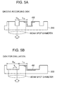
- the medium of the groove recording mode inevitably has a very narrow groove width. It is then difficult to increase the dimensional precision of the sample. It is then difficult to obtain data with a high reliability. Then, in order to obtain reliable data, the cross-erasing in the groove recording mode was measured by the following procedure using a disk for evaluation shown in FIG. 5B.
- FIG. 5A is a cross-sectional view for schematically illustrating a run made on a conventional groove recording disk by previously forming a recorded mark 4M in a track to be tested, and then irradiating a laser beam to an adjacent track to induce cross-erasing.
- FIG. 5B illustrates a medium 200 used in this Example.
- the land width Lw in FIG. 5B is equal to the land width Lw in FIG. 5A, whereas the groove width Gw in FIG. 5B is greater than the groove width Gw in FIG. 5A. Because of this design, the disk of FIG. 5B is easy to manufacture and has a high dimensional precision. In this state, the track pitch in FIG. 5B is greater than the track pitch in FIG. 5A.
- a recorded mark 4M is first formed in a track to be tested using a laser beam which is offset in the transverse (width) direction of the track, from which C1 is measured.
- the offset distance is set such that the distance of the recorded mark 4M extending over the land may be equal between FIGS. 5A and 5B, that is, the distance from the center of the land to the center of the beam spot may be equal between FIGS. 5A and 5B.
- a laser beam is irradiated to an adjacent track to induce cross-erasing.
- a laser beam which is offset in the transverse direction of the track is used as well.
- the offset distance To is equal to the offset distance used in the recorded mark formation.
- C2 is measured, from which C2-C1 is determined. It is understood that since this C2-C1 is the cross-erasing on one side of the recorded mark, similar measurement is made on the other side of the recorded mark. The sum of both the measurement results is the cross-erasing G-XE in the groove.
- Table 1 reports the track pitch P T used in each recording mode.
- the groove width was equal to the land width.
- the track pitch P T in the groove recording mode is an imaginary track pitch calculated from the offset of the laser beam and corresponds to Gw+Lw in FIG. 5A.
- an imaginary groove width Gw calculated from the offset of the laser beam that is, the value corresponding to Gw in FIG. 5A, was set so that the imaginary groove width divided by the imaginary track pitch, Gw/P T , might fall in the range between 0.30 and 0.35.
- Optical recording disk samples were fabricated as in Example 1 except that a supporting substrate 20 having a high dimensional precision in groove width was used and the track pitch P T was as shown in Table 2. It is noted that P T in Table 2 is not the imaginary track pitch in Example 1, but an actual track pitch.
- Example 2 These samples were evaluated as in Example 1. The results are shown in Table 2.
- a photomicrograph of the recording layer was taken through a transmission electron microscope. From the photomicrograph, the recorded mark width Mw was determined, and its ratio to groove width Gw and its ratio to track pitch P T were calculated. As a result, Mw/Gw was in the range between 2.0 and 2.8, and Mw/P T was in the range between 0.70 and 0.86.
- the light-transparent substrate 2 was formed by injection molding polycarbonate into a disk having a diameter of 120 mm and a thickness of 0.6 mm in which grooves were simultaneously formed.
- the track pitch P T was as shown in Table 3.
- the groove width Gw was set so that Gw/P T might fall in the range between 0.30 and 0.35.
- the groove width was equal to the land width.
- the first dielectric layer 31 was formed by sputtering a target of ZnS (80 mol%) and SiO 2 (20 mol%) in an Ar atmosphere.
- the first dielectric layer was 80 nm thick.
- the recording layer 4 was formed by sputtering an alloy target in an Ar atmosphere.
- the recording layer had the atomic ratio composition: (Sb 0.72 Te 0.28 ) 0.88 Ag 0.06 In 0.04 Ge 0.02 .
- the recording layer was 23 nm thick.
- the second dielectric layer 32 was formed by sputtering a target of ZnS (50 mol%) and SiO 2 (50 mol%) in an Ar atmosphere.
- the second dielectric layer was 25 nm thick.
- the ZnS-SiO 2 (50/50 mol%) used as the target had a thermal conductivity of 1.0 W/mK.
- the reflective layer 5 was formed as in Example 1.
- the protective layer 6 was formed by spin coating a UV-curable resin and irradiating UV thereto for curing.
- the protective layer was 5 ⁇ m thick.
- the disk sample thus fabricated was initialized or crystallized by means of a bulk eraser.
- the disk sample was determined for cross-erasing by the same procedure as in Example 1 and under the following conditions.
- the present invention employs the groove recording mode, succeeding in dramatically reducing the cross-erasing as compared with the land/groove recording mode. This enables to use a recording layer having a high crystallization speed which is otherwise difficult to reduce cross-erasing. Then a recording system with a high transfer rate is established. A possible reduction of the track pitch promises to establish a high-density recording system.
Landscapes
- Chemical & Material Sciences (AREA)
- Inorganic Chemistry (AREA)
- Optical Record Carriers And Manufacture Thereof (AREA)
- Thermal Transfer Or Thermal Recording In General (AREA)
- Optical Recording Or Reproduction (AREA)
Applications Claiming Priority (2)
| Application Number | Priority Date | Filing Date | Title |
|---|---|---|---|
| JP2000309956 | 2000-10-10 | ||
| JP2000309956 | 2000-10-10 |
Publications (2)
| Publication Number | Publication Date |
|---|---|
| EP1197955A2 true EP1197955A2 (de) | 2002-04-17 |
| EP1197955A3 EP1197955A3 (de) | 2006-11-22 |
Family
ID=18789998
Family Applications (1)
| Application Number | Title | Priority Date | Filing Date |
|---|---|---|---|
| EP01308615A Withdrawn EP1197955A3 (de) | 2000-10-10 | 2001-10-09 | Optisches Aufzeichnungsverfahren und -medium |
Country Status (5)
| Country | Link |
|---|---|
| US (1) | US7197005B2 (de) |
| EP (1) | EP1197955A3 (de) |
| KR (1) | KR100458299B1 (de) |
| CN (1) | CN1173337C (de) |
| TW (1) | TWI237244B (de) |
Cited By (3)
| Publication number | Priority date | Publication date | Assignee | Title |
|---|---|---|---|---|
| EP1688929A3 (de) * | 2004-11-30 | 2007-11-07 | TDK Corporation | Optisches Aufzeichnungsmedium und Testverfahren dafür |
| GB2457122A (en) * | 2008-01-31 | 2009-08-05 | Toshiba Kk | Recording medium amorphous mark with reduced recrystallization ring |
| EP2189980A1 (de) * | 2000-11-20 | 2010-05-26 | Sony Corporation | Optisches Aufzeichnungsmedium und optische Plattenvorrichtung |
Families Citing this family (7)
| Publication number | Priority date | Publication date | Assignee | Title |
|---|---|---|---|---|
| TWI244083B (en) * | 2001-07-18 | 2005-11-21 | Sony Corp | Optical recording/reproducing medium-use substrate, production method for optical recording/reproducing medium reproducing stamper and optical recording/reproducing medium producing stamper |
| KR20030030506A (ko) * | 2001-10-11 | 2003-04-18 | 삼성전자주식회사 | 고밀도 광디스크 |
| US7385907B2 (en) * | 2002-12-30 | 2008-06-10 | Koninklijke Philips Electronics N.V. | Rewritable optical record carrier |
| JP4484785B2 (ja) * | 2005-08-09 | 2010-06-16 | ソニー株式会社 | 記録方法 |
| US7835232B2 (en) * | 2006-06-27 | 2010-11-16 | International Business Machines Corporation | Method to erase data stored on blu-ray disc |
| JP2008033981A (ja) * | 2006-07-26 | 2008-02-14 | Tdk Corp | 光記録媒体の情報記録方法、光記録装置 |
| US10026443B1 (en) * | 2017-05-22 | 2018-07-17 | Seagate Technology Llc | Heat-assisted magnetic recording error-recovery by erasing adjacent tracks using laser |
Family Cites Families (22)
| Publication number | Priority date | Publication date | Assignee | Title |
|---|---|---|---|---|
| JPH05151619A (ja) * | 1991-10-01 | 1993-06-18 | Ricoh Co Ltd | 光情報記録媒体及び記録方法 |
| JP3413986B2 (ja) * | 1994-09-30 | 2003-06-09 | 三菱化学株式会社 | 光学的情報記録用媒体および記録再生方法 |
| US6167006A (en) * | 1995-03-31 | 2000-12-26 | Kabushiki Kaisha Toshiba | Optical information recording/reproducing apparatus based on tracking control of irradiated light |
| JPH09128827A (ja) * | 1995-08-29 | 1997-05-16 | Sony Corp | 光磁気記録媒体、記録方法及び光磁気記録装置 |
| JP3625541B2 (ja) * | 1995-09-13 | 2005-03-02 | 三菱化学株式会社 | 光記録媒体および記録再生方法 |
| EP0777216A3 (de) * | 1995-12-05 | 1998-12-23 | Nikon Corporation | Optische Platte mit hoher Speicherdichte, und Aufzeichnungsverfahren mit hoher Dichte |
| JPH10105968A (ja) * | 1996-09-24 | 1998-04-24 | Sony Corp | 光記録方法 |
| US6564009B2 (en) * | 1997-05-19 | 2003-05-13 | Sony Corporation | Apparatus for recording and/or reproducing data onto and/or from an optical disk and method thereof |
| JPH1166626A (ja) * | 1997-08-18 | 1999-03-09 | Sony Corp | 光ディスク及びその記録再生方法 |
| JPH1196579A (ja) * | 1997-09-19 | 1999-04-09 | Tdk Corp | 光記録媒体の記録再生方法および光記録媒体 |
| KR19990042064A (ko) * | 1997-11-25 | 1999-06-15 | 윤종용 | 귀금속 반사층을 구비한 상변화 광디스크 |
| CN1161766C (zh) * | 1998-02-24 | 2004-08-11 | 索尼株式会社 | 光记录介质 |
| JP3648378B2 (ja) * | 1998-03-20 | 2005-05-18 | 株式会社東芝 | 光ディスク |
| JP2000011453A (ja) | 1998-06-29 | 2000-01-14 | Sony Corp | 光記録媒体と光記録再生装置 |
| US6175548B1 (en) * | 1998-06-29 | 2001-01-16 | Sony Corporation | Optical recording medium and optical recording and reproducing apparatus |
| JP3502297B2 (ja) | 1998-07-21 | 2004-03-02 | Tdk株式会社 | 光記録方法 |
| WO2000021081A1 (en) * | 1998-10-07 | 2000-04-13 | Hitachi, Ltd. | Information recording medium and information recording device |
| JP2000123416A (ja) | 1998-10-14 | 2000-04-28 | Sony Corp | 光記録媒体と光記録再生装置 |
| US6449239B1 (en) * | 1998-11-25 | 2002-09-10 | Matsushita Electric Industrial Co., Ltd. | Optical information recording medium with thermal diffusion layer |
| KR100561382B1 (ko) * | 1999-03-25 | 2006-03-16 | 삼성전자주식회사 | 광디스크 기판 |
| JP2001229546A (ja) * | 2000-02-14 | 2001-08-24 | Sony Corp | 光記録媒体及び光記録媒体製造用原盤 |
| JP4233224B2 (ja) * | 2000-02-21 | 2009-03-04 | Tdk株式会社 | 光記録媒体 |
-
2001
- 2001-10-06 KR KR10-2001-0061615A patent/KR100458299B1/ko not_active Expired - Lifetime
- 2001-10-08 TW TW090124861A patent/TWI237244B/zh not_active IP Right Cessation
- 2001-10-09 EP EP01308615A patent/EP1197955A3/de not_active Withdrawn
- 2001-10-09 US US09/971,704 patent/US7197005B2/en not_active Expired - Lifetime
- 2001-10-10 CN CNB011412305A patent/CN1173337C/zh not_active Expired - Lifetime
Non-Patent Citations (2)
| Title |
|---|
| NARAHARA T ET AL: "OPTICAL DISC SYSTEM FOR DIGITAL VIDEO RECORDING", JAPANESE JOURNAL OF APPLIED PHYSICS, JAPAN SOCIETY OF APPLIED PHYSICS, JP, vol. 39, no. 2B, PART 01, 11 July 1999 (1999-07-11), pages 912 - 919, XP001005912, ISSN: 0021-4922, DOI: 10.1143/JJAP.39.912 * |
| YUTAKA KASAMI: "Large Capacity and High-Data-Rate Phase-Change Disks", JAPANESE JOURNAL OF APPLIED PHYSICS, JAPAN SOCIETY OF APPLIED PHYSICS, JP, vol. 39, no. 2B, 1 February 2000 (2000-02-01), pages 756 - 761, XP002427178, ISSN: 0021-4922, DOI: 10.1143/JJAP.39.756 * |
Cited By (4)
| Publication number | Priority date | Publication date | Assignee | Title |
|---|---|---|---|---|
| EP2189980A1 (de) * | 2000-11-20 | 2010-05-26 | Sony Corporation | Optisches Aufzeichnungsmedium und optische Plattenvorrichtung |
| EP1688929A3 (de) * | 2004-11-30 | 2007-11-07 | TDK Corporation | Optisches Aufzeichnungsmedium und Testverfahren dafür |
| US7580340B2 (en) | 2004-11-30 | 2009-08-25 | Tdk Corporation | Optical recording medium and a method for testing the same |
| GB2457122A (en) * | 2008-01-31 | 2009-08-05 | Toshiba Kk | Recording medium amorphous mark with reduced recrystallization ring |
Also Published As
| Publication number | Publication date |
|---|---|
| TWI237244B (en) | 2005-08-01 |
| US20020064122A1 (en) | 2002-05-30 |
| US7197005B2 (en) | 2007-03-27 |
| CN1173337C (zh) | 2004-10-27 |
| KR20020028795A (ko) | 2002-04-17 |
| KR100458299B1 (ko) | 2004-11-26 |
| EP1197955A3 (de) | 2006-11-22 |
| CN1365101A (zh) | 2002-08-21 |
Similar Documents
| Publication | Publication Date | Title |
|---|---|---|
| US6040030A (en) | Optical recording medium | |
| US6798733B2 (en) | Optical recording method and medium | |
| US6656559B2 (en) | Optical recording medium and optical recording method therefor | |
| US6329036B1 (en) | Optical recording medium and use | |
| US5627012A (en) | Method for preparing phase change optical recording medium | |
| US5523140A (en) | Optical recording method and medium | |
| EP1213715A2 (de) | Optisches Aufzeichnungsmedium | |
| US6461710B1 (en) | Optical recording medium | |
| EP1030292B1 (de) | Optischer Aufzeichnungsträger und Verfahren zu dessen Initialisierung | |
| US5906874A (en) | Optical recording medium, and its fabrication method | |
| US5978349A (en) | Optical recording medium | |
| US7197005B2 (en) | Optical recording method and medium | |
| EP1102252A2 (de) | Optisches Phasenwechselaufzeichnungsmedium mit Kristallkeimbildungsschicht | |
| US6071587A (en) | Optical recording medium and its recording method | |
| US6042921A (en) | Optical recording medium and read/write method therefor | |
| EP1447795A1 (de) | Optisches aufzeichnungsmedium | |
| EP1143427A2 (de) | Optisches Aufzeichnungsverfahren, optisches Aufzeichnungsgerät und optisches Aufzeichnungsmedium | |
| US20040213121A1 (en) | Optical recording medium and optical recording method | |
| US6192024B1 (en) | Optical recording medium | |
| US6618349B2 (en) | Optical recording medium and its designing method | |
| US20050221049A1 (en) | Optical recording medium | |
| EP1011099B1 (de) | Optisches Aufzeichnungsverfahren | |
| WO2002043060A1 (fr) | Moyen d'enregistrement optique | |
| US6403193B1 (en) | Optical recording medium | |
| US6733858B2 (en) | Optical recording medium and optical recording method therefor |
Legal Events
| Date | Code | Title | Description |
|---|---|---|---|
| PUAI | Public reference made under article 153(3) epc to a published international application that has entered the european phase |
Free format text: ORIGINAL CODE: 0009012 |
|
| AK | Designated contracting states |
Kind code of ref document: A2 Designated state(s): AT BE CH CY DE DK ES FI FR GB GR IE IT LI LU MC NL PT SE TR |
|
| AX | Request for extension of the european patent |
Free format text: AL;LT;LV;MK;RO;SI |
|
| PUAL | Search report despatched |
Free format text: ORIGINAL CODE: 0009013 |
|
| AK | Designated contracting states |
Kind code of ref document: A3 Designated state(s): AT BE CH CY DE DK ES FI FR GB GR IE IT LI LU MC NL PT SE TR |
|
| AX | Request for extension of the european patent |
Extension state: AL LT LV MK RO SI |
|
| 17P | Request for examination filed |
Effective date: 20070404 |
|
| AKX | Designation fees paid |
Designated state(s): DE FR GB |
|
| 17Q | First examination report despatched |
Effective date: 20070710 |
|
| STAA | Information on the status of an ep patent application or granted ep patent |
Free format text: STATUS: THE APPLICATION IS DEEMED TO BE WITHDRAWN |
|
| 18D | Application deemed to be withdrawn |
Effective date: 20110524 |