EP1198162A2 - Element mit montiertem elektronischem Bauteil und Verfahren zu dessen Reparatur - Google Patents
Element mit montiertem elektronischem Bauteil und Verfahren zu dessen Reparatur Download PDFInfo
- Publication number
- EP1198162A2 EP1198162A2 EP01115885A EP01115885A EP1198162A2 EP 1198162 A2 EP1198162 A2 EP 1198162A2 EP 01115885 A EP01115885 A EP 01115885A EP 01115885 A EP01115885 A EP 01115885A EP 1198162 A2 EP1198162 A2 EP 1198162A2
- Authority
- EP
- European Patent Office
- Prior art keywords
- electrically conductive
- electronic component
- circuit board
- intermediate layer
- mounted member
- Prior art date
- Legal status (The legal status is an assumption and is not a legal conclusion. Google has not performed a legal analysis and makes no representation as to the accuracy of the status listed.)
- Withdrawn
Links
Images


Classifications
-
- H—ELECTRICITY
- H05—ELECTRIC TECHNIQUES NOT OTHERWISE PROVIDED FOR
- H05K—PRINTED CIRCUITS; CASINGS OR CONSTRUCTIONAL DETAILS OF ELECTRIC APPARATUS; MANUFACTURE OF ASSEMBLAGES OF ELECTRICAL COMPONENTS
- H05K3/00—Apparatus or processes for manufacturing printed circuits
- H05K3/30—Assembling printed circuits with electric components, e.g. with resistors
- H05K3/32—Assembling printed circuits with electric components, e.g. with resistors electrically connecting electric components or wires to printed circuits
- H05K3/321—Assembling printed circuits with electric components, e.g. with resistors electrically connecting electric components or wires to printed circuits by conductive adhesives
-
- H—ELECTRICITY
- H05—ELECTRIC TECHNIQUES NOT OTHERWISE PROVIDED FOR
- H05K—PRINTED CIRCUITS; CASINGS OR CONSTRUCTIONAL DETAILS OF ELECTRIC APPARATUS; MANUFACTURE OF ASSEMBLAGES OF ELECTRICAL COMPONENTS
- H05K2201/00—Indexing scheme relating to printed circuits covered by H05K1/00
- H05K2201/01—Dielectrics
- H05K2201/0104—Properties and characteristics in general
- H05K2201/0129—Thermoplastic polymer, e.g. auto-adhesive layer; Shaping of thermoplastic polymer
-
- H—ELECTRICITY
- H05—ELECTRIC TECHNIQUES NOT OTHERWISE PROVIDED FOR
- H05K—PRINTED CIRCUITS; CASINGS OR CONSTRUCTIONAL DETAILS OF ELECTRIC APPARATUS; MANUFACTURE OF ASSEMBLAGES OF ELECTRICAL COMPONENTS
- H05K2201/00—Indexing scheme relating to printed circuits covered by H05K1/00
- H05K2201/10—Details of components or other objects attached to or integrated in a printed circuit board
- H05K2201/10613—Details of electrical connections of non-printed components, e.g. special leads
- H05K2201/10954—Other details of electrical connections
- H05K2201/10992—Using different connection materials, e.g. different solders, for the same connection
-
- H—ELECTRICITY
- H05—ELECTRIC TECHNIQUES NOT OTHERWISE PROVIDED FOR
- H05K—PRINTED CIRCUITS; CASINGS OR CONSTRUCTIONAL DETAILS OF ELECTRIC APPARATUS; MANUFACTURE OF ASSEMBLAGES OF ELECTRICAL COMPONENTS
- H05K2203/00—Indexing scheme relating to apparatus or processes for manufacturing printed circuits covered by H05K3/00
- H05K2203/17—Post-manufacturing processes
- H05K2203/176—Removing, replacing or disconnecting component; Easily removable component
-
- H—ELECTRICITY
- H05—ELECTRIC TECHNIQUES NOT OTHERWISE PROVIDED FOR
- H05K—PRINTED CIRCUITS; CASINGS OR CONSTRUCTIONAL DETAILS OF ELECTRIC APPARATUS; MANUFACTURE OF ASSEMBLAGES OF ELECTRICAL COMPONENTS
- H05K2203/00—Indexing scheme relating to apparatus or processes for manufacturing printed circuits covered by H05K3/00
- H05K2203/30—Details of processes not otherwise provided for in H05K2203/01 - H05K2203/17
- H05K2203/306—Lifting the component during or after mounting; Increasing the gap between component and PCB
-
- Y—GENERAL TAGGING OF NEW TECHNOLOGICAL DEVELOPMENTS; GENERAL TAGGING OF CROSS-SECTIONAL TECHNOLOGIES SPANNING OVER SEVERAL SECTIONS OF THE IPC; TECHNICAL SUBJECTS COVERED BY FORMER USPC CROSS-REFERENCE ART COLLECTIONS [XRACs] AND DIGESTS
- Y10—TECHNICAL SUBJECTS COVERED BY FORMER USPC
- Y10T—TECHNICAL SUBJECTS COVERED BY FORMER US CLASSIFICATION
- Y10T29/00—Metal working
- Y10T29/49—Method of mechanical manufacture
- Y10T29/49002—Electrical device making
- Y10T29/49117—Conductor or circuit manufacturing
- Y10T29/49169—Assembling electrical component directly to terminal or elongated conductor
- Y10T29/49171—Assembling electrical component directly to terminal or elongated conductor with encapsulating
- Y10T29/49172—Assembling electrical component directly to terminal or elongated conductor with encapsulating by molding of insulating material
Definitions
- the present invention relates to an electronic component mounted member in which an electronic component and a circuit board are joined via an electrically conductive adhesive, in the field of mounting electronic components, and to an electronic component mounted member and a repair method thereof permitting improved repair of the component.
- the conventional electrically conductive adhesive is formed by dispersing an electrically conductive filler into a resin-based adhesive component. After a terminal of an electronic component and that of a circuit board are connected via the electrically conductive adhesive, the resin is cured, thereby maintaining a conduction of the connected portions by a contact of the electrically conductive fillers.
- the electrically conductive adhesive is expected as an alternative material to the solder.
- thermosetting epoxy binder resin often is used for a binder resin of the electrically conductive adhesive.
- the electrically conductive adhesive remains on a substrate electrode.
- the substrate electrode is peeled off from a substrate base material, or neighboring components are damaged.
- thermoplastic binder resins are just becoming commercially-available as an electrically conductive adhesive that is capable of repair.
- electrically conductive adhesives do not have a sufficient connection strength, and are, therefore, insufficient for a material for mounting electronic components.
- a mixture of the thermoplastic binder resin and the thermosetting binder resin has a better connection strength than the electrically conductive adhesive of the thermoplastic binder resin alone, the binder resin forms a lump and remains on a surface of the substrate electrode, so that, after the removal of the electronic component, a mounting work of a replacement electronic component becomes complicated.
- a first electronic component mounted member of the present invention includes a circuit board, an electronic component connected to the circuit board, and an electrically conductive adhesive interposed between the electronic component and the circuit board.
- an intermediate layer that is formed of a thermoplastic insulating adhesive with a softening temperature of 100°C to 300°C is interposed between the electrically conductive adhesive and the electrode.
- An electrically conductive filler contained in the electrically conductive adhesive is present partially in the intermediate layer, thus allowing an electrical conduction between the electrically conductive adhesive and the electrode of the circuit board.
- a second electronic component mounted member of the present invention includes a circuit board, an electronic component connected to the circuit board, and an electrically conductive adhesive interposed between the electronic component and the circuit board.
- an intermediate layer that is formed of a thermoplastic insulating adhesive with a softening temperature of 100°C to 300°C and contains an electrically conductive expandable particle is interposed between the electrically conductive adhesive and the electrode.
- the electrically conductive expandable particle allows an electrical conduction between the electrically conductive adhesive and the electrode of the circuit board.
- a repair method of an electronic component mounted member of the present invention includes using the mounted member including a circuit board and an electronic component connected to the circuit board, and when a repair is necessary, heating a portion of the intermediate layer corresponding to the electronic component to be repaired so as to raise a temperature of this portion to at least a melting point of the thermoplastic insulating adhesive, thereby melting the thermoplastic insulating adhesive, and removing the electronic component with this state maintained.
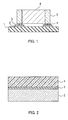
- FIG. 1 shows a cross-section of an electronic component mounted member according to an example of the present invention.
- FIG. 2 shows a cross-section of a connected portion of an electronic component mounted member in which an acrylic resin is used for an intermediate layer according to Example 1 of the present invention.
- FIG. 3 shows a cross-section of a connected portion of an electronic component mounted member in which an acrylic resin is used for an intermediate layer and an adhesion of an electronic component is reinforced by an insulating adhesive according to Example 2 of the present invention.
- FIG. 4 shows a cross-section of a connected portion of an electronic component mounted member in which an acrylic resin layer containing a gold-plated expandable particle is used for an intermediate layer according to Example 3 of the present invention.
- FIG. 5 shows a cross-section of the electronic component mounted member according to Example 3.
- FIG. 6A shows a schematic cross-section for describing an electrical connection more specifically in an example of the present invention
- FIG. 6B shows a schematic cross-section of the enlarged electrically connected portion in FIG. 6A.
- the present invention is directed to an electronic component mounted member and a repair method thereof, in which an intermediate layer formed of an insulating adhesive with a specific softening temperature ranging from 100°C to 300°C is formed between an electrically conductive adhesive and an electrode of a circuit board.
- the intermediate layer with a specific softening temperature is interposed between the electrically conductive adhesive and the circuit board electrode
- spot-heating heating only a portion that needs repairing
- the intermediate layer melts. Then, with this state maintained, the electronic component can be grasped and removed easily.
- the area where the intermediate layer is formed is not smaller than that where the electrically conductive adhesive is formed. Furthermore, it is preferable that the area where the intermediate layer is formed is one to two times as large as that the electrically conductive adhesive is formed. It is particularly preferable that the former is 1.1 times to 1.5 times as large as the latter.
- the intermediate layer of the present invention has a thickness of 0.05 ⁇ m to 10 ⁇ m.
- the intermediate layer is broken partially by a pressure of an electrically conductive metal filler contained in the electrically conductive adhesive, thus allowing an electrical conduction between the electrically conductive adhesive and the circuit board electrode.
- the intermediate layer is thinner than 0.05 ⁇ m, it may be difficult to form the intermediate layer on the entire surface of the connected portion uniformly.
- it is thicker than 10 ⁇ m, a material cost and a process cost in terms of a formation time tend to increase.
- the intermediate layer may become difficult to be broken, leading to a poor electrical conduction between the electrically conductive adhesive and the circuit board electrode.
- the electrically conductive adhesive is formed again, and an alternative electronic component is mounted, followed by curing the electrically conductive adhesive. In this manner, it becomes possible to obtain an excellent electronic component mounted member.
- thermoplastic insulating adhesive with a specific softening temperature of the present invention is a substance having a melting point that is higher than a curing temperature of the electrically conductive adhesive and does not easily damage the circuit board and electronic components mounted on the periphery of the electronic component to be repaired.
- the thermoplastic insulating adhesive may be thermoplastic epoxy resin, acrylic resin or vinyl resin.
- the softening temperature of polymers is slightly (more specifically, a few degrees) lower than their melting point, the softening temperature substantially can be regarded as the melting point.
- an electrically conductive expandable particle that expands at a specific temperature may be mixed in the insulating adhesive.
- the insulating adhesive mixed with the electrically conductive expandable particle expands when it is heated to the temperature equal to or higher than an expansion temperature of this expandable particle.
- the electronic component mounted member of the present invention obtained by interposing such insulating adhesive layer between the electrically conductive adhesive and the circuit board electrode is heated to maintain the expansion temperature, the insulating adhesive layer expands, making a repair easier.
- the electrically conductive expandable particle is a substance having a preferable expansion temperature that is higher than the curing temperature of the electrically conductive adhesive and the softening temperature of the cured electrically conductive adhesive and low enough not to easily damage components other than the component to be repaired or the circuit board.
- the content of the electrically conductive expandable particle preferably is from 2 vol% to 50 vol%, and more preferably is from 5 vol% to 20 vol%. The content less than 2 vol% may not lead to a notable effect of adding the electrically conductive expandable particle, while that more than 50 vol% may bring about a lower connection strength, which is not preferable in practice.
- the electrically conductive expandable particle has a mean particle diameter of 1 ⁇ m to 10 ⁇ m.
- the electrically conductive expandable particle may be an expandable resin whose surface is coated with metal such as gold, and therefore is electrically conductive in itself.
- the intermediate layer has a thickness that does not have a harmful effect on the electrical connection by the electrically conductive adhesive between the electronic component and the circuit board electrode in practice.
- the thickness of the intermediate layer is, for example, approximately the same or less than the size of the electrically conductive filler contained in the electrically conductive adhesive.
- the intermediate layer has a thickness of 0.05 ⁇ m to 10 ⁇ m. If the intermediate layer is thinner than 0.05 ⁇ m, a binder resin component of the electrically conductive adhesive may adhere directly to the circuit board electrode, making it difficult to achieve an excellent repair. On the other hand, if it is thicker than 10 ⁇ m, it may become difficult to maintain a good contact between the electrically conductive filler and the circuit board electrode, increasing the connection resistance.
- FIG. 1 shows a schematic structure of an electronic component mounted member in which electrodes 5 of an electronic component 6 and electrodes 2 of a circuit board 1 are connected to each other via electrically conductive adhesives 4 and intermediate layers (insulating adhesive resin) 3.
- electrically conductive adhesives 4 and intermediate layers (insulating adhesive resin) 3 When the area where the electrically conductive adhesive 4 is formed is larger than that where the intermediate layer (insulating adhesive) 3 is formed so that the electrically conductive adhesive 4 directly contacts the circuit board 1 or the electrode 2, the effect of the intermediate layer (insulating adhesive resin layer) 3 is not fully expressed because of poor repair characteristics of the electrically conductive adhesive 4.
- a binder resin component of the electrically conductive adhesive 4 remains on the circuit board 1 or the electrode 2.
- the formed area of the electrically conductive adhesive 4 and that of the intermediate layer (the insulating adhesive resin) 3 achieve the above relationship.
- a chip resistor 6 having terminal electrodes 5 is electrically connected onto the electrodes 2 of the circuit board 1 provided with the intermediate layers 3 of an electrically conductive medium preferable for a repair of the present invention via the electrically conductive adhesives 4.
- FIGs. 6A and 6B show schematic cross-sections for more specifically describing the electrical connection mentioned above.
- the electrically conductive adhesive 4 and the intermediate layer (the insulating adhesive resin) 3 are interposed and connected between the electrode 2 formed on the surface of the circuit board and the electrode (not shown in this figure) of the electronic component, so as to form the mounted member.
- the electrically connected portion of FIG. 6A is enlarged and shown in FIG. 6B.
- An electrically conductive filler 7 in the electrically conductive adhesive 4 penetrates the intermediate layer 3 so as to contact the substrate electrode 2, thus conducting electricity. This process is explained as follows. After forming the intermediate layer 3 on the surface of the substrate electrode 2, the electrically conductive adhesive 4 is formed by printing.
- the electrically conductive adhesive 4 also is pressed by a mounter, so that the electrically conductive filler 7 in the electrically conductive adhesive 4 cuts into the intermediate layer 3.
- the substrate electrode 2 and the electrically conductive filler 7 contact each other.
- the relationship between the thickness of the intermediate layer and the diameter of the electrically conductive filler is selected appropriately.
- the above-described insulating adhesive resin with a specific softening temperature may be formed on the surface of the electrode of the circuit board and/or the surface of the circuit board.
- the circuit board with such a structure is appropriate for realizing the repair method of the present invention mentioned above.
- the electronic component mounted member of the present invention it is possible to solve the conventional problem of repairing in the mounting technique of the electronic components using the electrically conductive adhesive and achieve a repair of substantially the same degree as that of the conventional soldering connection without using such solder connection.
- the intermediate layer with a specific softening point is formed on a joining interface of the electronic component and the circuit board, thus making it possible to improve repair characteristics of the electronic components practically, which conventionally have been a problem in the connection with the electrically conductive adhesive.
- the present invention can achieve an electronic component and an electronic component mounted member using no lead. This also is appropriate for responding to environmental issues, which have attracted wide attention recently.
- the chip resistor In a condition where a warm air jet with a temperature of 220°C is blown against the chip resistor 6 from 5 cm above it, the chip resistor is clamped by a pincher-shaped jig that is directly connected to a load cell and raised vertically upward so as to observe and evaluate the strength of the chip resistor at the time of its removal and a surface condition of the substrate electrode when the chip resistor is removed successfully.
- FIG. 2 shows a schematic cross-section of a connected portion when the chip resistor (not shown in this figure) was connected to the circuit board using the electrically conductive adhesive 4 in the above-described basic structure of the present invention shown in FIG. 1.
- the intermediate layer 3 of a thermoplastic insulating adhesive with a softening point of 150°C was formed on the surface of the electrode 2 of the circuit board.
- the intermediate layer 3 was formed by spray coating a solution in which acrylic resin (acrylic adhesive, manufactured by Toyobo Co., Ltd.) was dissolved in an alcoholic solvent (ethanol) in the resin-ethanol ratio of 10wt% : 90wt%.
- the thickness after drying is shown in Table 1.
- the formed area of the intermediate layer was 7.6 mm 2 (2.0 mm ⁇ 3.8 mm), and that of the electrically conductive adhesive was 6.12 mm 2 (1.8 mm ⁇ 3.4 mm).
- thermosetting epoxy resin-based electrically conductive adhesive containing 80 vol% of mercury as a electrically conductive filler was used as the electrically conductive adhesive 4.
- a glass epoxy substrate was used as the base material of the circuit board.
- the prepared chip resistor was mounted on the circuit board 1 using the electrically conductive adhesive 4 and cured in an oven at 150°C for one hour.
- Such electronic component mounted members were produced with various specifications of the intermediate layers 3, and their repair characteristics were evaluated.
- the surface of the electrode 2 of the circuit board and the surface of the circuit board 1 first were plated with solder having a thickness of 0.5 ⁇ m, and then an intermediate layer 8 further was formed thereon by spray coating an alcoholic solvent containing the same acrylic resin (softening point: 150°C) as that in Example 1 as a binder component, so as to obtain a thickness after drying of 0.5 ⁇ m.
- the formed area of the intermediate layer 8 was 7.6 mm 2 (2.0 mm ⁇ 3.8 mm), and that of the electrically conductive adhesive was 6.12 mm 2 (1.8 mm ⁇ 3.4 mm).
- the chip resistor 6 was connected to the circuit board using the electrically conductive adhesive 4 and an electrically insulating adhesive 9 for reinforcement.
- the electrically conductive adhesive had the effects of an electrical connection and an adhesion, while the insulating adhesive 9 had the effect of reinforcing the adhesion.
- An epoxy adhesive (Amicon C-990J #330, manufactured by EMERSON & CUMING Inc.) was used as the electrically insulating adhesive 9.
- the electrically conductive adhesive 4 used in this example was the same as that in Example 1. As shown in FIG. 3, the prepared chip resistor 6 was mounted on the circuit board 1 using the electrically conductive adhesive 4 and cured in an oven at 150°C for one hour. The repair characteristics of this electronic component mounted member were evaluated.
- the intermediate layer 3 was formed by solder plating to obtain a thickness of 0.5 ⁇ m, so as to achieve the relationship of the formed area of the intermediate layer ⁇ that of the electrically conductive adhesive.
- the formed area of the intermediate layer was 7.6 mm 2 (2.0 mm ⁇ 3.8 mm), and that of the electrically conductive adhesive was 9.66 mm 2 (2.3 mm ⁇ 4.2 mm).
- the results are shown in Table 2.
- FIG. 4 shows a schematic cross-section of a connected portion when the chip resistor was connected to the circuit board using the electrically conductive adhesive 4 in the above-described basic structure of the present invention shown in FIG. 1.
- the surface of an expandable particle called F-80VS manufactured by MATSUMOTO YUSHI-SEIYAKU Co., Ltd., (whose particle diameter is 6 ⁇ m to 10 ⁇ m) was plated with gold having a thickness of about 0.05 ⁇ m by an electroless deposition so as to be provided with an electrical conductivity.
- thermoplastic insulating adhesive with a specific melting point containing the electrically conductive expandable particle was formed on the surface of the electrode 2 of the circuit board by spray coating a solution in which the same acrylic resin as in Example 1 (solid blending quantity: 10wt%) containing the above filler (blending quantity: 15 vol%) was dissolved in an alcoholic solvent.
- the electrically conductive adhesive 4 used in this example was the same as that in Example 1. As shown in FIG. 5, the prepared chip resistor 6 was mounted on the circuit board 1 using the electrically conductive adhesive 4 and cured in an oven at 150°C for one hour. The repair characteristics of this electronic component mounted member were evaluated.
- Example 3 the intermediate layer 3 of Example 1 was used for comparison.
- connection resistance of evaluated samples in addition to the items evaluated in Example 1, was measured, which indicated an effect of reducing the connection resistance expected in the present invention.
- the results of these measurements are shown in Table 3.
- Intermediate layer specification Surface condition after component removal Component removal load (N) Connection resistance before repairing (m ⁇ ) Adhesive residue Electrode damage (Example 3) Acrylic resin 5 ⁇ m + expandable particle None None 8.9 12.3 (Reference example 3) Acrylic resin 5 ⁇ m None None 8.5 35.1
- the electronic component was the chip resistor. However, it is not limited to the above as long as it is a commonly-used electronic component such as a semiconductor package and a connector.
- the intermediate layer was formed on the surface of the circuit board electrode in the above examples, it may be formed on the surface of the electronic component in the present invention. Also, the intermediate layer may be formed on the surface of an anisotropic conductive film (ACF) so as to be used for the connection of the electronic component.
- ACF anisotropic conductive film
- the intermediate layer with a specific melting point is formed on a joining interface of the electronic component and the circuit board, thus making it possible to improve repair characteristics of the electronic components practically, which conventionally have been a problem in the connection with the electrically conductive adhesive.
- the present invention can achieve the electronic component and the electronic component mounted member using no lead. This also is appropriate for responding to environmental issues, which have attracted wide attention recently.
Landscapes
- Engineering & Computer Science (AREA)
- Manufacturing & Machinery (AREA)
- Microelectronics & Electronic Packaging (AREA)
- Electric Connection Of Electric Components To Printed Circuits (AREA)
- Structures For Mounting Electric Components On Printed Circuit Boards (AREA)
Applications Claiming Priority (2)
| Application Number | Priority Date | Filing Date | Title |
|---|---|---|---|
| JP2000309693 | 2000-10-10 | ||
| JP2000309693 | 2000-10-10 |
Publications (2)
| Publication Number | Publication Date |
|---|---|
| EP1198162A2 true EP1198162A2 (de) | 2002-04-17 |
| EP1198162A3 EP1198162A3 (de) | 2004-01-21 |
Family
ID=18789805
Family Applications (1)
| Application Number | Title | Priority Date | Filing Date |
|---|---|---|---|
| EP01115885A Withdrawn EP1198162A3 (de) | 2000-10-10 | 2001-06-29 | Element mit montiertem elektronischem Bauteil und Verfahren zu dessen Reparatur |
Country Status (2)
| Country | Link |
|---|---|
| US (2) | US6512183B2 (de) |
| EP (1) | EP1198162A3 (de) |
Cited By (1)
| Publication number | Priority date | Publication date | Assignee | Title |
|---|---|---|---|---|
| EP2621254A1 (de) * | 2012-01-25 | 2013-07-31 | In2Tec Limited | Recycelbare Schaltungsanordnung |
Families Citing this family (18)
| Publication number | Priority date | Publication date | Assignee | Title |
|---|---|---|---|---|
| US7161252B2 (en) * | 2002-07-19 | 2007-01-09 | Matsushita Electric Industrial Co., Ltd. | Module component |
| JP3755824B2 (ja) * | 2003-03-04 | 2006-03-15 | 株式会社らいふ | 複数電極接着用の電子部品とその実装方法 |
| JP2005026525A (ja) * | 2003-07-03 | 2005-01-27 | Shinko Electric Ind Co Ltd | 配線基板および配線基板の製造方法 |
| US6790051B1 (en) * | 2003-12-20 | 2004-09-14 | Lear Corporation | Connector for printed circuit board |
| TWI230995B (en) * | 2004-05-28 | 2005-04-11 | Via Tech Inc | Electronic package with passive components |
| US7459795B2 (en) * | 2004-08-19 | 2008-12-02 | Formfactor, Inc. | Method to build a wirebond probe card in a many at a time fashion |
| US7170187B2 (en) * | 2004-08-31 | 2007-01-30 | International Business Machines Corporation | Low stress conductive polymer bump |
| CA2490676A1 (en) * | 2004-12-16 | 2006-06-16 | Ibm Canada Limited - Ibm Canada Limitee | Releasably mountable electronics component |
| TWI348341B (en) * | 2005-05-18 | 2011-09-01 | Chunghwa Picture Tubes Ltd | Electronic element module and electronic device using the same |
| US7700901B2 (en) * | 2006-02-10 | 2010-04-20 | Radiant Glass Industries, Llc | Heated glass panels |
| US7362491B2 (en) * | 2006-02-10 | 2008-04-22 | Radiant Glass Industries, Llc | Heated glass panels and methods for making electrical contact with electro-conductive films |
| US7836587B2 (en) | 2006-09-21 | 2010-11-23 | Formfactor, Inc. | Method of repairing a contactor apparatus |
| JP4865067B1 (ja) * | 2010-07-30 | 2012-02-01 | 株式会社東芝 | 電子機器 |
| JP5644286B2 (ja) * | 2010-09-07 | 2014-12-24 | オムロン株式会社 | 電子部品の表面実装方法及び電子部品が実装された基板 |
| JP5647335B2 (ja) | 2011-03-29 | 2014-12-24 | パナソニックIpマネジメント株式会社 | はんだ転写基材、はんだ転写基材の製造方法、及びはんだ転写方法 |
| KR101963273B1 (ko) * | 2014-09-18 | 2019-03-28 | 삼성전기주식회사 | 인터포저, 인터포저를 포함하는 전자 부품 및 인터포저를 포함하는 전자 부품의 실장 기판 |
| TWI696300B (zh) | 2016-03-15 | 2020-06-11 | 晶元光電股份有限公司 | 半導體裝置及其製造方法 |
| US10388464B2 (en) * | 2016-09-19 | 2019-08-20 | Biotronik Se & Co. Kg | Method for manufacturing a leadless solid electrolyte capacitor and corresponding capacitor |
Family Cites Families (33)
| Publication number | Priority date | Publication date | Assignee | Title |
|---|---|---|---|---|
| US4885126A (en) * | 1986-10-17 | 1989-12-05 | Polonio John D | Interconnection mechanisms for electronic components |
| EP0360971A3 (de) * | 1988-08-31 | 1991-07-17 | Mitsui Mining & Smelting Co., Ltd. | Substrat für die Montage und sein Herstellungsverfahren und gedruckte Leiterplatte mit Verbinderfunktion und Verbindungsverfahren hierfür |
| JPH02182050A (ja) | 1989-01-06 | 1990-07-16 | Nec Corp | 複合ローカルエリアネットワークシステム |
| US5291371A (en) * | 1990-04-27 | 1994-03-01 | International Business Machines Corporation | Thermal joint |
| JPH0710030B2 (ja) * | 1990-05-18 | 1995-02-01 | インターナシヨナル・ビジネス・マシーンズ・コーポレーシヨン | 多層配線基板の製造方法 |
| JPH04267586A (ja) * | 1991-02-22 | 1992-09-24 | Nec Corp | 同軸配線パターンおよびその形成方法 |
| JPH0574857A (ja) | 1991-09-11 | 1993-03-26 | Hitachi Ltd | 半導体装置 |
| EP0547807A3 (en) * | 1991-12-16 | 1993-09-22 | General Electric Company | Packaged electronic system |
| JPH05275489A (ja) | 1992-03-26 | 1993-10-22 | Hitachi Ltd | 電極間の接続構造 |
| US5255431A (en) * | 1992-06-26 | 1993-10-26 | General Electric Company | Method of using frozen epoxy for placing pin-mounted components in a circuit module |
| US5324888A (en) * | 1992-10-13 | 1994-06-28 | Olin Corporation | Metal electronic package with reduced seal width |
| US5657075A (en) * | 1993-02-05 | 1997-08-12 | Teradyne, Inc. | Method and apparatus for locating and facilitating the repair of defects on a printed circuit board |
| DE69426347T2 (de) * | 1993-09-29 | 2001-05-17 | Matsushita Electric Industrial Co., Ltd. | Verfahren zum Montieren einer Halbleiteranordnung auf einer Schaltungsplatte und eine Schaltungsplatte mit einer Halbleiteranordnung darauf |
| US5579573A (en) * | 1994-10-11 | 1996-12-03 | Ford Motor Company | Method for fabricating an undercoated chip electrically interconnected to a substrate |
| CN1194059A (zh) * | 1995-08-29 | 1998-09-23 | 美国3M公司 | 用于粘合电子器件的可变形基片部件 |
| JPH09148720A (ja) | 1995-11-27 | 1997-06-06 | Toshiba Corp | マルチチップモジュールの製造方法 |
| JP3111010B2 (ja) | 1996-01-24 | 2000-11-20 | インターナショナル・ビジネス・マシーンズ・コーポレ−ション | 導電性ペースト |
| US5761048A (en) * | 1996-04-16 | 1998-06-02 | Lsi Logic Corp. | Conductive polymer ball attachment for grid array semiconductor packages |
| US5809641A (en) * | 1996-04-25 | 1998-09-22 | International Business Machines Corporation | Method for printed circuit board repair |
| JP3687041B2 (ja) * | 1997-04-16 | 2005-08-24 | 大日本印刷株式会社 | 配線基板、配線基板の製造方法、および半導体パッケージ |
| US6297559B1 (en) * | 1997-07-10 | 2001-10-02 | International Business Machines Corporation | Structure, materials, and applications of ball grid array interconnections |
| JPH1135904A (ja) * | 1997-07-17 | 1999-02-09 | Alps Electric Co Ltd | 導電性組成物およびそれを用いた電子機器 |
| CA2310765C (en) | 1997-11-19 | 2005-07-12 | Hiroaki Takezawa | Stress relaxation type electronic component, a stress relaxation type circuit board, and a stress relaxation type electronic component mounted member |
| US5888884A (en) * | 1998-01-02 | 1999-03-30 | General Electric Company | Electronic device pad relocation, precision placement, and packaging in arrays |
| JPH11302614A (ja) * | 1998-04-23 | 1999-11-02 | Nitto Denko Corp | 加熱剥離型粘着シート |
| US6008070A (en) * | 1998-05-21 | 1999-12-28 | Micron Technology, Inc. | Wafer level fabrication and assembly of chip scale packages |
| AU7683498A (en) * | 1998-06-02 | 1999-12-20 | Gintic Institute Of Manufacturing Technology | A method of mounting a semiconductor die on a printed circuit board |
| DE69942824D1 (de) * | 1998-08-28 | 2010-11-18 | Panasonic Corp | Leitfähige paste, diese verwendende elektrisch leitfähige struktur, elektrisches bauteil, modul, leiterplatte, verfahren zum elektrischen verbinden, verfahren zur herstellung von einer leiterplatte he |
| US6189208B1 (en) * | 1998-09-11 | 2001-02-20 | Polymer Flip Chip Corp. | Flip chip mounting technique |
| JP4130271B2 (ja) * | 1999-04-09 | 2008-08-06 | 松下電器産業株式会社 | 実装構造体及びその製造方法 |
| JP4420538B2 (ja) * | 1999-07-23 | 2010-02-24 | アバゴ・テクノロジーズ・ワイヤレス・アイピー(シンガポール)プライベート・リミテッド | ウェーハパッケージの製造方法 |
| JP2001107019A (ja) * | 1999-10-07 | 2001-04-17 | Matsushita Electric Ind Co Ltd | 発泡性ペースト、電子部品実装体および電子部品剥離方法 |
| US6395998B1 (en) * | 2000-09-13 | 2002-05-28 | International Business Machines Corporation | Electronic package having an adhesive retaining cavity |
-
2001
- 2001-06-27 US US09/893,106 patent/US6512183B2/en not_active Expired - Fee Related
- 2001-06-29 EP EP01115885A patent/EP1198162A3/de not_active Withdrawn
-
2002
- 2002-12-03 US US10/309,597 patent/US6675474B2/en not_active Expired - Lifetime
Non-Patent Citations (1)
| Title |
|---|
| None |
Cited By (2)
| Publication number | Priority date | Publication date | Assignee | Title |
|---|---|---|---|---|
| EP2621254A1 (de) * | 2012-01-25 | 2013-07-31 | In2Tec Limited | Recycelbare Schaltungsanordnung |
| US9706693B2 (en) | 2012-01-25 | 2017-07-11 | In2Tec Limited | Recyclable circuit assembly |
Also Published As
| Publication number | Publication date |
|---|---|
| US20030079896A1 (en) | 2003-05-01 |
| US20020062988A1 (en) | 2002-05-30 |
| US6512183B2 (en) | 2003-01-28 |
| EP1198162A3 (de) | 2004-01-21 |
| US6675474B2 (en) | 2004-01-13 |
Similar Documents
| Publication | Publication Date | Title |
|---|---|---|
| US6675474B2 (en) | Electronic component mounted member and repair method thereof | |
| US6034331A (en) | Connection sheet and electrode connection structure for electrically interconnecting electrodes facing each other, and method using the connection sheet | |
| US7341642B2 (en) | Manufacturing method for electric device | |
| KR100559937B1 (ko) | 미세회로의 접속방법 및 그에 의한 접속 구조체 | |
| KR930002935B1 (ko) | 회로접속 구성물 및 그것을 이용한 접속방법 및 반도체 칩의 접속구조 | |
| US6803116B2 (en) | Method of bonding a conductive adhesive and an electrode, and a bonded electrode obtained thereby | |
| CN100397963C (zh) | 电子电路装置及其制造方法 | |
| US6835274B2 (en) | Electrical connecting device and electrical connecting method | |
| JPH03152992A (ja) | 印刷回路板及びその製造方法 | |
| JP2002026070A (ja) | 半導体装置およびその製造方法 | |
| US6569512B2 (en) | Mounting structure for an electronic component and method for producing the same | |
| Harris | Conductive adhesives: a critical review of progress to date | |
| JPH05218137A (ja) | 半導体装置の製造方法 | |
| KR101033251B1 (ko) | 접착 필름의 전착 방법 | |
| JPH09198916A (ja) | 導電性微粒子 | |
| JPH09306231A (ja) | 導電性微粒子及び基板 | |
| JP4045471B2 (ja) | 電子部品実装法 | |
| KR980013552A (ko) | 서로 마주보는 전극들을 상호접속하기 위한 접속시트 및 이 접속시트를 사용하는 전극 접속구조 및 접속방법 | |
| JP2007243223A (ja) | 電子部品実装構造体 | |
| JP2000332391A (ja) | Icチップの接続方法 | |
| JP2002190661A (ja) | 電子部品の実装体および実装体のリペアー方法 | |
| JP3505321B2 (ja) | 導電性微粒子及び基板 | |
| JP2000012613A (ja) | 異方性導電接着剤および電子部品の実装方法 | |
| JPH1050927A (ja) | マルチチップ実装法 | |
| JPH0311694A (ja) | 半導体icの接続方法 |
Legal Events
| Date | Code | Title | Description |
|---|---|---|---|
| PUAI | Public reference made under article 153(3) epc to a published international application that has entered the european phase |
Free format text: ORIGINAL CODE: 0009012 |
|
| AK | Designated contracting states |
Kind code of ref document: A2 Designated state(s): AT BE CH CY DE DK ES FI FR GB GR IE IT LI LU MC NL PT SE TR |
|
| AX | Request for extension of the european patent |
Free format text: AL;LT;LV;MK;RO;SI |
|
| PUAL | Search report despatched |
Free format text: ORIGINAL CODE: 0009013 |
|
| AK | Designated contracting states |
Kind code of ref document: A3 Designated state(s): AT BE CH CY DE DK ES FI FR GB GR IE IT LI LU MC NL PT SE TR |
|
| AX | Request for extension of the european patent |
Extension state: AL LT LV MK RO SI |
|
| AKX | Designation fees paid | ||
| REG | Reference to a national code |
Ref country code: DE Ref legal event code: 8566 |
|
| STAA | Information on the status of an ep patent application or granted ep patent |
Free format text: STATUS: THE APPLICATION IS DEEMED TO BE WITHDRAWN |
|
| 18D | Application deemed to be withdrawn |
Effective date: 20040722 |