EP1202101A2 - Beleuchtungssystem mit variabler Einstellung der Ausleuchtung - Google Patents
Beleuchtungssystem mit variabler Einstellung der Ausleuchtung Download PDFInfo
- Publication number
- EP1202101A2 EP1202101A2 EP01123629A EP01123629A EP1202101A2 EP 1202101 A2 EP1202101 A2 EP 1202101A2 EP 01123629 A EP01123629 A EP 01123629A EP 01123629 A EP01123629 A EP 01123629A EP 1202101 A2 EP1202101 A2 EP 1202101A2
- Authority
- EP
- European Patent Office
- Prior art keywords
- optical element
- raster elements
- lighting system
- elements
- light
- Prior art date
- Legal status (The legal status is an assumption and is not a legal conclusion. Google has not performed a legal analysis and makes no representation as to the accuracy of the status listed.)
- Withdrawn
Links
Images



Classifications
-
- G—PHYSICS
- G03—PHOTOGRAPHY; CINEMATOGRAPHY; ANALOGOUS TECHNIQUES USING WAVES OTHER THAN OPTICAL WAVES; ELECTROGRAPHY; HOLOGRAPHY
- G03F—PHOTOMECHANICAL PRODUCTION OF TEXTURED OR PATTERNED SURFACES, e.g. FOR PRINTING, FOR PROCESSING OF SEMICONDUCTOR DEVICES; MATERIALS THEREFOR; ORIGINALS THEREFOR; APPARATUS SPECIALLY ADAPTED THEREFOR
- G03F7/00—Photomechanical, e.g. photolithographic, production of textured or patterned surfaces, e.g. printing surfaces; Materials therefor, e.g. comprising photoresists; Apparatus specially adapted therefor
- G03F7/70—Microphotolithographic exposure; Apparatus therefor
- G03F7/70058—Mask illumination systems
- G03F7/70075—Homogenization of illumination intensity in the mask plane by using an integrator, e.g. fly's eye lens, facet mirror or glass rod, by using a diffusing optical element or by beam deflection
-
- B—PERFORMING OPERATIONS; TRANSPORTING
- B82—NANOTECHNOLOGY
- B82Y—SPECIFIC USES OR APPLICATIONS OF NANOSTRUCTURES; MEASUREMENT OR ANALYSIS OF NANOSTRUCTURES; MANUFACTURE OR TREATMENT OF NANOSTRUCTURES
- B82Y10/00—Nanotechnology for information processing, storage or transmission, e.g. quantum computing or single electron logic
-
- G—PHYSICS
- G03—PHOTOGRAPHY; CINEMATOGRAPHY; ANALOGOUS TECHNIQUES USING WAVES OTHER THAN OPTICAL WAVES; ELECTROGRAPHY; HOLOGRAPHY
- G03F—PHOTOMECHANICAL PRODUCTION OF TEXTURED OR PATTERNED SURFACES, e.g. FOR PRINTING, FOR PROCESSING OF SEMICONDUCTOR DEVICES; MATERIALS THEREFOR; ORIGINALS THEREFOR; APPARATUS SPECIALLY ADAPTED THEREFOR
- G03F7/00—Photomechanical, e.g. photolithographic, production of textured or patterned surfaces, e.g. printing surfaces; Materials therefor, e.g. comprising photoresists; Apparatus specially adapted therefor
- G03F7/70—Microphotolithographic exposure; Apparatus therefor
- G03F7/70058—Mask illumination systems
- G03F7/70083—Non-homogeneous intensity distribution in the mask plane
-
- G—PHYSICS
- G03—PHOTOGRAPHY; CINEMATOGRAPHY; ANALOGOUS TECHNIQUES USING WAVES OTHER THAN OPTICAL WAVES; ELECTROGRAPHY; HOLOGRAPHY
- G03F—PHOTOMECHANICAL PRODUCTION OF TEXTURED OR PATTERNED SURFACES, e.g. FOR PRINTING, FOR PROCESSING OF SEMICONDUCTOR DEVICES; MATERIALS THEREFOR; ORIGINALS THEREFOR; APPARATUS SPECIALLY ADAPTED THEREFOR
- G03F7/00—Photomechanical, e.g. photolithographic, production of textured or patterned surfaces, e.g. printing surfaces; Materials therefor, e.g. comprising photoresists; Apparatus specially adapted therefor
- G03F7/70—Microphotolithographic exposure; Apparatus therefor
- G03F7/70058—Mask illumination systems
- G03F7/70091—Illumination settings, i.e. intensity distribution in the pupil plane or angular distribution in the field plane; On-axis or off-axis settings, e.g. annular, dipole or quadrupole settings; Partial coherence control, i.e. sigma or numerical aperture [NA]
- G03F7/70108—Off-axis setting using a light-guiding element, e.g. diffractive optical elements [DOEs] or light guides
-
- G—PHYSICS
- G03—PHOTOGRAPHY; CINEMATOGRAPHY; ANALOGOUS TECHNIQUES USING WAVES OTHER THAN OPTICAL WAVES; ELECTROGRAPHY; HOLOGRAPHY
- G03F—PHOTOMECHANICAL PRODUCTION OF TEXTURED OR PATTERNED SURFACES, e.g. FOR PRINTING, FOR PROCESSING OF SEMICONDUCTOR DEVICES; MATERIALS THEREFOR; ORIGINALS THEREFOR; APPARATUS SPECIALLY ADAPTED THEREFOR
- G03F7/00—Photomechanical, e.g. photolithographic, production of textured or patterned surfaces, e.g. printing surfaces; Materials therefor, e.g. comprising photoresists; Apparatus specially adapted therefor
- G03F7/70—Microphotolithographic exposure; Apparatus therefor
- G03F7/70058—Mask illumination systems
- G03F7/7015—Details of optical elements
- G03F7/70166—Capillary or channel elements, e.g. nested extreme ultraviolet [EUV] mirrors or shells, optical fibers or light guides
-
- G—PHYSICS
- G03—PHOTOGRAPHY; CINEMATOGRAPHY; ANALOGOUS TECHNIQUES USING WAVES OTHER THAN OPTICAL WAVES; ELECTROGRAPHY; HOLOGRAPHY
- G03F—PHOTOMECHANICAL PRODUCTION OF TEXTURED OR PATTERNED SURFACES, e.g. FOR PRINTING, FOR PROCESSING OF SEMICONDUCTOR DEVICES; MATERIALS THEREFOR; ORIGINALS THEREFOR; APPARATUS SPECIALLY ADAPTED THEREFOR
- G03F7/00—Photomechanical, e.g. photolithographic, production of textured or patterned surfaces, e.g. printing surfaces; Materials therefor, e.g. comprising photoresists; Apparatus specially adapted therefor
- G03F7/70—Microphotolithographic exposure; Apparatus therefor
- G03F7/70058—Mask illumination systems
- G03F7/702—Reflective illumination, i.e. reflective optical elements other than folding mirrors, e.g. extreme ultraviolet [EUV] illumination systems
-
- G—PHYSICS
- G03—PHOTOGRAPHY; CINEMATOGRAPHY; ANALOGOUS TECHNIQUES USING WAVES OTHER THAN OPTICAL WAVES; ELECTROGRAPHY; HOLOGRAPHY
- G03F—PHOTOMECHANICAL PRODUCTION OF TEXTURED OR PATTERNED SURFACES, e.g. FOR PRINTING, FOR PROCESSING OF SEMICONDUCTOR DEVICES; MATERIALS THEREFOR; ORIGINALS THEREFOR; APPARATUS SPECIALLY ADAPTED THEREFOR
- G03F7/00—Photomechanical, e.g. photolithographic, production of textured or patterned surfaces, e.g. printing surfaces; Materials therefor, e.g. comprising photoresists; Apparatus specially adapted therefor
- G03F7/70—Microphotolithographic exposure; Apparatus therefor
- G03F7/70216—Mask projection systems
- G03F7/70233—Optical aspects of catoptric systems, i.e. comprising only reflective elements, e.g. extreme ultraviolet [EUV] projection systems
-
- G—PHYSICS
- G03—PHOTOGRAPHY; CINEMATOGRAPHY; ANALOGOUS TECHNIQUES USING WAVES OTHER THAN OPTICAL WAVES; ELECTROGRAPHY; HOLOGRAPHY
- G03F—PHOTOMECHANICAL PRODUCTION OF TEXTURED OR PATTERNED SURFACES, e.g. FOR PRINTING, FOR PROCESSING OF SEMICONDUCTOR DEVICES; MATERIALS THEREFOR; ORIGINALS THEREFOR; APPARATUS SPECIALLY ADAPTED THEREFOR
- G03F7/00—Photomechanical, e.g. photolithographic, production of textured or patterned surfaces, e.g. printing surfaces; Materials therefor, e.g. comprising photoresists; Apparatus specially adapted therefor
- G03F7/70—Microphotolithographic exposure; Apparatus therefor
- G03F7/70216—Mask projection systems
- G03F7/70358—Scanning exposure, i.e. relative movement of patterned beam and workpiece during imaging
-
- G—PHYSICS
- G03—PHOTOGRAPHY; CINEMATOGRAPHY; ANALOGOUS TECHNIQUES USING WAVES OTHER THAN OPTICAL WAVES; ELECTROGRAPHY; HOLOGRAPHY
- G03F—PHOTOMECHANICAL PRODUCTION OF TEXTURED OR PATTERNED SURFACES, e.g. FOR PRINTING, FOR PROCESSING OF SEMICONDUCTOR DEVICES; MATERIALS THEREFOR; ORIGINALS THEREFOR; APPARATUS SPECIALLY ADAPTED THEREFOR
- G03F7/00—Photomechanical, e.g. photolithographic, production of textured or patterned surfaces, e.g. printing surfaces; Materials therefor, e.g. comprising photoresists; Apparatus specially adapted therefor
- G03F7/70—Microphotolithographic exposure; Apparatus therefor
- G03F7/708—Construction of apparatus, e.g. environment aspects, hygiene aspects or materials
- G03F7/70858—Environment aspects, e.g. pressure of beam-path gas, temperature
- G03F7/70883—Environment aspects, e.g. pressure of beam-path gas, temperature of optical system
- G03F7/70891—Temperature
-
- G—PHYSICS
- G03—PHOTOGRAPHY; CINEMATOGRAPHY; ANALOGOUS TECHNIQUES USING WAVES OTHER THAN OPTICAL WAVES; ELECTROGRAPHY; HOLOGRAPHY
- G03F—PHOTOMECHANICAL PRODUCTION OF TEXTURED OR PATTERNED SURFACES, e.g. FOR PRINTING, FOR PROCESSING OF SEMICONDUCTOR DEVICES; MATERIALS THEREFOR; ORIGINALS THEREFOR; APPARATUS SPECIALLY ADAPTED THEREFOR
- G03F7/00—Photomechanical, e.g. photolithographic, production of textured or patterned surfaces, e.g. printing surfaces; Materials therefor, e.g. comprising photoresists; Apparatus specially adapted therefor
- G03F7/70—Microphotolithographic exposure; Apparatus therefor
- G03F7/708—Construction of apparatus, e.g. environment aspects, hygiene aspects or materials
- G03F7/70983—Optical system protection, e.g. pellicles or removable covers for protection of mask
-
- G—PHYSICS
- G21—NUCLEAR PHYSICS; NUCLEAR ENGINEERING
- G21K—HANDLING OF PARTICLES OR IONISING RADIATION NOT OTHERWISE PROVIDED FOR; IRRADIATION DEVICES; GAMMA RAY OR X-RAY MICROSCOPES
- G21K1/00—Arrangements for handling particles or ionising radiation, e.g. focusing or moderating
- G21K1/06—Arrangements for handling particles or ionising radiation, e.g. focusing or moderating using diffraction, refraction or reflection, e.g. monochromators
-
- G—PHYSICS
- G21—NUCLEAR PHYSICS; NUCLEAR ENGINEERING
- G21K—HANDLING OF PARTICLES OR IONISING RADIATION NOT OTHERWISE PROVIDED FOR; IRRADIATION DEVICES; GAMMA RAY OR X-RAY MICROSCOPES
- G21K5/00—Irradiation devices
-
- G—PHYSICS
- G21—NUCLEAR PHYSICS; NUCLEAR ENGINEERING
- G21K—HANDLING OF PARTICLES OR IONISING RADIATION NOT OTHERWISE PROVIDED FOR; IRRADIATION DEVICES; GAMMA RAY OR X-RAY MICROSCOPES
- G21K5/00—Irradiation devices
- G21K5/04—Irradiation devices with beam-forming means
Definitions
- the invention relates to a lighting system according to the preamble of Claim 1, a method for adjusting the illumination in the Exit pupil of a lighting system and one Projection exposure system with such a lighting system.
- Wavelength of the light used for microlithography reduce.
- wavelengths less than 193 nm lithography with soft X-rays so-called EUV lithography.
- a lighting system suitable for EUV lithography should also be included as few reflections as possible that specified for EUV lithography Field, in particular the ring field of a lens homogeneous, i.e. uniform illuminate, furthermore the pupil of the lens should be independent of the field are illuminated up to a certain degree of filling ⁇ and the Exit pupil of the lighting system in the entrance pupil of the Lens.
- US 5,339,346 is a lighting system for a Lithography device using EUV rays has become known.
- a condenser that acts as a collector lens is constructed and at least four pairs of mirror facets, the are arranged symmetrically.
- a plasma light source is used as the light source used.
- No. 5,737,137 is an illumination system with a plasma light source comprising a condenser mirror, shown in which with the help of spherical mirrors an illumination of one to be illuminated Mask or a reticle is achieved.
- US 5,361,292 shows an illumination system in which a plasma light source is provided and the punctiform plasma light source With the help of a condenser, the five aspherical, eccentrically arranged Has mirror, is mapped in a ring-shaped illuminated area. With the help of a special subordinate sequence of grazing incidence mirrors the ring-shaped illuminated area is then in the Entry pupil shown.
- a lighting system has become known from US Pat. No. 5,581,605 which a photon emitter using a honeycomb condenser into a variety is split by secondary light sources. This will create a uniform or uniform illumination in the reticle plane is achieved. The The reticle is imaged on the wafer to be exposed with the aid of a conventional reduction optics. In the lighting beam path is accurate a screened mirror with equally curved elements is provided.
- EP 0 939 341 shows a Köhler lighting system for Wavelengths ⁇ 200 nm, especially for the EUV range, with a first optical integrator comprising a plurality of first Raster elements and a second optical integrator, comprising a Variety of second raster elements.
- the control of the Illumination distribution in the exit pupil takes place via an aperture wheel, which is associated with a significant loss of light.
- splitting the light beam for a quadrupole lighting distribution after the source and before the first optical integrator in four Light rays suggested.
- different applicable Illuminations can be used according to EP 0 939 341 without using Apertures can be realized, for example, by changing optics. This kind The change in the lighting is very expensive on the one hand others to certain types of illumination, namely annular and quadrupolar limited.
- DE 199 03 807 A1 the basic structure of a is double faceted EUV lighting system.
- Variable control of the illumination in the exit pupil or the setting of a predetermined lighting distribution is according to DE 199 03 807 is not described by simple measures.
- the object of the invention is to make a double as simple as possible faceted lighting system that allows a variable setting of a any lighting distribution in the exit pupil largely without Loss of light allows and a method for adjusting a Illumination distribution in such an illumination system specify.
- the object is achieved in that generic lighting system, such as from the DE 199 03 807 A1 has become known by changing the Impact points of the continuous from the light source to the exit pupil Light channels a given illumination in the exit pupil is set. By adjusting the light distribution in this way Any exit distributions can be realized and Loss of light, such as occurs with solutions with screens, are avoided.
- the invention thus also sets in the 193 nm or 157 nm range Lighting system available, with which the illumination of the Exit pupil can be set and changed in a simple manner can.
- the light distribution or the lighting setting in the exit pupil which in the present case coincides with the objective pupil, is defined by the fill factor ⁇ .
- the following applies: Filling factor: ⁇ r lighting R objective aperture
- r illumination denotes the radius of the illumination and R lens aperture the radius of the lens aperture.
- the objective pupil is illuminated in a ring.
- ⁇ out / ⁇ in can be used to describe it:
- double faceted can Lighting systems all the settings described above simultaneously will be realized.
- one stops the second optical element with raster elements the following also referred to as pupil honeycombs, all illuminations in the exit pupil.
- the first optical element or lens By exchanging the first optical element or lens with Raster elements, which are also referred to below as field honeycombs, or by changing the tilt of the grid elements on the plate of the first optical element can then selectively only the pupil honeycomb a certain setting e.g. of the quadrupole setting is illuminated become.
- the pupil honeycombs are for this from the light source dependent illumination of the field honeycomb adapted. Between field and Pupil honeycomb takes place through appropriate tilt angles or prismatic ones Effect of the grid elements on a sorting of the input light distribution the field honeycomb into the output light distribution on the pupil honeycomb and thus take place in the entrance pupil of the lithography lens.
- the illumination in the exit pupil by moving and / or tilting the Raster elements of the second optical element and tilting the Screen elements of the first optical element achieved with screen elements become.
- Raster elements is the shape of the pupil honeycomb to the shape of the adapted secondary light sources and thus different from the shape of the first field honeycombs.
- the pupil honeycombs are particularly preferably elliptical or round if the light source is also round.
- the field and Pupil honeycomb endowed with a prismatic effect, i.e. she direct the main beam through each honeycomb according to one predetermined angle.
- the field honeycombs can also have either an isotropic optical effect and have the same aspect ratio as the field to be illuminated or an anisotropic effect with a lower aspect ratio such as the field to be illuminated.
- the pupil honeycombs with respect to the pupil honeycomb plate to tilt or tilt accordingly.
- a bundle of light which is formed by a grid element of the first mirror, i.e. a field honeycomb and a raster element of the second mirror, i.e. a pupil honeycomb falls in the present application as a channel designated.
- the number N of channels is determined by the number of illuminated field honeycombs determined.
- the number is Pupillary honeycomb M of the pupil honeycomb plate always larger than N, because on the Pupil honeycomb plate all adjustable illuminations in the Exit pupil are held.
- a necessary prerequisite for this is that the Light conductance of the light source or etendue is lower than that of Lithography objective is otherwise no segmented illumination the exit pupil is present.
- the light guide values of the EUV sources are currently, for example, from Synchotron or plasma sources less than that of Lithography objective.
- the amount of defocus is set so that the extent the secondary light source is smaller than the size of the pupil honeycomb, the width of the unlit edge area is less than 10% of is the minimum diameter of the pupil honeycomb. An unlit area is present if the intensity in this area is ⁇ 10% of the maximum intensity of the secondary light source is.
- the mirrors are with Subordinate raster elements further optical elements such as field mirrors, which serve to insert the pupil plane into the exit pupil of the Lighting system using the entrance pupil of the projection lens coincides to map and form the ring field.
- the optical elements are grazing incidence mirrors with an incidence angle of ⁇ 15 °. To everyone Minimizing reflection-related light losses is an advantage provided if the number of field mirrors is kept low. Embodiments with at most three are particularly preferred Field mirrors.
- Laser plasma plasma or are the light sources for the EUV radiation Pinch plasma source and other EUV light sources possible.
- EUV light sources are, for example, synchrotron radiation sources. Synchronous radiation is emitted when relativistic electrons are in one Magnetic field can be deflected. The synchrotron radiation becomes tangential emitted to the electron orbit.
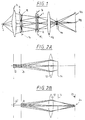
- FIG 1 is a schematic diagram of the beam path of a system with two faceted optical elements shown in refractive representation.
- the Light from the light source 1 is collected with the aid of a collector lens 3 and converted into a parallel or convergent bundle of light.
- the Raster elements of the first optical element 4 the following also are referred to as field honeycombs 5 and on a first honeycomb plate 7 are arranged, disassemble the tufts of light and produce at the location of the Raster elements 9 of the second optical element 8 with raster elements 9, which are arranged on a plate 10, secondary light sources 11.
- Die Raster elements 9 of the second optical element 8 are shown below also called pupil honeycomb.
- the field lens 12 forms the secondary Light sources in the exit pupil 24 'of the lighting system or the Entry pupil 100 of the following lens, not shown.
- the entrance pupil 100 of the objective coincides with the exit pupil 24 of the lens Lighting system together.
- Such an arrangement stands out through an intertwined beam path from the field and pupil levels of the light source 1 to the entrance pupil 100 of the objective.
- Kohler lighting is used as for example from Lexikon der Optik, Leipzig, 1990, p. 183.
- the field honeycomb 5 as well as the pupil honeycomb 9 are shown in the Embodiment designed collectively and have a prismatic Effect on. Both properties are shown separately in Figure 1.
- the lighting system according to FIG. 1 is then section by section considered. Since the interface is the light and aperture distribution in the The level of the honeycomb is independent of the consideration Source type and the collector mirror.
- FIGS. 2A and 2B for the central honeycomb pair 5, 9, the field and Drawn in pupil illustration.
- the pupil honeycomb 9 and Field lens 12 is the field honeycomb 5 on the reticle 14 or the image to be imaged Mask shown.
- the geometric expansion of the field honeycomb 5 determines the shape of the illuminated field in the reticle plane 14.
- the aspect ratio corresponds to Feldwaben 5 the ratio of arc length to ring width of required ring field in the object or reticle plane 14.
- the ring field is shaped by the field lens, as shown in FIGS. 5a-5b. Without As shown in FIG. 3, the field lens results in the reticle plane 14 Rectangular field.
- the image scale is approximated by the ratio of the Distances pupil honeycomb 9 - reticle plane 14 and field honeycomb 5 - pupil honeycomb Given 9.
- the optical effect of the honeycomb 5 is designed so that on Location of the pupil honeycomb 9 creates an image of the light source 1, which follows also be referred to as secondary light sources 11.
- the task of the field lens 12 is that secondary light sources 11 in the exit pupil 24 of the Lighting system 26, in the present case with the entrance pupil of the Lens coincides. Bring one into the beam path Field lens 12, so the field image is influenced in such a way that it the ring field is formed by controlling the distortion. The This does not change the imaging scale of the field honeycomb.
- FIG. 3 shows an embodiment of the invention in which the light source 1 a plasma light source is shown.
- the system is pure built reflective and shown without field mirror.
- the lighting system includes in the present embodiment as Light source is a pinch plasma source 1, as an EUV collector Collector mirror 3, which collects the light and into the field honeycomb plate 7 reflected, a pupil honeycomb plate 11 and a reticle in one Reticle level 14. The light turns to by reflection on the field honeycomb 5 the respective pupil honeycomb 9 of the pupil honeycomb plate 11 and thence to reticle level 14.
- the Exit pupil of the lighting system is not shown in Figure 3.
- the light source is used without Limitation to a highly directed light source.
- Such Light source is a synchrotron light source in the EUV area.
- the system has a dispersing element 33.
- the beam emanating from the light source is transmitted through the collector lens 3 directed to the first lens array 4 with raster elements.
- the Refractive embodiment shown includes the first lens array 4 with Raster elements a honeycomb plate 7, on which a variety of honeycombs 5 is arranged.
- the individual field honeycombs 5 have a prismatic one Effect on and thus form a variety of levels 35 secondary light sources 11.
- In the plane 35 is a second lens array 8 arranged with grid elements.
- This second lens array 8 also comprises a honeycomb panel 10.
- the arranged on the second honeycomb panel Raster elements are pupil honeycombs 9.
- the prismatic effect of the Raster elements 5 of the first lens array 4 is selected so that the secondary light sources 11, each with a specific pupil honeycomb 9 on the second lens array 8 coincides with raster elements.
- each field honeycomb 5 is a pupil honeycomb 9 of the assigned to the respective settings.
- a bundle of light, which by a Field honeycomb 5 and a certain pupil honeycomb 9 falls in the referred to the present application as a channel.
- the number of possible Channel N is 5 on the number of illuminated field honeycombs Field honeycomb plate 7 specified. Since in the illustrated embodiment in the pupil honeycomb plate 10 all adjustable illuminations in the Exit pupil 24 are held, the number of pupil honeycombs 9th on the pupil honeycomb plate 10 always larger than the number of channels. The Illumination of only certain pupil honeycombs 9 on the pupil honeycomb plate 10 leads to segmented or dividedled illumination in the Exit pupil 24.
- the light that passes through the selected pupil honeycomb 9 is with the help the field lens 12, which is close to the object or reticle plane 14 located.
- the images of the field honeycombs overlap in the reticle plane 14 5.
- the images 39 of the secondary light sources 11 fill the exit pupil 24 of the lighting system that doesn't work with the entrance pupil of the shown objective coincides, in a segmented manner.
- the segmentation of the images of the secondary light sources 39 in the Exit pupil 24 is a direct mirror image of the illuminated one Pupil honeycomb 9 in the plane 35 and thus the selection thereof the field combs 5.
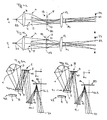
- FIGS. 5a and 5b show reflective versions of the invention shown. From the effect of the same components as in the in the Figures 4a to 4b shown refractive embodiment are with the same reference numbers. Instead of a lens array for the first and second optical elements 4.8 with raster elements, these are in reflective embodiment mirror with grid elements 5.9.
- the Raster elements or facets 5,9 are on honeycomb plates 7,10 under one certain tilt angle arranged. If you change the tilt angle of the individual field honeycomb 5 on the field honeycomb plate 7 and thus the prismatic effect of the field honeycomb 5, so the assignment of Field honeycomb 5 to the pupil honeycomb 9 on the pupil honeycomb plate and thus analogous to the refractive system shown in FIGS. 4a and 4b Illumination in the exit pupil 24 can be changed.
- the first mirror with grid elements shown as an example differently tilted field honeycombs 5 on the honeycomb plate 7 are 4.1 and 4.2.
- a change in the tilt angle of the field honeycombs could can be brought about by actuators directly on the honeycomb panel or by exchanging the mirror 4.1 for the mirror 4.2, which is characterized by the at different tilt angles on the field honeycomb plate of the mirror distinguish arranged field honeycombs.
- a field lens reflective system as a field imaging and field forming group a normal incidence field mirror 12.1 and a grazing incidence field mirror 12.2 used.
- the reticle is 50 inches on a reticle carrier arranged movable in the y direction.
- Figures 4a to 4b and 5a to 5b illustrate that by simple Exchange of the honeycomb panel 7 and selection of the illuminated Pupillary honeycomb 9 on the pupil honeycomb plate 10, the illumination in the Exit pupil 24 of the lighting system can be influenced.
- the field honeycombs can have 5 mirror elements be collecting effect.
- the collecting effect fully transferred to the collector mirror and the field honeycombs be designed as facets.
- the honeycombs of the honeycomb panels of different mirrors Raster elements have different prismatic effects, so how can shown in Figures 5a-5b, by exchanging a mirror with Raster elements against another mirror with raster elements different illuminations can be realized in the exit pupil 24.
- the prismatic effect of individual field honeycombs can be one Mirror by changing the tilt angle, for example with actuators respective field honeycomb on the field honeycomb plate of the mirror with Raster elements can be achieved.
- the pupil honeycombs To light rays in the field plane, which are with the reticle plane 14 coincides to overlap, the pupil honeycombs also have one prismatic effect on or with reflective systems Angle of inclination of the pupil honeycombs on the pupil honeycomb plate 11 set accordingly.
- the field honeycombs 5 can either have an isotropic optical effect and then have the same aspect ratio as that at the field level 14 field to be illuminated or they have an anisotropic effect. Then the aspect ratio of the field honeycomb is different from Aspect ratio of the field, usually the aspect ratio is the Field combs less than the aspect ratio of the field.
- FIG. 6a shows a top view of an example of a field honeycomb plate 7 a total of 72 grid elements in lines 60.1, 60.2 ... and each other are shifted.
- 6b.1 - 6b.3 show a plan view of a pupil honeycomb plate, where for each of the different illumination settings, namely circular setting, ring-shaped or annular setting and quadrupole setting the 72 channels of the honeycomb panel are available. For one Conventional lighting must be uniform across all 72 channels Field honeycombs are distributed. Ideally, the pupil honeycombs are all the same large or at least so large that they are each from an image of the secondary light sources are not fully illuminated.
- FIG. 9 shows a quadrupole setting with four ring circle segments as Illumination.
- the different settings of the lighting distribution in the Exit pupil according to the invention by exchanging the Field honeycomb panel or changing the angle of inclination of the individual Field honeycombs can be reached on the field honeycomb panel.
- FIG system A complete EUV lighting system is shown in FIG system according to the invention for adjusting the illumination in the Exit pupil 24 of the lighting system 26 that with the entrance pupil 100 of the lens 102 coincides, is shown.
- the system includes a light source 1, a collector mirror 3 for collecting the light of the Light source 1, a first optical element 4 with raster elements 5, a second optical element 8 with raster elements 9 and three field-shaping mirrors 12.1, 12.2, 12.3, the second optical Element 8 with grid elements 9 are subordinate and essentially serve to shape the field in the reticle plane 14.
- the reticle in the In the present case, reticle plane 14 is a reflection mask.
- the reticle is in the EUV system designed as a scanning system in the y direction traversable.
- the further carrier system 104 is a plane parallel to the reticle plane perpendicular to the y direction, that is movable in the x direction in the present example.
- This can different honeycomb panels are placed in the beam path and so different light channels between the first optical Element with raster elements and the second optical element with Raster elements and thus illuminations of the exit pupil of the Illumination system with the entrance pupil 100 of the following Objective 102 coincides, can be realized.
- the projection lens below is a 6 mirror projection lens, 106, such as shown in U.S. Patent Application 09 / 503,640, the full disclosure of which in the present application is recorded.
- the object 108 to be exposed is also located on a carrier system 110 that can be moved.
- the mirror 112.1, 112.2, 112.3, 112.4, 112.5, 112.6 of the projection lens centered on the common optical axis HA.
- the ring-shaped object field is arranged off-axis in the reticle plane 14.
- the light beam between Reticle and the first mirror of the projection lens is for optical Axis of the projection lens convergent.
- the main beam angles with Relative to the normal of the reticle are preferably between 5 ° and 7 °.
Landscapes
- Physics & Mathematics (AREA)
- General Physics & Mathematics (AREA)
- Engineering & Computer Science (AREA)
- General Engineering & Computer Science (AREA)
- High Energy & Nuclear Physics (AREA)
- Health & Medical Sciences (AREA)
- Chemical & Material Sciences (AREA)
- Epidemiology (AREA)
- Public Health (AREA)
- Nanotechnology (AREA)
- Environmental & Geological Engineering (AREA)
- Spectroscopy & Molecular Physics (AREA)
- Atmospheric Sciences (AREA)
- Mathematical Physics (AREA)
- Theoretical Computer Science (AREA)
- Toxicology (AREA)
- Crystallography & Structural Chemistry (AREA)
- Life Sciences & Earth Sciences (AREA)
- Exposure And Positioning Against Photoresist Photosensitive Materials (AREA)
- Exposure Of Semiconductors, Excluding Electron Or Ion Beam Exposure (AREA)
- Lenses (AREA)
- Microscoopes, Condenser (AREA)
- Non-Portable Lighting Devices Or Systems Thereof (AREA)
Abstract
Description


- Figur 1:
- Prinzipskizze des Strahlenganges eines Systems mit zwei optischen Elementen mit Rasterelementen
- Figuren 2a u. 2b:
- Feld- und Pupillenabbildung für das zentrale Wabenpaar
- Figur 3:
- Prinzipskizze des Strahlenganges eines Systems mit zwei Spiegeln mit Rasterelementen und Kollektoreinheit
- Figuren 4a - 4b:
- Strahlengang in einem refraktiven System mit zwei Linsen mit Rasterelementen mit einer ersten und einer zweiten Anordnung der Rasterelemente auf der ersten Linse, ergebend zwei unterschiedliche Ausleuchtungen
- Figuren 5a - 5b:
- Strahlengang in einem reflektiven System mit zwei Spiegeln mit Rasterelementen mit einer ersten und einer zweiten Anordnung der Rasterelemente auf dem ersten Spiegel
- Figur 6a:
- Draufsicht auf eine Feldwabenplatte mit 72 Feldwaben
- Figur 6b.1
- Draufsicht auf eine Pupillenwabenplatte gemäß der Erfindung mit 200 Pupillenwaben bei kreisförmiger Ausleuchtung
- Figur 6b.2
- Draufsicht auf eine Pupillenwabenplatte gemäß der Erfindung mit 200 Pupillenwaben bei ringförmiger Ausleuchtung
- Figur 6b.3
- Draufsicht auf eine Pupillenwabenplatte gemäß der Erfindung mit 200 Pupillenwaben bei quadropolarer Ausleuchtung
- Figur 7:
- kreisförmige Ausleuchtung der Austrittspupille eines erfindungsgemäßen Systems
- Figur 8:
- ringförmige Ausleuchtung der Austrittspupille eines erfindungsgemäßen Systems
- Figur 9:
- Quadrupol-Ausleuchtung des erfindungsgemäßen Systems
- Figur 10:
- Aufbau eines EUV-Projektionssystems mit einem erfindungsgemäßen Beleuchtungssystem
- 1:
- Lichtquelle
- 3:
- Kollektorlinse
- 4:
- erstes optisches Element
- 4.1.:
- erster Spiegel mit Rasterelementen in einer ersten Anordnung
- 4.2:
- erster Spiegel mit Rasterelementen in einer zweiten Anordnung
- 5:
- Feldwaben
- 7:
- erste Wabenplatte
- 8:
- zweites optisches Element
- 9:
- Pupillenwaben
- 10:
- zweite Wabenplatte
- 11:
- sekundäre Lichtquellen
- 12:
- Feldlinse
- 12.1:
- normal incidence Feldspiegel
- 12.2:
- grazing incidence Feldspiegel
- 12.3:
- normal incidence Feldspiegel
- 14:
- Retikelebene
- 24:
- Austrittspupille des Beleuchtungssystems
- 26:
- Beleuchtungssystem
- 33:
- Zerstreuelement
- 35:
- Ebene der sekundären Lichtquellen 11
- 39:
- Bilder der sekundären Lichtquellen
- 50:
- Retikelträger
- 60.1, 60.2..:
- Zeilen der Feldwabenplatte
- 100:
- Eintrittspupille des Objektives
- 102:
- Projektionsobjektiv
- 104:
- weiteres Trägersystem
- 106:
- 6-Spiegel Projektionsobjektiv
- 108:
- zu belichtendes Objekt
- 110:
- Trägersystem für das Objekt
- 112.1, 112.2, 112.3, 112.4, 112.5, 112.6:
- Spiegel des Projetionsobjektives
- HA:
- optische Achse des Projektionsobjektives
- x-Richtung:
- Verschieberichtung des Trägersystems der unterschiedlichen Feldwabenplatten
- y-Richtung:
- Scanrichtung des Retikels
Claims (26)
- Beleuchtungssystem für Wellenlängen ≤ 193 nm, insbesondere für die EUV-Lithographie, mit1.1 einer Lichtquelle (1)1.2 einer Objektebene (14)1.3 einer Austrittspupille (24)1.4 einem ersten optischen Element mit Rasterelementen (5), das durch die Lichtquelle (1) ausgeleuchtet wird und daß das von der Lichtquelle (1) her einfallende Lichtbündel in Lichtkanäle zerlegt1.5 einem zweiten optischen Element mit Rasterelementen (9), wobei jedem Lichtkanal, der von dem Rasterelement (5) des ersten optischen Elementes ausgebildet wird, ein Rasterelement (9) des zweiten optischen Elementes zugeordnet ist,
wobei1.6 die Rasterelemente (5, 9) des ersten optischen Elementes und des zweiten optischen Elementes jeweils Lichtkanälen zugeordnet sind, und die Rasterelemente (6, 9) derart ausgestaltet oder angeordnet werden, daß sich für jeden Lichtkanal ein durchgehender Strahlverlauf von der Lichtquelle (1) bis zur Objektebene (14) ergibt dadurch gekennzeichnet, daß1.7 die Zuordnung derart manipulierbar ist, daß durch die Zuordnung der Rasterelemente des ersten und des zweiten optischen Elementes eine vorgegebene Ausleuchtung in der Austrittspupille des Beleuchtungssystems eingestellt wird. - Beleuchtungssystem nach Anspruch 1, dadurch gekennzeichnet, daß das zweite optische Element eine derartige Anzahl an Rasterelementen umfaßt, daß mindestens zwei vorgegebene Ausleuchtungen durch Änderung der Zuordnung der Rasterelemente des ersten optischen Elementes zu den Rasterelementen des zweiten optischen Elementes eingestellt werden können, ohne daß das zweite optische Element getauscht werden muß.
- Beleuchtungsssystem nach Anspruch 2, dadurch gekennzeichnet, daß
das erste optische Element mit Rasterelementen austauschbar ist und durch Tausch des ersten optischen Elementes eine andere Zuordnung der Rasterelemente des ersten optischen Elementes zu den Rasterelementen des zweiten optischen Elementes und damit eine andere Ausleuchtung in der Austrittspupille realisiert wird. - Beleuchtungsssystem nach Anspruch 3, dadurch gekennzeichnet, daß
das Beleuchtungssystem eine Verschiebeeinrichtung mit einem Verschiebetisch umfaßt, auf dem eine Vielzahl von ersten optischen Elementen angeordnet ist, so daß durch Verschieben des Verschiebetisches die ersten optischen Elemente austauschbar sind. - Beleuchtungssystem nach einem der Ansprüche 1 bis 4, dadurch gekennzeichnet, daß
die Anzahl M der Rasterelemente (9) des zweiten optischen Elementes größer ist als die Anzahl N der Rasterelemente (5) des ersten optischen Elementes. - Beleuchtungssystem nach Anspruch 2, dadurch gekennzeichnet, daß
die Rasterelemente (5, 9) des ersten optischen Elementes Spiegel-Facetten sind, die auf einer Platte (7) angeordnet sind und der Lichtkanal zwischen den Rasterelementen des ersten und des zweiten optischen Elementes durch Verkippen der Spiegel-Facetten des ersten optischen Elementes in bezug auf die Plattenebene einstellbar ist, um so unterschiedliche Zuordnungen der Rasterelemente des ersten optischen Elementes zu den Rasterelementen des zweiten optischen Elementes und damit unterschiedliche Ausleuchtungen der Austrittspupille zu realisieren. - Beleuchtungssystem nach Anspruch 1, dadurch gekennzeichnet, daß
das zweite optische Element mit Rasterelementen austauschbar ist und mit jedem zweiten optischen Element mindestens eine bestimmte Ausleuchtung in der Austrittspupille realisiert wird, so daß durch Tausch des zweiten optischen Elementes eine andere Zuordnung der Rasterelemente eines ersten optischen Elementes zu den Rasterelementen des zweiten optischen Elementes realisiert wird. - Beleuchtungssystem nach Anspruch 7,
dadurch gekennzeichnet, daß
das erste optische Element mit Rasterelementen austauschbar ist. - Beleuchtungssystem nach Anspruch 7,
dadurch gekennzeichnet, daß die Rasterelemente des ersten optischen Elementes Spiegelfacetten sind und der Kipp der Spiegelfacetten des ersten optischen Elementes veränderbar ist. - Beleuchtungssystem nach Anspruch 1,
dadurch gekennzeichnet, daß
die Rasterelemente des zweiten optischen Elementes Spiegelfacetten sind und die Spiegelfacetten verschiebbar und kippbar sind, um durch Verschieben und Kippen der Spiegelfacetten eine andere Zuordnung der Rasterelemente eines ersten optischen Elementes zu den Rasterelementen des zweiten optischen Elementes realisiert wird. - Beleuchtungssystem nach Anspruch 10,
dadurch gekennzeichnet, daß
das erste optische Element mit Rasterelementen austauschbar ist. - Beleuchtungssystem nach Anspruch 10,
dadurch gekennzeichnet, daß die Rasterelemente des ersten optischen Elementes Spiegelfacetten sind und daß der Kipp der Spiegelfacetten des ersten optischen Elementes veränderbar ist. - Beleuchtungssystem nach einem der Ansprüche 1 bis 12,
dadurch gekennzeichnet, daß die Rasterelemente des ersten optischen Elementes in die Objektebene abgebildet werden und die Lichtkanäle sich in der Objektebene (14) überlagern. - Beleuchtungssystem nach einem der Ansprüche 1 bis 13, dadurch gekennzeichnet, daß
die Rasterelemente (5) des ersten optischen Elementes in oder in der Nähe der Rasterelemente des zweiten optischen Elementes sekundäre Lichtquellen erzeugen. - Beleuchtungssystem nach einem der Ansprüche 1 bis 14, dadurch gekennzeichnet, daß
das Beleuchtungssystem eine Kollektoreinheit vor dem ersten Spiegel mit Rasterelementen umfaßt. - Beleuchtungssystem nach einem der Ansprüch 1 bis 15,
dadurch gekennzeichnet, daß
das System wenigstens einen Spiegel oder eine Linse (12), der dem zweiten optischen Element mit Rasterelementen nachgeordnet ist, umfaßt, wobei der wenigstens eine Spiegel oder Linse eine Ebene, die in oder in der Nähe des zweiten optischen Elementes angeordnet ist, in die Austrittspupille abbildet. - Belechtungssystem nach einem der Ansprüche 1 bis 16
dadurch gekennzeichnet, daß
die Rasterelemente des zweiten optischen Elementes und wenigstens ein Spiegel oder eine Linse, der dem zweiten optischen Element mit Rasterelementen nachgeordnet ist, die ersten Rasterelemente in die Objektebene abbilden. - Beleuchtungssystem nach einem der Ansprüche 1 bis 17, dadurch gekennzeichnet, daß
die Lichtkanäle zwischen dem ersten optischen Element mit Rasterelementen und dem zweiten optischen Element mit Rasterelementen derart ausgebildet werden, daß die Ausleuchtung in der Austrittspupille kreisförmig ist. - Beleuchtungssystem nach einem der Ansprüche 1 bis 17, dadurch gekennzeichnet, daß
die Lichtkanäle zwischen dem ersten optischen Element mit Rasterelementen und dem zweiten optischen Element mit Rasterelementen derart ausgebildet werden, daß die Ausleuchtung in der Austrittspupille ringförmig ist. - Beleuchtungssystem nach einem der Ansprüche 1 bis 17, dadurch gekennzeichnet, daß
die Lichtkanäle zwischen dem ersten optischen Element mit Rasterelementen und dem zweiten optischen Element mit Rasterelementen derart ausgebildet werden, daß in der Austrittspupille eine Anzahl von Segmenten, die deutlich voneinander getrennt sind, ausgeleuchtet werden. - Beleuchtungssystem nach Anspruch 20,
dadurch gekennzeichnet, daß
die Anzahl der Segmente eine gerade Anzahl von Segmenten, insbesondere zwei oder vier Segmente ist. - Verfahren zur Einstellung einer Beleuchtungsverteilung in der Austrittspupille eines Beleuchtungssystems für Wellenlängen ≤ 193 nm, insbesondere für die EUV-Lithographie mit einem Beleuchtungssystem gemäß einem der Ansprüche 1 bis 21, dadurch gekennzeichnet, daß
eine vorgegebene Lichtverteilung in der Austrittspupille durch Tausch des ersten und/oder zweiten Elementes mit Rasterelementen und/oder durch Ändern der prismatischen Wirkung und der Anordnung der Rasterelemente des ersten und/oder zweiten optischen Elementes, insbesondere Verkippen und/oder Verschieben der Rasterelemente des ersten und/oder zweiten optischen Elementes eingestellt wird, wobei je nach der vorgegebenen Lichtverteilung in der Austrittspupille die Lichtkanäle zwischen den Rasterelementen des ersten und des zweiten optischen Elementes eingestellt werden. - EUV-Projektionsbelichtungsanlage für die Mikrolithographie miteiner Quelle zur Erzeugung von EUV-Strahlungeinem Beleuchtungssystem gemäß einem der Ansprüche 1 - 21 mit einer Austrittspupille, welches die von der Quelle erzeugte Strahlung teilweise sammelt und zur Beleuchtung eines Ringfeldes weiterleiteteiner strukturtragenden Maske auf einem Trägersystem, wobei diese Maske in der Ebene des Ringfeldes liegteiner Projektionseinrichtung, insbesondere einem Projektionsobjektiv mit einer Eintrittspupille, die mit der Austrittspupille des Beleuchtungssystems zusammenfällt, wobei dieses Projektionsobjektiv den beleuchteten Teil der strukturtragenden Maske in ein Bildfeld abbildetein lichtsensitives Substrat auf einem Trägersystem, wobei dieses lichtsensitive Substrat in der Ebene des Bildfeldes der Projektionseinrichtung liegt.
- EUV-Projektionsbelichtungsanlage gemäß Anspruch 23, dadurch gekennzeichnet, daß
die Projektionsbelichtungsanlage ein Scanning-System ist, wobei das Trägersystem für die strukturtragende Maske in der Ringfeldebene in einer ersten Richtung verfahrbar ist. - EUV-Projektionsbelichtungsanlage gemäß Anspruch 24, dadurch gekennzeichnet, daß
die Projektionsbelichtungsanlage ein oder mehrere weitere Trägersysteme zur Aufnahme von mehreren ersten und/oder zweiten optischen Elementen umfaßt, die in einer zweiten Richtung verfahrbar sind und daß die erste Richtung senkrecht auf der zweiten Richtung steht. - Verfahren zur Herstellung von mikroelektronischen Bauelementen, insbesondere Halbleiterchips mit einer EUV-Projektionsbelichtungsanlage gemäß einem der Ansprüche 24 bis 25.
Applications Claiming Priority (2)
| Application Number | Priority Date | Filing Date | Title |
|---|---|---|---|
| DE10053587A DE10053587A1 (de) | 2000-10-27 | 2000-10-27 | Beleuchtungssystem mit variabler Einstellung der Ausleuchtung |
| DE10053587 | 2000-10-27 |
Publications (2)
| Publication Number | Publication Date |
|---|---|
| EP1202101A2 true EP1202101A2 (de) | 2002-05-02 |
| EP1202101A3 EP1202101A3 (de) | 2004-02-25 |
Family
ID=7661440
Family Applications (1)
| Application Number | Title | Priority Date | Filing Date |
|---|---|---|---|
| EP01123629A Withdrawn EP1202101A3 (de) | 2000-10-27 | 2001-10-02 | Beleuchtungssystem mit variabler Einstellung der Ausleuchtung |
Country Status (5)
| Country | Link |
|---|---|
| US (3) | US6658084B2 (de) |
| EP (1) | EP1202101A3 (de) |
| JP (1) | JP4077619B2 (de) |
| KR (1) | KR100842426B1 (de) |
| DE (2) | DE10053587A1 (de) |
Cited By (15)
| Publication number | Priority date | Publication date | Assignee | Title |
|---|---|---|---|---|
| EP1280008A3 (de) * | 2001-07-27 | 2004-05-26 | Canon Kabushiki Kaisha | Belichtungssystem, Projektionsbelichtungsapparat und Verfahren zur Herstellung eines Artikels |
| US6771352B2 (en) | 2002-03-18 | 2004-08-03 | Asml Netherlands B.V. | Lithographic apparatus and device manufacturing method |
| EP1349009A3 (de) * | 2002-03-18 | 2004-12-22 | ASML Netherlands B.V. | Lithographischer Apparat und Verfahren zur Herstellung eines Artikels |
| JP2007500432A (ja) * | 2003-07-30 | 2007-01-11 | カール・ツァイス・エスエムティー・アーゲー | マイクロリソグラフィの照明システム |
| US7170587B2 (en) | 2002-03-18 | 2007-01-30 | Asml Netherlands B.V. | Lithographic apparatus and device manufacturing method |
| US7405871B2 (en) | 2005-02-08 | 2008-07-29 | Intel Corporation | Efficient EUV collector designs |
| US7417708B2 (en) | 2002-10-25 | 2008-08-26 | Nikon Corporation | Extreme ultraviolet exposure apparatus and vacuum chamber |
| DE102007025846A1 (de) | 2007-06-01 | 2008-12-11 | Carl Zeiss Smt Ag | Beleuchtungssystem mit wenigstens einem akustooptischen Spiegel |
| WO2008145364A3 (de) * | 2007-05-31 | 2009-01-29 | Zeiss Carl Smt Ag | Verfahren zur herstellung eines optischen elementes mit hilfe von abformung, optisches element hergestellt nach diesem verfahren, kollektor und beleuchtungssystem |
| DE102008054429A1 (de) | 2008-01-11 | 2009-07-16 | Carl Zeiss Smt Ag | Schwingungsentkoppelte Lagerung eines Bauteils in einer Vakuumkammer |
| WO2010099807A1 (de) * | 2009-03-06 | 2010-09-10 | Carl Zeiss Smt Ag | Beleuchtungsoptik sowie optische systeme für die mikrolithographie |
| DE102010062720A1 (de) | 2010-12-09 | 2012-06-14 | Carl Zeiss Smt Gmbh | EUV-Lithographiesystem |
| DE102011088152A1 (de) | 2011-12-09 | 2013-06-13 | Carl Zeiss Smt Gmbh | EUV-Lithographiesystem |
| DE102012218221A1 (de) | 2012-10-05 | 2014-04-10 | Carl Zeiss Smt Gmbh | Monitorsystem zum Bestimmen von Orientierungen von Spiegelelementen und EUV-Lithographiesystem |
| US9304408B2 (en) | 2008-03-20 | 2016-04-05 | Carl Zeiss Smt Gmbh | Projection objective for microlithography |
Families Citing this family (139)
| Publication number | Priority date | Publication date | Assignee | Title |
|---|---|---|---|---|
| US6859328B2 (en) * | 1998-05-05 | 2005-02-22 | Carl Zeiss Semiconductor | Illumination system particularly for microlithography |
| US7441017B2 (en) * | 2001-06-29 | 2008-10-21 | Thomas Lee Watson | System and method for router virtual networking |
| US7333178B2 (en) * | 2002-03-18 | 2008-02-19 | Asml Netherlands B.V. | Lithographic apparatus and device manufacturing method |
| DE10220324A1 (de) * | 2002-04-29 | 2003-11-13 | Zeiss Carl Smt Ag | Projektionsverfahren mit Pupillenfilterung und Projektionsobjektiv hierfür |
| DE10219514A1 (de) * | 2002-04-30 | 2003-11-13 | Zeiss Carl Smt Ag | Beleuchtungssystem, insbesondere für die EUV-Lithographie |
| DE10305573B3 (de) * | 2002-10-11 | 2004-07-01 | Aixuv Gmbh | Vorrichtung und Verfahren zur Testbestrahlung von mit photoempfindlichen Lacken beschichteten Objekten |
| US7378666B2 (en) | 2002-10-11 | 2008-05-27 | Qimonda Ag | Irradiation device for testing objects coated with light-sensitive paint |
| DE10317667A1 (de) * | 2003-04-17 | 2004-11-18 | Carl Zeiss Smt Ag | Optisches Element für ein Beleuchtungssystem |
| US7714983B2 (en) * | 2003-09-12 | 2010-05-11 | Carl Zeiss Smt Ag | Illumination system for a microlithography projection exposure installation |
| WO2005078522A2 (en) * | 2004-02-17 | 2005-08-25 | Carl Zeiss Smt Ag | Illumination system for a microlithographic projection exposure apparatus |
| JP4551666B2 (ja) * | 2004-02-19 | 2010-09-29 | キヤノン株式会社 | 照明装置及び露光装置 |
| US7283209B2 (en) * | 2004-07-09 | 2007-10-16 | Carl Zeiss Smt Ag | Illumination system for microlithography |
| US7511798B2 (en) * | 2004-07-30 | 2009-03-31 | Asml Holding N.V. | Off-axis catadioptric projection optical system for lithography |
| US8134687B2 (en) * | 2004-08-23 | 2012-03-13 | Carl Zeiss Smt Gmbh | Illumination system of a microlithographic exposure apparatus |
| US7136214B2 (en) * | 2004-11-12 | 2006-11-14 | Asml Holding N.V. | Active faceted mirror system for lithography |
| DE102005042005A1 (de) | 2004-12-23 | 2006-07-06 | Carl Zeiss Smt Ag | Hochaperturiges Objektiv mit obskurierter Pupille |
| JP2006253487A (ja) * | 2005-03-11 | 2006-09-21 | Nikon Corp | 照明装置、投影露光方法、投影露光装置、及びマイクロデバイスの製造方法 |
| JP2008544531A (ja) * | 2005-06-21 | 2008-12-04 | カール ツァイス エスエムテー アーゲー | 瞳ファセットミラー上に減衰素子を備えた二重ファセット照明光学系 |
| EP1938150B1 (de) * | 2005-10-18 | 2011-03-23 | Carl Zeiss SMT GmbH | Kollektor für beleuchtungssysteme mit einer wellenlänge </= 193 nm |
| JP2007150295A (ja) | 2005-11-10 | 2007-06-14 | Carl Zeiss Smt Ag | ラスタ要素を有する光学装置、及びこの光学装置を有する照射システム |
| JP5068271B2 (ja) * | 2006-02-17 | 2012-11-07 | カール・ツァイス・エスエムティー・ゲーエムベーハー | マイクロリソグラフィ照明システム、及びこの種の照明システムを含む投影露光装置 |
| DE102006017336B4 (de) * | 2006-04-11 | 2011-07-28 | Carl Zeiss SMT GmbH, 73447 | Beleuchtungssystem mit Zoomobjektiv |
| DE102006031654A1 (de) * | 2006-04-24 | 2007-10-25 | Carl Zeiss Smt Ag | Facettenspiegel mit einer Vielzahl von Spiegelsegmenten |
| DE102006020734A1 (de) * | 2006-05-04 | 2007-11-15 | Carl Zeiss Smt Ag | Beleuchtungssystem für die EUV-Lithographie sowie erstes und zweites optisches Element zum Einsatz in einem derartigen Beleuchtungssystem |
| WO2007138805A1 (ja) * | 2006-05-25 | 2007-12-06 | Nikon Corporation | 照明光学装置、露光装置、およびデバイス製造方法 |
| DE102006036064A1 (de) * | 2006-08-02 | 2008-02-07 | Carl Zeiss Smt Ag | Beleuchtungssystem für eine Projektionsbelichtungsanlage mit Wellenlängen ≦ 193 nm |
| DE102006039760A1 (de) * | 2006-08-24 | 2008-03-13 | Carl Zeiss Smt Ag | Beleuchtungssystem mit einem Detektor zur Aufnahme einer Lichtintensität |
| DE102006056035A1 (de) * | 2006-11-28 | 2008-05-29 | Carl Zeiss Smt Ag | Beleuchtungsoptik für die EUV-Projektions-Mikrolithographie, Beleuchtungssystem mit einer derartigen Beleuchtungsoptik, Projektionsbelichtungsanlage mit einem derartigen Beleuchtungssystem, Verfahren zur Herstellung eines mikrostrukturierten Bauteils sowie durch das Verfahren hergestelltes mikrostrukturiertes Bauteil |
| DE102006059024A1 (de) * | 2006-12-14 | 2008-06-19 | Carl Zeiss Smt Ag | Projektionsbelichtungsanlage für die Mikrolithographie, Beleuchtungsoptik für eine derartige Projektionsbelichtungsanlage, Verfahren zum Betrieb einer derartigen Projektionsbelichtungsanlage, Verfahren zur Herstellung eines mikrostrukturierten Bauteils sowie durch das Verfahren hergestelltes mikrostrukturiertes Bauteil |
| US7990520B2 (en) | 2006-12-18 | 2011-08-02 | Carl Zeiss Smt Gmbh | Microlithography illumination systems, components and methods |
| DE102007023411A1 (de) * | 2006-12-28 | 2008-07-03 | Carl Zeiss Smt Ag | Optisches Element, Beleuchtungsoptik für die Mikrolithographie mit mindestens einem derartigen optischen Element sowie Beleuchtungssystem mit einer derartigen Beleuchtungsoptik |
| US20080259298A1 (en) * | 2007-04-19 | 2008-10-23 | Asml Netherlands B.V. | Lithographic apparatus and device manufacturing method |
| US20080257883A1 (en) | 2007-04-19 | 2008-10-23 | Inbev S.A. | Integrally blow-moulded bag-in-container having an inner layer and the outer layer made of the same material and preform for making it |
| US9475611B2 (en) | 2007-04-19 | 2016-10-25 | Anheuser-Busch Inbev S.A. | Integrally blow-moulded bag-in-container having interface vents opening to the atmosphere at location adjacent to bag's mouth, preform for making it; and processes for producing the preform and bag-in-container |
| US20150266620A1 (en) | 2007-04-19 | 2015-09-24 | Anheuser-Busch Inbev S.A. | Integrally blow-moulded bag-in-container having a bag anchoring point; process for production thereof; and tool thereof |
| US20080259304A1 (en) * | 2007-04-20 | 2008-10-23 | Asml Netherlands B.V. | Lithographic apparatus and method |
| CN101669071B (zh) * | 2007-04-25 | 2012-03-21 | 卡尔蔡司Smt有限责任公司 | 微光刻曝光装置中照明掩模的照明系统 |
| US20080278698A1 (en) * | 2007-05-08 | 2008-11-13 | Asml Netherlands B.V. | Lithographic apparatus and method |
| US8237913B2 (en) * | 2007-05-08 | 2012-08-07 | Asml Netherlands B.V. | Lithographic apparatus and method |
| JP5077724B2 (ja) * | 2007-06-07 | 2012-11-21 | カール・ツァイス・エスエムティー・ゲーエムベーハー | マイクロリソグラフィツール用の反射照明システム |
| US20090040493A1 (en) * | 2007-08-09 | 2009-02-12 | Hideki Komatsuda | Illumination optical system, illumination optical apparatus, exposure apparatus, and device manufacturing method |
| DE102008041593A1 (de) | 2007-10-09 | 2009-04-16 | Carl Zeiss Smt Ag | Beleuchtungsoptik für die Mikrolithographie |
| DE102008013229B4 (de) | 2007-12-11 | 2015-04-09 | Carl Zeiss Smt Gmbh | Beleuchtungsoptik für die Mikrolithographie |
| DE102009000099A1 (de) | 2009-01-09 | 2010-07-22 | Carl Zeiss Smt Ag | Mikrospiegelarray mit Doppelbiegebalken Anordnung und elektronischer Aktorik |
| DE102008009600A1 (de) * | 2008-02-15 | 2009-08-20 | Carl Zeiss Smt Ag | Facettenspiegel zum Einsatz in einer Projektionsbelichtungsanlage für die Mikro-Lithographie |
| KR101591610B1 (ko) * | 2008-02-15 | 2016-02-03 | 칼 짜이스 에스엠티 게엠베하 | 마이크로리소그래피용 투영 노광 장치에 사용하기 위한 패싯 미러 |
| JP5074226B2 (ja) * | 2008-02-16 | 2012-11-14 | エスアイアイ・ナノテクノロジー株式会社 | 荷電粒子ビーム装置 |
| DE102008000788A1 (de) | 2008-03-20 | 2009-09-24 | Carl Zeiss Smt Ag | Beleuchtungssystem für eine Mikrolithographie-Projektionsbelichtungsanlage |
| DE102008000967B4 (de) | 2008-04-03 | 2015-04-09 | Carl Zeiss Smt Gmbh | Projektionsbelichtungsanlage für die EUV-Mikrolithographie |
| NL1036771A1 (nl) * | 2008-04-22 | 2009-10-26 | Asml Netherlands Bv | Illumination System and Lithographic Method. |
| DE102008001511A1 (de) | 2008-04-30 | 2009-11-05 | Carl Zeiss Smt Ag | Beleuchtungsoptik für die EUV-Mikrolithografie sowie Beleuchtungssystem und Projektionsbelichtungsanlage mit einer derartigen Beleuchtungsoptik |
| DE102008002749A1 (de) | 2008-06-27 | 2009-12-31 | Carl Zeiss Smt Ag | Beleuchtungsoptik für die Mikrolithografie |
| EP2146248B1 (de) | 2008-07-16 | 2012-08-29 | Carl Zeiss SMT GmbH | Beleuchtungssystem eines mikrolithografischen Projektionsbelichtungsgerätes |
| DE102008042462B4 (de) | 2008-09-30 | 2010-11-04 | Carl Zeiss Smt Ag | Beleuchtungssystem für die EUV-Mikrolithographie |
| KR101769157B1 (ko) | 2008-10-20 | 2017-08-17 | 칼 짜이스 에스엠테 게엠베하 | 방사선 빔 안내를 위한 광학 모듈 |
| DE102009034502A1 (de) | 2009-07-24 | 2011-01-27 | Carl Zeiss Smt Ag | Optische Baugruppe zur Führung eines EUV-Strahlungsbündels |
| DE102009009568A1 (de) | 2008-10-20 | 2010-04-29 | Carl Zeiss Smt Ag | Optische Baugruppe zur Führung eines EUV-Strahlungsbündels |
| NL2004831A (en) * | 2009-06-17 | 2010-12-20 | Asml Netherlands Bv | Lithographic apparatus and method. |
| DE102009030501A1 (de) | 2009-06-24 | 2011-01-05 | Carl Zeiss Smt Ag | Abbildende Optik zur Abbildung eines Objektfeldes in ein Bildfeld sowie Beleuchtungsoptik zur Ausleuchtung eines Objektfeldes |
| NL2004527A (en) | 2009-08-25 | 2011-02-28 | Asml Netherlands Bv | Optical apparatus, and method of orienting a reflective element. |
| JP2011077142A (ja) * | 2009-09-29 | 2011-04-14 | Nikon Corp | 照明光学装置、露光装置及びデバイス製造方法 |
| DE102009045135A1 (de) * | 2009-09-30 | 2011-03-31 | Carl Zeiss Smt Gmbh | Beleuchtungsoptik für die Mikrolithographie |
| DE102009045491A1 (de) | 2009-10-08 | 2010-11-25 | Carl Zeiss Smt Ag | Beleuchtungsoptik |
| DE102009045694B4 (de) * | 2009-10-14 | 2012-03-29 | Carl Zeiss Smt Gmbh | Beleuchtungsoptik für die Mikrolithographie sowie Beleuchtungssystem und Projektionsbelichtungsanlage mit einer derartigen Beleuchtungsoptik |
| DE202009015830U1 (de) | 2009-11-20 | 2010-03-11 | Noell Mobile Systems Gmbh | Modulares verfahrbares Meßportal |
| DE102009054540B4 (de) | 2009-12-11 | 2011-11-10 | Carl Zeiss Smt Gmbh | Beleuchtungsoptik für die EUV-Mikrolithographie |
| DE102009054888A1 (de) | 2009-12-17 | 2011-06-22 | Carl Zeiss SMT GmbH, 73447 | Optisches Element mit einer Mehrzahl von refletiven Facettenelementen |
| NL2005771A (en) | 2009-12-29 | 2011-06-30 | Asml Netherlands Bv | Illumination system, lithographic apparatus and illumination method. |
| DE102011004615A1 (de) * | 2010-03-17 | 2011-09-22 | Carl Zeiss Smt Gmbh | Beleuchtungsoptik für die Projektionslithografie |
| DE102010029765A1 (de) | 2010-06-08 | 2011-12-08 | Carl Zeiss Smt Gmbh | Beleuchtungsoptik für die EUV-Projektionslithografie |
| DE102010040108A1 (de) | 2010-09-01 | 2012-03-01 | Carl Zeiss Smt Gmbh | Obskurationsblende |
| DE102010040811A1 (de) * | 2010-09-15 | 2012-03-15 | Carl Zeiss Smt Gmbh | Abbildende Optik |
| DE102010041746A1 (de) | 2010-09-30 | 2012-04-05 | Carl Zeiss Smt Gmbh | Projektionsbelichtungsanlage der EUV-Mikrolithographie und Verfahren zur mikrolithographischen Belichtung |
| JP5644416B2 (ja) * | 2010-11-24 | 2014-12-24 | 株式会社ニコン | 光学ユニット、光学系、露光装置、及びデバイスの製造方法 |
| JP6016169B2 (ja) * | 2011-01-29 | 2016-10-26 | カール・ツァイス・エスエムティー・ゲーエムベーハー | マイクロリソグラフィ投影露光装置の照明系 |
| NL2008009A (en) * | 2011-02-02 | 2012-08-06 | Asml Netherlands Bv | Illumination system, lithographic apparatus and method. |
| DE102011005881A1 (de) * | 2011-03-22 | 2012-05-03 | Carl Zeiss Smt Gmbh | Verfahren zur Einstellung eines Beleuchtungssystems einer Projektionsbelichtungsanlage für die Projektionslithographie |
| DE102011076145B4 (de) | 2011-05-19 | 2013-04-11 | Carl Zeiss Smt Gmbh | Verfahren zum Zuordnen einer Pupillenfacette eines Pupillenfacettenspiegels einer Beleuchtungsoptik einer Projektionsbelichtungsanlage zu einer Feldfacette eines Feldfacettenspiegels der Beleuchtungsoptik |
| DE102011076460A1 (de) * | 2011-05-25 | 2012-11-29 | Carl Zeiss Smt Gmbh | Beleuchtungsoptik |
| DE102011076658A1 (de) | 2011-05-30 | 2012-05-10 | Carl Zeiss Smt Gmbh | Beleuchtungsoptik für die EUV-Projektionslithographie |
| US8823921B2 (en) * | 2011-08-19 | 2014-09-02 | Ultratech, Inc. | Programmable illuminator for a photolithography system |
| DE102011086328A1 (de) | 2011-11-15 | 2013-05-16 | Carl Zeiss Smt Gmbh | Spiegel zum Einsatz zur Führung von Beleuchtungs- und Abbildungslicht in der EUV-Projektionslithografie |
| DE102012201235B4 (de) | 2012-01-30 | 2013-08-29 | Carl Zeiss Smt Gmbh | Verfahren zum Einstellen einer Beleuchtungsgeometrie für eine Be-leuchtungsoptik für die EUV-Projektionslithographie |
| DE102012204142A1 (de) | 2012-03-16 | 2013-03-21 | Carl Zeiss Smt Gmbh | Kollektor |
| DE102012204273B4 (de) | 2012-03-19 | 2015-08-13 | Carl Zeiss Smt Gmbh | Beleuchtungsoptik für die EUV-Projektionslithografie |
| DE102012206609B4 (de) | 2012-04-23 | 2023-08-10 | Carl Zeiss Smt Gmbh | Strahlführungsoptik für ein Vielstrahlsystem sowie Verfahren |
| DE102012206612A1 (de) | 2012-04-23 | 2013-10-24 | Carl Zeiss Smt Gmbh | Optisches Bauelement zur Führung eines Strahlungsbündels |
| DE102012207866A1 (de) | 2012-05-11 | 2013-11-14 | Carl Zeiss Smt Gmbh | Baugruppe für eine Projektionsbelichtungsanlage für die EUV-Projektionslithografie |
| DE102012208064A1 (de) | 2012-05-15 | 2013-11-21 | Carl Zeiss Smt Gmbh | Beleuchtungsoptik für die EUV-Projektionslithographie |
| DE102012208514A1 (de) | 2012-05-22 | 2013-11-28 | Carl Zeiss Smt Gmbh | Justagevorrichtung sowie Masken-Inspektionsvorrichtung mit einer derartigen Justagevorrichtung |
| DE102012210073A1 (de) | 2012-06-15 | 2013-04-25 | Carl Zeiss Smt Gmbh | Beleuchtungsoptik für die EUV- Projektionslithographie |
| DE102012210174A1 (de) | 2012-06-18 | 2013-06-06 | Carl Zeiss Smt Gmbh | Optisches Bauelement |
| DE102012212453A1 (de) | 2012-07-17 | 2014-01-23 | Carl Zeiss Smt Gmbh | Beleuchtungsoptik |
| DE102012212664A1 (de) | 2012-07-19 | 2014-01-23 | Carl Zeiss Smt Gmbh | Verfahren zum Einstellen eines Beleuchtungssettings |
| DE102012213368A1 (de) * | 2012-07-30 | 2013-12-05 | Carl Zeiss Smt Gmbh | Beleuchtungsoptik für die EUV-Projektionslithographie |
| DE102012218105A1 (de) | 2012-10-04 | 2013-08-14 | Carl Zeiss Smt Gmbh | Vorrichtung zur Einkopplung von Beleuchtungsstrahlung in eine Beleuchtungsoptik |
| DE102012218074A1 (de) | 2012-10-04 | 2013-08-14 | Carl Zeiss Smt Gmbh | Blenden-Vorrichtung |
| DE102012220597A1 (de) | 2012-11-13 | 2014-05-28 | Carl Zeiss Smt Gmbh | Beleuchtungsoptik für die EUV-Projektionslithographie |
| DE102012220596A1 (de) | 2012-11-13 | 2014-05-15 | Carl Zeiss Smt Gmbh | Verfahren zum Zuordnen einer Pupillenfacette eines Pupillenfacettenspiegels einer Beleuchtungsoptik einer Projektionsbelichtungsanlage zu einer Feldfacette eines Feldfacettenspiegels der Beleuchtungsoptik |
| CN103092000A (zh) * | 2012-11-14 | 2013-05-08 | 北京理工大学 | 极紫外光刻复眼匀光离轴照明系统及实现离轴照明的方法 |
| DE102013203364A1 (de) | 2013-02-28 | 2014-09-11 | Carl Zeiss Smt Gmbh | Reflektierende Beschichtung mit optimierter Dicke |
| DE102013211268B4 (de) | 2013-06-17 | 2014-11-20 | Carl Zeiss Smt Gmbh | Beleuchtunsoptik für die lithografische Projektionsbelichtung |
| DE102013212363A1 (de) | 2013-06-27 | 2014-07-31 | Carl Zeiss Smt Gmbh | Facettenspiegel, insbesondere für die EUV-Projektionslithografie |
| DE102013218131A1 (de) * | 2013-09-11 | 2015-03-12 | Carl Zeiss Smt Gmbh | Beleuchtungsoptik sowie Beleuchtungssystem für die EUV-Projektionslithographie |
| DE102013218749A1 (de) | 2013-09-18 | 2015-03-19 | Carl Zeiss Smt Gmbh | Beleuchtungssystem sowie Beleuchtungsoptik für die EUV-Projektionslithografie |
| DE102013223808A1 (de) | 2013-11-21 | 2014-12-11 | Carl Zeiss Smt Gmbh | Optische Spiegeleinrichtung zur Reflexion eines Bündels von EUV-Licht |
| DE102013223935A1 (de) | 2013-11-22 | 2015-05-28 | Carl Zeiss Smt Gmbh | Beleuchtungssystem für die EUV-Belichtungslithographie |
| DE102014219649A1 (de) | 2013-11-22 | 2015-05-28 | Carl Zeiss Smt Gmbh | Anordnung einer Energiesensor-Einrichtung |
| CN103713389B (zh) * | 2013-12-11 | 2016-06-29 | 大族激光科技产业集团股份有限公司 | 激光器及其光斑调节组件 |
| DE102014222952A1 (de) | 2014-01-09 | 2015-07-23 | Carl Zeiss Smt Gmbh | Verfahren zum Herstellen eines Verbundstruktur, Verbundstruktur, insbesondere Facettenspiegel, und optische Anordnung damit |
| JP5854295B2 (ja) * | 2014-04-11 | 2016-02-09 | カール・ツァイス・エスエムティー・ゲーエムベーハー | マイクロリソグラフィ用の照明光学系及び光学系 |
| DE102014216801A1 (de) | 2014-08-25 | 2016-02-25 | Carl Zeiss Smt Gmbh | Facettenspiegel für eine Beleuchtungsoptik für die Projektionslithographie |
| DE102014217608A1 (de) | 2014-09-03 | 2014-11-20 | Carl Zeiss Smt Gmbh | Verfahren zum Zuordnen einer zweiten Facette eines im Strahlengang zweiten facettierten Elements einer Beleuchtungsoptik |
| DE102014223326B4 (de) | 2014-11-14 | 2018-08-16 | Carl Zeiss Smt Gmbh | Verfahren zur Vorhersage mindestens eines Beleuchtungsparameters zur Bewertung eines Beleuchtungssettings und Verfahren zur Optimierung eines Beleuchtungssettings |
| DE102014226917A1 (de) | 2014-12-23 | 2015-12-17 | Carl Zeiss Smt Gmbh | Beleuchtungssystem für die EUV-Projektionslithographie |
| DE102015200531A1 (de) | 2015-01-15 | 2016-02-18 | Carl Zeiss Smt Gmbh | Optisches Modul |
| KR102605161B1 (ko) | 2015-02-11 | 2023-11-23 | 칼 짜이스 에스엠티 게엠베하 | Euv 투영 리소그라피를 위한 조명 광학기기 |
| DE102015202411A1 (de) | 2015-02-11 | 2016-08-11 | Carl Zeiss Smt Gmbh | Beleuchtungsoptik für die EUV-Projektionslithografie |
| DE102015208571A1 (de) | 2015-05-08 | 2016-11-10 | Carl Zeiss Smt Gmbh | Beleuchtungsoptik für die EUV-Projektionslithografie |
| DE102016202736A1 (de) | 2015-04-17 | 2016-05-25 | Carl Zeiss Smt Gmbh | Beleuchtungsoptik für eine Projektionsbelichtungsanlage |
| DE102015208514A1 (de) | 2015-05-07 | 2016-11-10 | Carl Zeiss Smt Gmbh | Facettenspiegel für die EUV-Projektionslithografie sowie Beleuchtungsoptik mit einem derartigen Facettenspiegel |
| DE102015209175A1 (de) | 2015-05-20 | 2016-11-24 | Carl Zeiss Smt Gmbh | Pupillenfacettenspiegel |
| DE102016203990A1 (de) * | 2016-03-10 | 2017-09-14 | Carl Zeiss Smt Gmbh | Verfahren zum Herstellen eines Beleuchtungssystems für eine EUV-Projektionsbelichtungsanlage, Beleuchtungssystem und Messverfahren |
| DE102016214785A1 (de) | 2016-08-09 | 2018-02-15 | Carl Zeiss Smt Gmbh | Optisches Modul mit einer Antikollisionseinrichtung für Modulkomponenten |
| DE102016217479A1 (de) | 2016-09-14 | 2017-09-14 | Carl Zeiss Smt Gmbh | Optisches modul mit verkippbaren optischen flächen |
| DE102017200663A1 (de) | 2017-01-17 | 2017-03-02 | Carl Zeiss Smt Gmbh | Verfahren zur Zuordnung von Ausgangs-Kippwinkeln von kippbaren Feldfacetten eines Feldfacettenspiegels für eine Projektionsbelich-tungsanlage für die Projektionslithografie |
| DE102017202930A1 (de) | 2017-02-23 | 2017-04-13 | Carl Zeiss Smt Gmbh | Verfahren zur Regelung einer Beleuchtungsdosis einer Beleuchtung eines Objekt-feldes einer Projektionsbelichtungsanlage sowie Projektionsbelichtungsanlage zur Durchführung des Verfahrens |
| DE102017205548A1 (de) | 2017-03-31 | 2018-10-04 | Carl Zeiss Smt Gmbh | Optische Baugruppe zum Führen eines Ausgabestrahls eines Freie-Elektronen-Lasers |
| DE102017217251A1 (de) | 2017-09-27 | 2019-03-28 | Carl Zeiss Smt Gmbh | Verfahren und Anordnung zur Analyse der Wellenfrontwirkung eines optischen Systems |
| DE102018201457A1 (de) | 2018-01-31 | 2019-08-01 | Carl Zeiss Smt Gmbh | Beleuchtungsoptik für die Projektionslithographie |
| DE102018207410A1 (de) | 2018-05-14 | 2019-05-23 | Carl Zeiss Smt Gmbh | Facettenspiegel für eine Beleuchtungsoptik für die Projektionslithographie |
| DE102018215505A1 (de) | 2018-09-12 | 2018-10-31 | Carl Zeiss Smt Gmbh | Projektionsoptik für eine Projektionsbelichtungsanlage |
| DE102018220625A1 (de) | 2018-11-29 | 2020-06-04 | Carl Zeiss Smt Gmbh | Optisches Beleuchtungssystem für Projektionslithographie |
| DE102018221128A1 (de) | 2018-12-06 | 2020-06-10 | Carl Zeiss Smt Gmbh | Verfahren zum Tauschen eines Spiegels in einer Projektionsbelichtungsanlage sowie Lagedaten-Messeinrichtung zum Durchführen des Verfahrens |
| DE102019217507A1 (de) | 2019-02-04 | 2020-08-06 | Carl Zeiss Smt Gmbh | Facettenspiegel und Verfahren zu dessen Herstellung |
| DE102021201690A1 (de) | 2021-02-23 | 2022-08-25 | Carl Zeiss Smt Gmbh | Optisches System, insbesondere für die EUV-Lithographie |
| DE102022209214A1 (de) | 2022-09-05 | 2024-03-07 | Carl Zeiss Smt Gmbh | Einzelspiegel eines Pupillenfacettenspiegels und Pupillenfacettenspiegel für eine Beleuchtungsoptik einer Projektionsbelichtungsanlage |
| DE102023203095A1 (de) | 2023-04-04 | 2023-05-25 | Carl Zeiss Smt Gmbh | Verfahren zum Vorgeben einer Soll-Verteilung einer Beleuchtungs-Intensität über eine Feldhöhe eines Feldes einer Projektionsbelichtungsanlage |
| DE102024211125A1 (de) | 2024-11-20 | 2026-05-21 | Carl Zeiss Smt Gmbh | Feldfacettenspiegel für eine Beleuchtungsoptik für die EUV-Projektionslithographie |
Citations (3)
| Publication number | Priority date | Publication date | Assignee | Title |
|---|---|---|---|---|
| US5339346A (en) | 1993-05-20 | 1994-08-16 | At&T Bell Laboratories | Device fabrication entailing plasma-derived x-ray delineation |
| US5737137A (en) | 1996-04-01 | 1998-04-07 | The Regents Of The University Of California | Critical illumination condenser for x-ray lithography |
| EP1026547A2 (de) | 1999-01-27 | 2000-08-09 | Svg Lithography Systems, Inc. | Facettenreflektor-Kondensor für die EUV-Lithographie |
Family Cites Families (27)
| Publication number | Priority date | Publication date | Assignee | Title |
|---|---|---|---|---|
| US3610125A (en) * | 1965-12-06 | 1971-10-05 | Siemens Ag | Apparatus for producing photolithographic structures,particularly on semiconductor crystal surfaces |
| US6252647B1 (en) * | 1990-11-15 | 2001-06-26 | Nikon Corporation | Projection exposure apparatus |
| US5128787A (en) * | 1990-12-07 | 1992-07-07 | At&T Bell Laboratories | Lcd display with multifaceted back reflector |
| US5581605A (en) | 1993-02-10 | 1996-12-03 | Nikon Corporation | Optical element, production method of optical element, optical system, and optical apparatus |
| US5361292A (en) | 1993-05-11 | 1994-11-01 | The United States Of America As Represented By The Department Of Energy | Condenser for illuminating a ring field |
| EP0732624B1 (de) * | 1995-03-17 | 2001-10-10 | Ebara Corporation | Herstellungsverfahren mit einem Energiebündel |
| JPH09320952A (ja) * | 1996-05-29 | 1997-12-12 | Nikon Corp | 露光装置 |
| JPH1152289A (ja) * | 1997-08-05 | 1999-02-26 | Minolta Co Ltd | 二次元照明光学系及びこれを用いた液晶プロジェクター |
| US5956192A (en) | 1997-09-18 | 1999-09-21 | Svg Lithography Systems, Inc. | Four mirror EUV projection optics |
| JP4238390B2 (ja) * | 1998-02-27 | 2009-03-18 | 株式会社ニコン | 照明装置、該照明装置を備えた露光装置および該露光装置を用いて半導体デバイスを製造する方法 |
| US6833904B1 (en) * | 1998-02-27 | 2004-12-21 | Nikon Corporation | Exposure apparatus and method of fabricating a micro-device using the exposure apparatus |
| EP0955641B1 (de) | 1998-05-05 | 2004-04-28 | Carl Zeiss | Beleuchtungssystem insbesondere für die EUV-Lithographie |
| US6859328B2 (en) * | 1998-05-05 | 2005-02-22 | Carl Zeiss Semiconductor | Illumination system particularly for microlithography |
| US7006595B2 (en) * | 1998-05-05 | 2006-02-28 | Carl Zeiss Semiconductor Manufacturing Technologies Ag | Illumination system particularly for microlithography |
| DE19903807A1 (de) * | 1998-05-05 | 1999-11-11 | Zeiss Carl Fa | Beleuchtungssystem insbesondere für die EUV-Lithographie |
| US6438199B1 (en) * | 1998-05-05 | 2002-08-20 | Carl-Zeiss-Stiftung | Illumination system particularly for microlithography |
| US6727980B2 (en) * | 1998-09-17 | 2004-04-27 | Nikon Corporation | Apparatus and method for pattern exposure and method for adjusting the apparatus |
| US6498685B1 (en) * | 1999-01-11 | 2002-12-24 | Kenneth C. Johnson | Maskless, microlens EUV lithography system |
| US6573978B1 (en) * | 1999-01-26 | 2003-06-03 | Mcguire, Jr. James P. | EUV condenser with non-imaging optics |
| EP1772775B1 (de) * | 1999-02-15 | 2008-11-05 | Carl Zeiss SMT AG | Mikrolithographie-Reduktionsobjektiveinrichtung sowie Projektionsbelichtungsanlage |
| DE50014428D1 (de) * | 1999-07-30 | 2007-08-02 | Zeiss Carl Smt Ag | Steuerung der Beleuchtungsverteilung in der Austrittspupille eines EUV-Beleuchtungssystems |
| DE19935568A1 (de) * | 1999-07-30 | 2001-02-15 | Zeiss Carl Fa | Steuerung der Beleuchtungsverteilung in der Austrittspupille eines EUV-Beleuchtungssystems |
| AU2001280434A1 (en) * | 2000-05-12 | 2001-11-20 | University Of Southern California | Reflector for laser interrogation of three-dimensional objects |
| US6711044B2 (en) * | 2001-07-02 | 2004-03-23 | Matsushita Electric Industrial Co., Ltd. | Semiconductor memory device with a countermeasure to a signal delay |
| US6819490B2 (en) * | 2001-09-10 | 2004-11-16 | Micronic Laser Systems Ab | Homogenization of a spatially coherent radiation beam and printing and inspection, respectively, of a pattern on a workpiece |
| US6856474B2 (en) * | 2003-01-29 | 2005-02-15 | Intel Corporation | Assembled multi-surface optical component and method for fabricating |
| WO2007138805A1 (ja) * | 2006-05-25 | 2007-12-06 | Nikon Corporation | 照明光学装置、露光装置、およびデバイス製造方法 |
-
2000
- 2000-10-27 DE DE10053587A patent/DE10053587A1/de not_active Withdrawn
-
2001
- 2001-01-05 DE DE20100123U patent/DE20100123U1/de not_active Expired - Lifetime
- 2001-10-02 EP EP01123629A patent/EP1202101A3/de not_active Withdrawn
- 2001-10-25 US US10/042,122 patent/US6658084B2/en not_active Expired - Lifetime
- 2001-10-26 KR KR1020010066387A patent/KR100842426B1/ko not_active Expired - Fee Related
- 2001-10-29 JP JP2001331586A patent/JP4077619B2/ja not_active Expired - Fee Related
-
2003
- 2003-11-24 US US10/720,973 patent/US20040119961A1/en not_active Abandoned
-
2008
- 2008-05-27 US US12/127,310 patent/US20080225259A1/en not_active Abandoned
Patent Citations (3)
| Publication number | Priority date | Publication date | Assignee | Title |
|---|---|---|---|---|
| US5339346A (en) | 1993-05-20 | 1994-08-16 | At&T Bell Laboratories | Device fabrication entailing plasma-derived x-ray delineation |
| US5737137A (en) | 1996-04-01 | 1998-04-07 | The Regents Of The University Of California | Critical illumination condenser for x-ray lithography |
| EP1026547A2 (de) | 1999-01-27 | 2000-08-09 | Svg Lithography Systems, Inc. | Facettenreflektor-Kondensor für die EUV-Lithographie |
Cited By (28)
| Publication number | Priority date | Publication date | Assignee | Title |
|---|---|---|---|---|
| US6919951B2 (en) | 2001-07-27 | 2005-07-19 | Canon Kabushiki Kaisha | Illumination system, projection exposure apparatus and device manufacturing method |
| EP1280008A3 (de) * | 2001-07-27 | 2004-05-26 | Canon Kabushiki Kaisha | Belichtungssystem, Projektionsbelichtungsapparat und Verfahren zur Herstellung eines Artikels |
| US7697116B2 (en) | 2002-03-18 | 2010-04-13 | Asml Netherlands B.V. | Lithographic apparatus and device manufacturing method |
| US6771352B2 (en) | 2002-03-18 | 2004-08-03 | Asml Netherlands B.V. | Lithographic apparatus and device manufacturing method |
| EP1349009A3 (de) * | 2002-03-18 | 2004-12-22 | ASML Netherlands B.V. | Lithographischer Apparat und Verfahren zur Herstellung eines Artikels |
| US8279405B2 (en) | 2002-03-18 | 2012-10-02 | Asml Netherlands B.V. | Lithographic apparatus and device manufacturing method |
| US7170587B2 (en) | 2002-03-18 | 2007-01-30 | Asml Netherlands B.V. | Lithographic apparatus and device manufacturing method |
| EP1870772A3 (de) * | 2002-03-18 | 2010-10-06 | ASML Netherlands B.V. | Lithografische Vorrichtung und Herstellungsverfahren für einen Artikel |
| US7417708B2 (en) | 2002-10-25 | 2008-08-26 | Nikon Corporation | Extreme ultraviolet exposure apparatus and vacuum chamber |
| US7911584B2 (en) | 2003-07-30 | 2011-03-22 | Carl Zeiss Smt Gmbh | Illumination system for microlithography |
| JP2007500432A (ja) * | 2003-07-30 | 2007-01-11 | カール・ツァイス・エスエムティー・アーゲー | マイクロリソグラフィの照明システム |
| US7405871B2 (en) | 2005-02-08 | 2008-07-29 | Intel Corporation | Efficient EUV collector designs |
| WO2008145364A3 (de) * | 2007-05-31 | 2009-01-29 | Zeiss Carl Smt Ag | Verfahren zur herstellung eines optischen elementes mit hilfe von abformung, optisches element hergestellt nach diesem verfahren, kollektor und beleuchtungssystem |
| DE102007025846A1 (de) | 2007-06-01 | 2008-12-11 | Carl Zeiss Smt Ag | Beleuchtungssystem mit wenigstens einem akustooptischen Spiegel |
| DE102008054429A1 (de) | 2008-01-11 | 2009-07-16 | Carl Zeiss Smt Ag | Schwingungsentkoppelte Lagerung eines Bauteils in einer Vakuumkammer |
| US9304408B2 (en) | 2008-03-20 | 2016-04-05 | Carl Zeiss Smt Gmbh | Projection objective for microlithography |
| CN102422225B (zh) * | 2009-03-06 | 2014-07-09 | 卡尔蔡司Smt有限责任公司 | 用于微光刻的照明光学系统与光学系统 |
| WO2010099807A1 (de) * | 2009-03-06 | 2010-09-10 | Carl Zeiss Smt Ag | Beleuchtungsoptik sowie optische systeme für die mikrolithographie |
| CN102422225A (zh) * | 2009-03-06 | 2012-04-18 | 卡尔蔡司Smt有限责任公司 | 用于微光刻的照明光学系统与光学系统 |
| US9164394B2 (en) | 2009-03-06 | 2015-10-20 | Carl Zeiss Smt Gmbh | Illumination optical system and optical systems for microlithography |
| DE102010062720B4 (de) * | 2010-12-09 | 2012-07-12 | Carl Zeiss Smt Gmbh | EUV-Lithographiesystem |
| WO2012076188A1 (en) | 2010-12-09 | 2012-06-14 | Carl Zeiss Smt Gmbh | Euv lithography system |
| DE102010062720A1 (de) | 2010-12-09 | 2012-06-14 | Carl Zeiss Smt Gmbh | EUV-Lithographiesystem |
| US9448490B2 (en) | 2010-12-09 | 2016-09-20 | Carl Zeiss Smt Gmbh | EUV lithography system |
| DE102011088152A1 (de) | 2011-12-09 | 2013-06-13 | Carl Zeiss Smt Gmbh | EUV-Lithographiesystem |
| DE102012218221A1 (de) | 2012-10-05 | 2014-04-10 | Carl Zeiss Smt Gmbh | Monitorsystem zum Bestimmen von Orientierungen von Spiegelelementen und EUV-Lithographiesystem |
| WO2014053248A1 (en) | 2012-10-05 | 2014-04-10 | Carl Zeiss Smt Gmbh | Monitor system for determining orientations of mirror elements and euv lithography system |
| US9563129B2 (en) | 2012-10-05 | 2017-02-07 | Carl Zeiss Smt Gmbh | Monitor system for determining orientations of mirror elements and EUV lithography system |
Also Published As
| Publication number | Publication date |
|---|---|
| JP4077619B2 (ja) | 2008-04-16 |
| US20020136351A1 (en) | 2002-09-26 |
| US6658084B2 (en) | 2003-12-02 |
| US20040119961A1 (en) | 2004-06-24 |
| US20080225259A1 (en) | 2008-09-18 |
| DE20100123U1 (de) | 2002-05-23 |
| DE10053587A1 (de) | 2002-05-02 |
| KR20020033081A (ko) | 2002-05-04 |
| JP2002203784A (ja) | 2002-07-19 |
| EP1202101A3 (de) | 2004-02-25 |
| KR100842426B1 (ko) | 2008-07-01 |
Similar Documents
| Publication | Publication Date | Title |
|---|---|---|
| DE10053587A1 (de) | Beleuchtungssystem mit variabler Einstellung der Ausleuchtung | |
| EP1076906B1 (de) | Beleuchtungssystem insbesondere für die euv-lithographie | |
| EP1067437B1 (de) | Beleuchtungssystem mit anamorphotischen Komponenten zur Erhöhung des Bildfeldaspektverhältnisses | |
| EP1200879B1 (de) | Steuerung der Beleuchtungsverteilung in der Austrittspupille eines EUV-Beleuchtungssystems | |
| EP1614008B1 (de) | Optisches element für ein beleuchtungssystem | |
| EP1845417B1 (de) | Beleuchtungssystem mit Zoomobjetiv | |
| EP1884831A2 (de) | Beleuchtungssystem für eine Projektionsbelichtungsanlage mit Wellenlängen < 193 nm | |
| EP1434240A1 (de) | Beleuchtungssystem insbesondere für die EUV-Lithographie | |
| DE102010009022B4 (de) | Beleuchtungssystem sowie Projektionsobjektiv einer Maskeninspektionsanlage | |
| DE60222786T2 (de) | Zoomvorrichtung, insbesondere zoomvorrichtung für eine beleuchtungsvorrichtung einer mikrolithographie-projektionsvorrichtung | |
| EP1180726B1 (de) | Beleuchtungssystem für die Mikrolithographie | |
| WO2005083512A2 (de) | Beleuchtungssystem für eine mikrolithographie-projektionsbelichtungsanlage | |
| WO2016128253A1 (de) | Beleuchtungsoptik für die euv-projektionslithografie | |
| WO2016034424A1 (de) | Beleuchtungsoptik für die projektionslithografie | |
| DE102012207866A1 (de) | Baugruppe für eine Projektionsbelichtungsanlage für die EUV-Projektionslithografie | |
| EP1202100A2 (de) | Beleuchtungssystem mit reduzierter Wärmebelastung | |
| DE10127449A1 (de) | Beleuchtungssystem mit einer Vielzahl von Einzelgittern | |
| WO2019149462A1 (de) | Beleuchtungsoptik für die projektionslithographie | |
| EP1239330A1 (de) | Steuerung der Beleuchtungsverteilung in der Austrittspupille eines EUV-Beleuchtungssystems | |
| EP3737999B1 (de) | Pupillenfacettenspiegel, beleuchtungsoptik und optisches system für eine projektionsbelichtungsanlage | |
| EP1221634A2 (de) | Beleuchtungssystem mit Rasterelementen unterschiedlicher Grösse | |
| EP1008914A2 (de) | Projektions-Mikrolithographiegerät | |
| EP2824512A2 (de) | Beleuchtungsoptik für die Projektionslithografie | |
| DE102012210073A1 (de) | Beleuchtungsoptik für die EUV- Projektionslithographie | |
| DE102004063848A1 (de) | Beleuchtungssystem für eine Mikrolithographie-Projektionsbelichtungsanlage |
Legal Events
| Date | Code | Title | Description |
|---|---|---|---|
| PUAI | Public reference made under article 153(3) epc to a published international application that has entered the european phase |
Free format text: ORIGINAL CODE: 0009012 |
|
| AK | Designated contracting states |
Kind code of ref document: A2 Designated state(s): AT BE CH CY DE DK ES FI FR GB GR IE IT LI LU MC NL PT SE TR |
|
| AX | Request for extension of the european patent |
Free format text: AL;LT;LV;MK;RO;SI |
|
| PUAL | Search report despatched |
Free format text: ORIGINAL CODE: 0009013 |
|
| AK | Designated contracting states |
Kind code of ref document: A3 Designated state(s): AT BE CH CY DE DK ES FI FR GB GR IE IT LI LU MC NL PT SE TR |
|
| AX | Request for extension of the european patent |
Extension state: AL LT LV MK RO SI |
|
| RAP1 | Party data changed (applicant data changed or rights of an application transferred) |
Owner name: CARL ZEISS SMT AG |
|
| 17P | Request for examination filed |
Effective date: 20040810 |
|
| AKX | Designation fees paid |
Designated state(s): DE FR GB NL |
|
| 17Q | First examination report despatched |
Effective date: 20050113 |
|
| RAP1 | Party data changed (applicant data changed or rights of an application transferred) |
Owner name: CARL ZEISS SMT AG |
|
| RAP1 | Party data changed (applicant data changed or rights of an application transferred) |
Owner name: CARL ZEISS SMT GMBH |
|
| STAA | Information on the status of an ep patent application or granted ep patent |
Free format text: STATUS: THE APPLICATION IS DEEMED TO BE WITHDRAWN |
|
| 18D | Application deemed to be withdrawn |
Effective date: 20160503 |