EP1202455A2 - Verfahren zum Verpacken von Duplexern unter Gebrauch von akustischen Dünnfilmvolumenresonatoren - Google Patents
Verfahren zum Verpacken von Duplexern unter Gebrauch von akustischen Dünnfilmvolumenresonatoren Download PDFInfo
- Publication number
- EP1202455A2 EP1202455A2 EP01113271A EP01113271A EP1202455A2 EP 1202455 A2 EP1202455 A2 EP 1202455A2 EP 01113271 A EP01113271 A EP 01113271A EP 01113271 A EP01113271 A EP 01113271A EP 1202455 A2 EP1202455 A2 EP 1202455A2
- Authority
- EP
- European Patent Office
- Prior art keywords
- loop
- wire
- band
- die
- receive
- Prior art date
- Legal status (The legal status is an assumption and is not a legal conclusion. Google has not performed a legal analysis and makes no representation as to the accuracy of the status listed.)
- Withdrawn
Links
Images


Classifications
-
- H—ELECTRICITY
- H03—ELECTRONIC CIRCUITRY
- H03H—IMPEDANCE NETWORKS, e.g. RESONANT CIRCUITS; RESONATORS
- H03H9/00—Networks comprising electromechanical or electro-acoustic elements; Electromechanical resonators
- H03H9/70—Multiple-port networks for connecting several sources or loads, working on different frequencies or frequency bands, to a common load or source
- H03H9/703—Networks using bulk acoustic wave devices
- H03H9/706—Duplexers
-
- H—ELECTRICITY
- H03—ELECTRONIC CIRCUITRY
- H03H—IMPEDANCE NETWORKS, e.g. RESONANT CIRCUITS; RESONATORS
- H03H9/00—Networks comprising electromechanical or electro-acoustic elements; Electromechanical resonators
- H03H9/02—Details
- H03H9/05—Holders or supports
- H03H9/0538—Constructional combinations of supports or holders with electromechanical or other electronic elements
- H03H9/0566—Constructional combinations of supports or holders with electromechanical or other electronic elements for duplexers
- H03H9/0571—Constructional combinations of supports or holders with electromechanical or other electronic elements for duplexers including bulk acoustic wave [BAW] devices
Definitions
- the invention relates to electronic components and, in particular, to electronic components used in high-power radio-frequency circuits.
- a common signal path is coupled both to the input of a receiver and to the output of a transmitter.
- a transceiver such as a cellular or cordless telephone
- an antenna may be coupled to the input of the receiver and to the output of the transmitter.
- a duplexer is used to couple the common signal path to the input of the receiver and to the output of the transmitter. The duplexer provides the necessary coupling while preventing the modulated transmit signal generated by the transmitter from being coupled from the antenna back to the input of the receiver and overloading the receiver.
- a typical duplexer is a three-port device having a transmit port, a receive port, and an antenna port.
- the antenna port is connected to the transmit port through the band-pass filter and to the receive port through the series arrangement of the 90° phase shifter and band-pass filter.
- the pass bands of the first and second band-pass filters are centered on the frequency range of the transmit signal generated by the transmitter and that of the receive signals to which the receiver can be tuned.
- the band-pass filters are configured such that the high-frequency stop band of the first band-pass filter overlaps the pass-band of the second band-pass filter and the low-frequency stop band of the second band-pass filter.
- the requirements for the first and second band-pass filters are quite stringent.
- the band-pass filters isolate the very weak receive signal generated by the antenna and fed to the input of the low-noise amplifier from the strong transmit signal generated by the power amplifier.
- the sensitivity of the low noise amplifier is about -100 dBm, and the power amplifier can feed power levels of about 28 dBm into the duplexer.
- the duplexer must attenuate the transmit signal by about 50 dB between the antenna port and the receive port to prevent the residual transmit signal mixed with the receive signal at the receive port from overloading the low-noise amplifier.
- This duplexer is used in the personal communication system (PCS) using Code Division Multiple Access (CDMA).
- CDMA-PCS devices operate in frequency bands at about 1.9 GHz and impose especially stringent requirements on the duplexer performance.
- the guard band between the portions of the spectrum assigned to the transmit signal and the receive signal is only about 1% of the carrier frequency, i.e. 20 MHz.
- the bandwidth of the portions of the spectrum assigned to the transmit signal and the receive signal are about 3% of the carrier frequency, i.e. 60 MHz. This means that the band-pass filters are required to have an extremely sharp roll-off.
- Figure 2 illustrates the basic arrangement of the transmit and receive bands.
- FBARs film bulk acoustic resonators
- the performance is sensitive to small amounts of undesired coupling between connections between filter chip and the printed circuit board. These undesired couplings occur on the chip, in the wire-bonds connecting the package to the chip, and in the package itself.
- mutual inductances of approximately 1 picoHenry produce noticeable degradation of performance, particularly in the steep transition from pass-band to the reject-band just below pass-band.
- the present invention addresses the undesired coupling between the package and a filter chip using film bulk acoustic resonators (FBARs).
- FBARs film bulk acoustic resonators
- a die that includes a film bulk acoustic resonator (FBAR) receive-band filter is positioned on a ceramic substrate including a ground plane through a die-attach paddle electrically connected to the ground plane.
- a victimizer and a victim loop of current are formed after packaging.
- the victimizer loop includes the input of the die and ceramic substrate.
- the victim loop includes the output of the die and ceramic substrate. During operation, the victimizer loop can induce parasitic current in the victim loop.
- the parasitic current may be minimized in several ways.
- the wire bonds and bond-pads of the current carrying pins in the victimizer loop are positioned proximate to one another to minimize mutual inductance.
- the wire-bond pads of the current carrying pins are connected to the die attach paddle.
- These wire-bond pads current carrying pins of both current loops are spaced apart.
- the area of the current loops are minimized and placed as far apart as possible in the package while maintaining connectivity for the chip.
- the interactions between the wirebonds of the pair of pins 1 and 3 and the pair of pins 2 and 4 should be perpendicular to each other.
- FBARs film bulk acoustic resonators
- PCS personal communication system
- the duplexer uses a transmit FBAR array and a receive FBAR array.
- the duplexer includes a transmit port, a receive port, and an antenna port.
- the duplexer is composed of a 90° phase shifter, a transmit band-pass filter that includes the transmit FBAR array, and a receive band-pass filter that includes the receive FBAR array.
- the transmit port is connected to the antenna port through the transmit band-pass filter.
- the antenna port is connected to the receive port through the series arrangement of the 90° phase shifter and the receive band-pass filter.
- the transmit band-pass filter is composed of an integrated transmit FBAR array. All the FBARs are manufactured on a common piezoelectric layer.
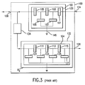
- the transmit FBAR array 102 is composed of a series of FBARs 101, 103, 105 and shunt FBARs 107, 109 connected to form a ladder circuit.
- the series FBARs are connected in series between the transmit port and the antenna port, the shunt FBAR 107 is connected between ground and the node between the series FBARs 101, 103 and the shunt FBAR 109 is connected between ground and the node between the series FBARs 103, 105.
- Figure 3 illustrates a 2 1 ⁇ 2- stage ladder circuit.
- the transmit FBAR array may include any number of full stages, each composed of one series FBAR and one shunt FBAR.
- the number of 1 ⁇ 2 stages depends upon the desire filter characteristics of the transmit band-pass filter and the characteristics of the individual FBARS constituting the transmit FBAR array.
- the receive band-pass filter is required to attenuate the transmit signal at the antenna port to such a low level that the residual transmit signal mixed with the receive signal at the receive port does not overload the highly sensitive low noise amplifier of the receiver connected to the receive port. Consequently, the transmit signal rejection requirements of the receive band-pass filter are considerably more stringent that the receive signal rejections requirements of the transmit band-pass filter. To provide the desired filter characteristics for the receive band-pass filter, not all of the shunt FBARs in the receive FBAR array should have the same resonant frequency.
- the receive band-pass filter is composed of an integrated receive FBAR array, the series auxiliary inductors 241, 243 and the shunt auxiliary inductors 231, 233, 235, and 237. All the FBARs are manufactured on a common piezoelectric layer.
- the receive FBAR array is composed of the series FBARs 211, 213, and 215 and the shunt FBARs 221, 223, 225, and 227 connected to form a ladder circuit.
- the series auxiliary inductor 241, the series FBARs, and the series auxiliary inductor are connected in series between the end of the 90° phase shifter remote from the antenna port and the receive port.
- the shunt FBAR 221 and the shunt auxiliary inductor 231 are connected in series between ground and the node between the series auxiliary inductor 241 and the series FBAR 211.
- the shunt FBAR 223 and the shunt auxiliary inductor 233 are connected in series between ground and the node between the series FBARS 211 and 213.
- the shunt FBAR 225 and the shunt auxiliary inductor 235 are connected in series between ground and the node between the series FBARs 213 and 215.
- the shunt FBAR 227 and the shunt auxiliary inductor 237 are connected in series between ground and the node between the series FBAR 215 and the series auxiliary inductor 243.
- Figure 5 illustrates a 31 ⁇ 2 stage ladder circuit. The number of full stages and the number of half stages depends upon the desired filter characteristics of the receive band pass filter and the characteristics of the individual FBARs constituting the receive FBAR array.
- Each auxiliary inductance has two main effects, mainly to slightly reduce the frequency of the series resonance of the corresponding FBAR, and to introduce an additional series resonance.
- the auxiliary inductance has a negligible effect on the frequency of the parallel resonance. Hence, each auxiliary inductor "tunes" the corresponding FBAR.
- a filter assembly includes a receive band filter chip having FBARs attached to a ceramic substrate through a die attach paddle. Wire-bonds extend from the chip to wire-bond pads positioned on the ceramic substrate. A die-attach paddle is electrically connected to a ground plane within the ceramic substrate.
- the victimizer loop shown as a dashed line in the 4 stage receive-band filter illustrated in Figure 4, carries a large amount of current from the filter chip input (pin 2) to ground.
- the victim loop shown as a dotted line, preferably carries a small amount of current from the filter chip output (pin 3) to ground.
- the victim loop is susceptible to magnetic fields over time.
- the victimizer loop can induce parasitic current in the victim loop.
- the area of either current loop may be minimized. However, optimum results are achieved when the areas of both current loops are minimized.
- the current loops are placed as close as possible to the ground plane. As shown in Figure 4, the area of the victim and victimizer loops are minimized and the loops are placed as far apart as possible in the package.
- the wirebonds of the pair of pins 1 and 3 and the pair of pins 2 and 4 are perpendicular to each other for maximum isolation.
- the loops should be as far apart as possible to minimize coupling. For pin isolation, the distance between the "victim" pin and the victimizer pins should be maximized.
- the parasitic current may be further controlled by the layout of the victimizer loop.
- the receiver band filter chip is preferably laid out such that the two shunts farthest apart in the filter are physically the farthest apart. Ideally, all the pins are far apart, but it is most critical that pins 1 and 4 are the farthest apart. Next in importance are pins 1 and 3 and pins 2 and 4. The remaining combinations are not as important.
- the mutual inductance between pins is roughly proportional to the square of the height of the chip, wire-bonds, and package pins to the grounded die-attach metal paddle, this height should be minimized. Furthermore, the ground inductance of the metal paddle should be minimized. The mutual inductance between the two leads connecting the chip to the PCB can be minimized when there is a short wire bond to the die-attach paddle.
Landscapes
- Physics & Mathematics (AREA)
- Acoustics & Sound (AREA)
- Piezo-Electric Or Mechanical Vibrators, Or Delay Or Filter Circuits (AREA)
- Surface Acoustic Wave Elements And Circuit Networks Thereof (AREA)
- Transceivers (AREA)
Applications Claiming Priority (2)
| Application Number | Priority Date | Filing Date | Title |
|---|---|---|---|
| US70249900A | 2000-10-31 | 2000-10-31 | |
| US702499 | 2000-10-31 |
Publications (2)
| Publication Number | Publication Date |
|---|---|
| EP1202455A2 true EP1202455A2 (de) | 2002-05-02 |
| EP1202455A3 EP1202455A3 (de) | 2004-09-15 |
Family
ID=24821459
Family Applications (1)
| Application Number | Title | Priority Date | Filing Date |
|---|---|---|---|
| EP01113271A Withdrawn EP1202455A3 (de) | 2000-10-31 | 2001-05-31 | Verfahren zum Verpacken von Duplexern unter Gebrauch von akustischen Dünnfilmvolumenresonatoren |
Country Status (3)
| Country | Link |
|---|---|
| US (1) | US6838956B2 (de) |
| EP (1) | EP1202455A3 (de) |
| JP (1) | JP2002198848A (de) |
Cited By (1)
| Publication number | Priority date | Publication date | Assignee | Title |
|---|---|---|---|---|
| US7414496B2 (en) | 2004-10-08 | 2008-08-19 | Infineon Technologies Ag | Filter structure and method for the design of a filter |
Families Citing this family (39)
| Publication number | Priority date | Publication date | Assignee | Title |
|---|---|---|---|---|
| US7030718B1 (en) * | 2002-08-09 | 2006-04-18 | National Semiconductor Corporation | Apparatus and method for extending tuning range of electro-acoustic film resonators |
| KR100486627B1 (ko) * | 2003-02-21 | 2005-05-03 | 엘지전자 주식회사 | 반도체 패키지 |
| US7275292B2 (en) * | 2003-03-07 | 2007-10-02 | Avago Technologies Wireless Ip (Singapore) Pte. Ltd. | Method for fabricating an acoustical resonator on a substrate |
| KR100616511B1 (ko) * | 2003-09-24 | 2006-08-29 | 삼성전기주식회사 | Fbar 소자 및 그 제조 방법 |
| JP2005159896A (ja) * | 2003-11-27 | 2005-06-16 | Sanyo Electric Co Ltd | アンテナ共用器 |
| US7615833B2 (en) | 2004-07-13 | 2009-11-10 | Avago Technologies Wireless Ip (Singapore) Pte. Ltd. | Film bulk acoustic resonator package and method of fabricating same |
| US7388454B2 (en) * | 2004-10-01 | 2008-06-17 | Avago Technologies Wireless Ip Pte Ltd | Acoustic resonator performance enhancement using alternating frame structure |
| US8981876B2 (en) | 2004-11-15 | 2015-03-17 | Avago Technologies General Ip (Singapore) Pte. Ltd. | Piezoelectric resonator structures and electrical filters having frame elements |
| US7202560B2 (en) | 2004-12-15 | 2007-04-10 | Avago Technologies Wireless Ip (Singapore) Pte. Ltd. | Wafer bonding of micro-electro mechanical systems to active circuitry |
| US7791434B2 (en) * | 2004-12-22 | 2010-09-07 | Avago Technologies Wireless Ip (Singapore) Pte. Ltd. | Acoustic resonator performance enhancement using selective metal etch and having a trench in the piezoelectric |
| US7369013B2 (en) * | 2005-04-06 | 2008-05-06 | Avago Technologies Wireless Ip Pte Ltd | Acoustic resonator performance enhancement using filled recessed region |
| US7443269B2 (en) * | 2005-07-27 | 2008-10-28 | Avago Technologies General Ip (Singapore) Pte. Ltd. | Method and apparatus for selectively blocking radio frequency (RF) signals in a radio frequency (RF) switching circuit |
| JP3115597U (ja) * | 2005-08-09 | 2005-11-10 | Uro電子工業株式会社 | 面実装用トランス |
| US7737807B2 (en) * | 2005-10-18 | 2010-06-15 | Avago Technologies Wireless Ip (Singapore) Pte. Ltd. | Acoustic galvanic isolator incorporating series-connected decoupled stacked bulk acoustic resonators |
| US20070210724A1 (en) * | 2006-03-09 | 2007-09-13 | Mark Unkrich | Power adapter and DC-DC converter having acoustic transformer |
| US20070210748A1 (en) * | 2006-03-09 | 2007-09-13 | Mark Unkrich | Power supply and electronic device having integrated power supply |
| US7746677B2 (en) * | 2006-03-09 | 2010-06-29 | Avago Technologies Wireless Ip (Singapore) Pte. Ltd. | AC-DC converter circuit and power supply |
| US7479685B2 (en) * | 2006-03-10 | 2009-01-20 | Avago Technologies General Ip (Singapore) Pte. Ltd. | Electronic device on substrate with cavity and mitigated parasitic leakage path |
| US7855618B2 (en) * | 2008-04-30 | 2010-12-21 | Avago Technologies Wireless Ip (Singapore) Pte. Ltd. | Bulk acoustic resonator electrical impedance transformers |
| US7732977B2 (en) * | 2008-04-30 | 2010-06-08 | Avago Technologies Wireless Ip (Singapore) | Transceiver circuit for film bulk acoustic resonator (FBAR) transducers |
| US8902023B2 (en) * | 2009-06-24 | 2014-12-02 | Avago Technologies General Ip (Singapore) Pte. Ltd. | Acoustic resonator structure having an electrode with a cantilevered portion |
| US8248185B2 (en) * | 2009-06-24 | 2012-08-21 | Avago Technologies Wireless Ip (Singapore) Pte. Ltd. | Acoustic resonator structure comprising a bridge |
| DE102009034101B4 (de) * | 2009-07-21 | 2017-02-02 | Epcos Ag | Filterschaltung mit verbesserter Filtercharakteristik |
| US8193877B2 (en) * | 2009-11-30 | 2012-06-05 | Avago Technologies Wireless Ip (Singapore) Pte. Ltd. | Duplexer with negative phase shifting circuit |
| US9243316B2 (en) | 2010-01-22 | 2016-01-26 | Avago Technologies General Ip (Singapore) Pte. Ltd. | Method of fabricating piezoelectric material with selected c-axis orientation |
| US8796904B2 (en) | 2011-10-31 | 2014-08-05 | Avago Technologies General Ip (Singapore) Pte. Ltd. | Bulk acoustic resonator comprising piezoelectric layer and inverse piezoelectric layer |
| US8962443B2 (en) | 2011-01-31 | 2015-02-24 | Avago Technologies General Ip (Singapore) Pte. Ltd. | Semiconductor device having an airbridge and method of fabricating the same |
| US9048812B2 (en) | 2011-02-28 | 2015-06-02 | Avago Technologies General Ip (Singapore) Pte. Ltd. | Bulk acoustic wave resonator comprising bridge formed within piezoelectric layer |
| US9083302B2 (en) | 2011-02-28 | 2015-07-14 | Avago Technologies General Ip (Singapore) Pte. Ltd. | Stacked bulk acoustic resonator comprising a bridge and an acoustic reflector along a perimeter of the resonator |
| US9425764B2 (en) | 2012-10-25 | 2016-08-23 | Avago Technologies General Ip (Singapore) Pte. Ltd. | Accoustic resonator having composite electrodes with integrated lateral features |
| US9203374B2 (en) | 2011-02-28 | 2015-12-01 | Avago Technologies General Ip (Singapore) Pte. Ltd. | Film bulk acoustic resonator comprising a bridge |
| US9154112B2 (en) | 2011-02-28 | 2015-10-06 | Avago Technologies General Ip (Singapore) Pte. Ltd. | Coupled resonator filter comprising a bridge |
| US9148117B2 (en) | 2011-02-28 | 2015-09-29 | Avago Technologies General Ip (Singapore) Pte. Ltd. | Coupled resonator filter comprising a bridge and frame elements |
| US9136818B2 (en) | 2011-02-28 | 2015-09-15 | Avago Technologies General Ip (Singapore) Pte. Ltd. | Stacked acoustic resonator comprising a bridge |
| US9444426B2 (en) | 2012-10-25 | 2016-09-13 | Avago Technologies General Ip (Singapore) Pte. Ltd. | Accoustic resonator having integrated lateral feature and temperature compensation feature |
| US8575820B2 (en) | 2011-03-29 | 2013-11-05 | Avago Technologies General Ip (Singapore) Pte. Ltd. | Stacked bulk acoustic resonator |
| US8350445B1 (en) | 2011-06-16 | 2013-01-08 | Avago Technologies Wireless Ip (Singapore) Pte. Ltd. | Bulk acoustic resonator comprising non-piezoelectric layer and bridge |
| US8922302B2 (en) | 2011-08-24 | 2014-12-30 | Avago Technologies General Ip (Singapore) Pte. Ltd. | Acoustic resonator formed on a pedestal |
| US9236997B2 (en) * | 2013-09-23 | 2016-01-12 | Broadcom Corporation | Wireless transceiver with circulator-based quadrature duplexer and methods for use therewith |
Family Cites Families (6)
| Publication number | Priority date | Publication date | Assignee | Title |
|---|---|---|---|---|
| US4112147A (en) * | 1977-05-13 | 1978-09-05 | Western Electric Company, Inc. | Method of manufacturing a monolithic crystal filter |
| US5162822A (en) * | 1988-10-31 | 1992-11-10 | Hitachi, Ltd. | Saw filter chip mounted on a substrate with shielded conductors on opposite surfaces |
| TW438155U (en) * | 1995-07-27 | 2001-05-28 | Daishinku Corp | Multi-mode piezoelectric filter |
| JPH10178327A (ja) * | 1996-12-19 | 1998-06-30 | Toshiba Corp | 弾性表面波装置 |
| US6262637B1 (en) * | 1999-06-02 | 2001-07-17 | Agilent Technologies, Inc. | Duplexer incorporating thin-film bulk acoustic resonators (FBARs) |
| US6377137B1 (en) * | 2000-09-11 | 2002-04-23 | Agilent Technologies, Inc. | Acoustic resonator filter with reduced electromagnetic influence due to die substrate thickness |
-
2001
- 2001-05-31 EP EP01113271A patent/EP1202455A3/de not_active Withdrawn
- 2001-10-31 JP JP2001334685A patent/JP2002198848A/ja not_active Ceased
-
2002
- 2002-09-13 US US10/243,144 patent/US6838956B2/en not_active Expired - Fee Related
Cited By (1)
| Publication number | Priority date | Publication date | Assignee | Title |
|---|---|---|---|---|
| US7414496B2 (en) | 2004-10-08 | 2008-08-19 | Infineon Technologies Ag | Filter structure and method for the design of a filter |
Also Published As
| Publication number | Publication date |
|---|---|
| JP2002198848A (ja) | 2002-07-12 |
| EP1202455A3 (de) | 2004-09-15 |
| US20030011446A1 (en) | 2003-01-16 |
| US6838956B2 (en) | 2005-01-04 |
Similar Documents
| Publication | Publication Date | Title |
|---|---|---|
| EP1202455A2 (de) | Verfahren zum Verpacken von Duplexern unter Gebrauch von akustischen Dünnfilmvolumenresonatoren | |
| US7339445B2 (en) | BAW duplexer without phase shifter | |
| CN100536352C (zh) | 用于减小便携式通信设备中接收损耗的方法、接收前端模块和便携式通信设备 | |
| US7035602B2 (en) | High-frequency composite switch component | |
| EP2362545A1 (de) | Filter, duplexer und elektronische anordnung | |
| EP1078414B1 (de) | Antennenschalter | |
| US6943645B2 (en) | Surface acoustic wave duplexer and communication apparatus having the same | |
| US8081047B2 (en) | Multi-band circuit with first and second signal branches | |
| US7167688B2 (en) | RF transceiver module formed in multi-layered ceramic | |
| US7756488B2 (en) | High-frequency switch module | |
| US20190273521A1 (en) | Radio-frequency module and communication apparatus | |
| CN213213456U (zh) | 高频模块和通信装置 | |
| US20030092397A1 (en) | Diplexer, and high-frequency switch and antenna duplexer using the same | |
| US8620244B2 (en) | Electrical component with a front-end circuit | |
| US7454178B2 (en) | Low-loss transmitter module | |
| WO2006130969A1 (en) | Device and methods for high isolation and interference suppression switch-filter | |
| CN214380892U (zh) | 高频模块和通信装置 | |
| US20050073375A1 (en) | Single chip-type film bulk acoustic resonator duplexer | |
| US20070159274A1 (en) | SAW filter and portable terminal | |
| US20130309985A1 (en) | Transmission module | |
| CN213213457U (zh) | 高频模块和通信装置 | |
| US6765456B2 (en) | Surface acoustic wave duplexer and portable communication device using the same | |
| JP3851184B2 (ja) | フロントエンドモジュール | |
| CN1774858B (zh) | 改善隔离的双波段功率放大器 | |
| US20230179157A1 (en) | High-frequency circuit and communication device |
Legal Events
| Date | Code | Title | Description |
|---|---|---|---|
| PUAI | Public reference made under article 153(3) epc to a published international application that has entered the european phase |
Free format text: ORIGINAL CODE: 0009012 |
|
| AK | Designated contracting states |
Kind code of ref document: A2 Designated state(s): AT BE CH CY DE DK ES FI FR GB GR IE IT LI LU MC NL PT SE TR |
|
| AX | Request for extension of the european patent |
Free format text: AL;LT;LV;MK;RO;SI |
|
| PUAL | Search report despatched |
Free format text: ORIGINAL CODE: 0009013 |
|
| AK | Designated contracting states |
Kind code of ref document: A3 Designated state(s): AT BE CH CY DE DK ES FI FR GB GR IE IT LI LU MC NL PT SE TR |
|
| AX | Request for extension of the european patent |
Extension state: AL LT LV MK RO SI |
|
| 17P | Request for examination filed |
Effective date: 20041029 |
|
| AKX | Designation fees paid |
Designated state(s): DE FR GB IT |
|
| RAP1 | Party data changed (applicant data changed or rights of an application transferred) |
Owner name: AVAGO TECHNOLOGIES WIRELESS IP (SINGAPORE) PTE. LT |
|
| 17Q | First examination report despatched |
Effective date: 20070213 |
|
| STAA | Information on the status of an ep patent application or granted ep patent |
Free format text: STATUS: THE APPLICATION IS DEEMED TO BE WITHDRAWN |
|
| 18D | Application deemed to be withdrawn |
Effective date: 20070824 |