EP1205304A1 - Imprimante, tête d'impression et son procédé de fabrication - Google Patents
Imprimante, tête d'impression et son procédé de fabrication Download PDFInfo
- Publication number
- EP1205304A1 EP1205304A1 EP01126305A EP01126305A EP1205304A1 EP 1205304 A1 EP1205304 A1 EP 1205304A1 EP 01126305 A EP01126305 A EP 01126305A EP 01126305 A EP01126305 A EP 01126305A EP 1205304 A1 EP1205304 A1 EP 1205304A1
- Authority
- EP
- European Patent Office
- Prior art keywords
- ink
- wiring pattern
- ink chamber
- partition
- heating element
- Prior art date
- Legal status (The legal status is an assumption and is not a legal conclusion. Google has not performed a legal analysis and makes no representation as to the accuracy of the status listed.)
- Granted
Links
Images



Classifications
-
- B—PERFORMING OPERATIONS; TRANSPORTING
- B41—PRINTING; LINING MACHINES; TYPEWRITERS; STAMPS
- B41J—TYPEWRITERS; SELECTIVE PRINTING MECHANISMS, i.e. MECHANISMS PRINTING OTHERWISE THAN FROM A FORME; CORRECTION OF TYPOGRAPHICAL ERRORS
- B41J2/00—Typewriters or selective printing mechanisms characterised by the printing or marking process for which they are designed
- B41J2/005—Typewriters or selective printing mechanisms characterised by the printing or marking process for which they are designed characterised by bringing liquid or particles selectively into contact with a printing material
- B41J2/01—Ink jet
- B41J2/135—Nozzles
- B41J2/16—Production of nozzles
- B41J2/1621—Manufacturing processes
- B41J2/164—Manufacturing processes thin film formation
- B41J2/1646—Manufacturing processes thin film formation thin film formation by sputtering
-
- B—PERFORMING OPERATIONS; TRANSPORTING
- B41—PRINTING; LINING MACHINES; TYPEWRITERS; STAMPS
- B41J—TYPEWRITERS; SELECTIVE PRINTING MECHANISMS, i.e. MECHANISMS PRINTING OTHERWISE THAN FROM A FORME; CORRECTION OF TYPOGRAPHICAL ERRORS
- B41J2/00—Typewriters or selective printing mechanisms characterised by the printing or marking process for which they are designed
- B41J2/005—Typewriters or selective printing mechanisms characterised by the printing or marking process for which they are designed characterised by bringing liquid or particles selectively into contact with a printing material
- B41J2/01—Ink jet
- B41J2/135—Nozzles
- B41J2/14—Structure thereof only for on-demand ink jet heads
- B41J2/14016—Structure of bubble jet print heads
- B41J2/14072—Electrical connections, e.g. details on electrodes, connecting the chip to the outside...
-
- B—PERFORMING OPERATIONS; TRANSPORTING
- B41—PRINTING; LINING MACHINES; TYPEWRITERS; STAMPS
- B41J—TYPEWRITERS; SELECTIVE PRINTING MECHANISMS, i.e. MECHANISMS PRINTING OTHERWISE THAN FROM A FORME; CORRECTION OF TYPOGRAPHICAL ERRORS
- B41J2/00—Typewriters or selective printing mechanisms characterised by the printing or marking process for which they are designed
- B41J2/005—Typewriters or selective printing mechanisms characterised by the printing or marking process for which they are designed characterised by bringing liquid or particles selectively into contact with a printing material
- B41J2/01—Ink jet
- B41J2/135—Nozzles
- B41J2/14—Structure thereof only for on-demand ink jet heads
- B41J2/14016—Structure of bubble jet print heads
- B41J2/14088—Structure of heating means
- B41J2/14112—Resistive element
- B41J2/14129—Layer structure
-
- B—PERFORMING OPERATIONS; TRANSPORTING
- B41—PRINTING; LINING MACHINES; TYPEWRITERS; STAMPS
- B41J—TYPEWRITERS; SELECTIVE PRINTING MECHANISMS, i.e. MECHANISMS PRINTING OTHERWISE THAN FROM A FORME; CORRECTION OF TYPOGRAPHICAL ERRORS
- B41J2/00—Typewriters or selective printing mechanisms characterised by the printing or marking process for which they are designed
- B41J2/005—Typewriters or selective printing mechanisms characterised by the printing or marking process for which they are designed characterised by bringing liquid or particles selectively into contact with a printing material
- B41J2/01—Ink jet
- B41J2/135—Nozzles
- B41J2/16—Production of nozzles
- B41J2/1601—Production of bubble jet print heads
- B41J2/1603—Production of bubble jet print heads of the front shooter type
-
- B—PERFORMING OPERATIONS; TRANSPORTING
- B41—PRINTING; LINING MACHINES; TYPEWRITERS; STAMPS
- B41J—TYPEWRITERS; SELECTIVE PRINTING MECHANISMS, i.e. MECHANISMS PRINTING OTHERWISE THAN FROM A FORME; CORRECTION OF TYPOGRAPHICAL ERRORS
- B41J2/00—Typewriters or selective printing mechanisms characterised by the printing or marking process for which they are designed
- B41J2/005—Typewriters or selective printing mechanisms characterised by the printing or marking process for which they are designed characterised by bringing liquid or particles selectively into contact with a printing material
- B41J2/01—Ink jet
- B41J2/135—Nozzles
- B41J2/16—Production of nozzles
- B41J2/1621—Manufacturing processes
- B41J2/1623—Manufacturing processes bonding and adhesion
-
- B—PERFORMING OPERATIONS; TRANSPORTING
- B41—PRINTING; LINING MACHINES; TYPEWRITERS; STAMPS
- B41J—TYPEWRITERS; SELECTIVE PRINTING MECHANISMS, i.e. MECHANISMS PRINTING OTHERWISE THAN FROM A FORME; CORRECTION OF TYPOGRAPHICAL ERRORS
- B41J2/00—Typewriters or selective printing mechanisms characterised by the printing or marking process for which they are designed
- B41J2/005—Typewriters or selective printing mechanisms characterised by the printing or marking process for which they are designed characterised by bringing liquid or particles selectively into contact with a printing material
- B41J2/01—Ink jet
- B41J2/135—Nozzles
- B41J2/16—Production of nozzles
- B41J2/1621—Manufacturing processes
- B41J2/1626—Manufacturing processes etching
- B41J2/1628—Manufacturing processes etching dry etching
-
- B—PERFORMING OPERATIONS; TRANSPORTING
- B41—PRINTING; LINING MACHINES; TYPEWRITERS; STAMPS
- B41J—TYPEWRITERS; SELECTIVE PRINTING MECHANISMS, i.e. MECHANISMS PRINTING OTHERWISE THAN FROM A FORME; CORRECTION OF TYPOGRAPHICAL ERRORS
- B41J2/00—Typewriters or selective printing mechanisms characterised by the printing or marking process for which they are designed
- B41J2/005—Typewriters or selective printing mechanisms characterised by the printing or marking process for which they are designed characterised by bringing liquid or particles selectively into contact with a printing material
- B41J2/01—Ink jet
- B41J2/135—Nozzles
- B41J2/16—Production of nozzles
- B41J2/1621—Manufacturing processes
- B41J2/1631—Manufacturing processes photolithography
-
- B—PERFORMING OPERATIONS; TRANSPORTING
- B41—PRINTING; LINING MACHINES; TYPEWRITERS; STAMPS
- B41J—TYPEWRITERS; SELECTIVE PRINTING MECHANISMS, i.e. MECHANISMS PRINTING OTHERWISE THAN FROM A FORME; CORRECTION OF TYPOGRAPHICAL ERRORS
- B41J2/00—Typewriters or selective printing mechanisms characterised by the printing or marking process for which they are designed
- B41J2/005—Typewriters or selective printing mechanisms characterised by the printing or marking process for which they are designed characterised by bringing liquid or particles selectively into contact with a printing material
- B41J2/01—Ink jet
- B41J2/135—Nozzles
- B41J2/16—Production of nozzles
- B41J2/1621—Manufacturing processes
- B41J2/164—Manufacturing processes thin film formation
- B41J2/1642—Manufacturing processes thin film formation thin film formation by CVD [chemical vapor deposition]
-
- B—PERFORMING OPERATIONS; TRANSPORTING
- B41—PRINTING; LINING MACHINES; TYPEWRITERS; STAMPS
- B41J—TYPEWRITERS; SELECTIVE PRINTING MECHANISMS, i.e. MECHANISMS PRINTING OTHERWISE THAN FROM A FORME; CORRECTION OF TYPOGRAPHICAL ERRORS
- B41J2202/00—Embodiments of or processes related to ink-jet or thermal heads
- B41J2202/01—Embodiments of or processes related to ink-jet heads
- B41J2202/13—Heads having an integrated circuit
Definitions
- the present invention relates to a printer, a printer head, and a method of producing the printer head.
- the present invention is applicable to a printer which makes use of a process which causes ink droplets to fly out as a result of heating by a heater.
- the present invention makes it possible to, by preventing a thickness-direction stepped portion from being formed at at least a partition of an ink chamber as a result of disposing a wiring pattern below the partition of the ink chamber, bring an orifice plate sufficiently into close contact with what it is to be bonded to and bond it thereto.
- a dot is formed by causing small drops of recording liquid (ink) to fly out from a nozzle of a recording head and causing them to adhere to what is to be subjected to a recording operation.
- the inkjet process is classified into, for example, an electrostatic attraction process, a continuous vibration generation process (piezo process), and a thermal process, depending on the method used to cause the ink to fly out.
- air bubbles are produced by heating localized portions of the ink in order to push out the ink from a discharge opening by the air bubbles, thereby causing the ink to fly out to what is to be subjected to printing. This makes it possible to print a color image using a simple structure.
- a printer which operates by this thermal process is constructed using what is called a printer head, which has mounted therein a heating element which heats ink, a drive circuit based on a logic integrated circuit which drives the heating element, and other component parts.
- Fig. 8 is a sectional view partly showing a thermal head.
- an isolation area 3 LOCOS: local oxidation of silicon
- MOS metal oxide semiconductor
- a contact hole is formed in order to form a first-layer wiring pattern 7.
- the MOS transistors 5 and 6, forming the drive circuit are connected to each other, thereby forming a logic integrated circuit.
- heating element materials such as tantalum, tantalum aluminum, or titanium nitride
- heating elements 8 which heat ink are formed.
- a contact hole is formed to form a second-layer wiring pattern 9.
- a connection portion between the switching transistors 4 and the heating elements 8 a connection portion between the heating elements 8 and a power supply, a ground line, and the like, are formed.
- an insulating material such as SiO 2 or SiN, is deposited in order to form a protective layer 10, after which a Ta film is formed on localized portions of the heating elements 8.
- a cavitation resistance layer 11 is formed.
- a dry film 13 and an orifice plate 14 are successively placed upon each other.
- the dry film 13 is formed of, for example, carbon resin. After placing it by contact bonding, portions thereof situated in correspondence with an ink chamber and an ink path are removed, after which a hardening operation is carried out.
- the orifice plate 14 is formed of a plate-shaped material which is processed into a predetermined shape so that a nozzle 15, which is a very small ink discharge opening, is formed above the heating elements 8.
- the orifice plate 14 is supported on the top portion of the dry film 13 as a result of adhering it thereto.
- the nozzle 15, an ink chamber 16, a path for guiding ink into the ink chamber 16, etc. are formed at the printer head 1.
- the ink is guided to the ink chamber 16, and, by a switching operation of the switching transistors 4, the heating elements 8 generate heat in order to heat localized portions of the ink.
- the heating core air bubbles are produced at side surfaces of the heating elements 8 of the ink chamber 16. These core air bubbles combine to form film air bubbles.
- pressure is increased by the air bubbles, the ink is pushed out from the nozzle 15 and flies out to what is to be subjected to printing.
- intermittent heating by the heating elements 8 causes the ink to successively adhere to what is to be subjected to printing, so that a desired image is formed.
- the switching transistors 4, which drive the heating elements 8 are controlled by the same logic integrated circuit formed by the MOS transistors 5 and 6. Therefore, the heating elements 8 are disposed very closely together, thereby making it possible to reliably drive them by their corresponding switching transistors.
- the heating elements 8 need to be disposed very close to each other. More specifically, in order to obtain, for example, a 600 DPI printed result, the heating elements 8 need to be disposed at intervals of 42,333 ⁇ m. It is extremely difficult to dispose individual drive elements at the heating elements 8 disposed very close to each other. Therefore, in the printer head 1, for example, switching transistors are formed on the semiconductor substrate and are connected to the corresponding heating elements 8 by an integrated circuit technology. Then, by the drive circuits similarly formed on the semiconductor substrate, the corresponding switching transistors are driven in order to make it possible to simply and reliably drive each of the heating elements 8.
- the printer head 1 having such a structure has a problem in that it is difficult to bring the orifice plate 14 sufficiently into close contact with the dry film 13 and to bond it thereto.
- the first-layer wiring pattern 7 is formed with the minimum thickness required, and the second-layer wiring pattern 9, which forms a power supply line and a ground line, is made thick in order to obtain a desired current capacity.
- the printer head 1 In contrast to this, in the printer head 1, the situation is reversed with respect to the case of the commonly used semiconductor integrated circuit, so that the first-layer wiring pattern is made thick, whereas the second-layer wiring pattern is made thin, in order to obtain good covering property at the silicon nitride film forming the ink protective layer 10 and the tantalum cavitation resistance layer 11, which are formed above the heating elements 8.
- the second-layer wiring pattern is formed with a thickness of the order of 1 ⁇ m when an aluminum wiring pattern is used, and a stepped portion having a size of the order of 1 ⁇ m is formed at the second-layer wiring pattern 9.
- the stepped portion having a size of the order of 1 ⁇ m is formed at the second-layer wiring pattern 9
- very fine recesses and protrusions are formed at the surface of the protective layer 10, which is formed on top of the wiring pattern 9, and the surface of the dry film 13. Because of the very fine recesses and protrusions, it becomes difficult to bring the orifice plate 14 sufficiently into close contact with the dry film 13 and to bond it thereto. In this connection, when the surfaces of the protective layer 10 and the dry film 13 become very uneven, ink leakage may occur.
- Fig. 9A is a plan view of the printer head 1 in which the dry film 13 has been removed
- Fig. 9B is a sectional view of the printer head 1, with the sectional view being formed by cutting a plane at a base-side partition of the ink chamber in a direction perpendicular to the illustration shown in Fig. 8.
- a gap is correspondingly produced between the dry film 13 and the orifice plate 14. The gap may cause ink to leak from the partition of the ink chamber.
- Fig. 9A is a plan view of the printer head 1 in which the dry film 13 has been removed
- Fig. 9B is a sectional view of the printer head 1, with the sectional view being formed by cutting a plane at a base-side partition of the ink chamber in a direction perpendicular to the illustration shown in Fig. 8.
- the wiring pattern 9 is not disposed at all at the partition of the ink chamber beside it, so that the area of the gap becomes large, thereby causing the ink leakage to become noticeable at this portion.
- the structure shown in Figs. 9A and 9B is a type in which ink is supplied from an edge of the semiconductor substrate.
- the lamination materials other than the second-layer wiring pattern 9 are not shown, and the external shape of the dry film 13 is shown by dotted lines.
- the present invention is applied to the printer, the printer head, or the method of producing the printer head, and, by disposing a wiring pattern below a partition of an ink chamber, a thickness-direction stepped portion is prevented from being formed at at least the partition of the ink chamber.
- the structure of the present invention by preventing a thickness-direction stepped portion from being formed at at least the partition of the ink chamber by disposing a wiring pattern below the partition of the ink chamber, it is possible to, by using a simple structure, prevent formation of a gap between a material forming the partition of the ink chamber and a plate-shaped material, which is an orifice plate, disposed above the material forming the partition of the ink chamber. This makes it possible to prevent ink leakage, so that the orifice plate can be bonded by bringing it sufficiently into close contact with what it is to be bonded to.
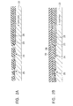
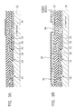
- Figs. 2A to 4 are sectional views illustrating the steps of producing a printer head of an embodiment of the present invention.
- silicon nitride films are deposited thereon.
- the silicon substrate 22 is processed in order to remove the silicon nitride films deposited on areas other than predetermined areas where transistors are formed.
- silicon nitride films are formed in the areas on the silicon substrate 22 where the transistors are to be formed.
- thermal silicon oxide films are formed in the areas from which the silicon nitride films have been removed, and, by the thermal silicon oxide films, an isolation area (LOCOS) 23 for isolating the transistors is formed.
- LOC isolation area
- gates having tungsten silicide/polysilicon/thermally oxide film structures are formed.
- the silicon substrate 22 is processed in order to form, for example, MOS switching transistors 24 and 25.
- the switching transistor 24 is a MOS driver transistor having a pressure resistance of the order of 30 V, and is used to drive heating elements.
- the transistor 25 forms an integrated circuit that controls the driver transistor, and operates by a voltage of 5 V. Then, in the process, by CVD (chemical vapor deposition), a BPSG (borophosepho silicate glass) film 26 is deposited in order to form an interlayer insulating film.
- CVD chemical vapor deposition
- connection hole is formed at a silicon semiconductor diffusion layer (source ⁇ drain).
- first-layer wiring pattern 28 the MOS transistor 25, forming a drive circuit, is connected in order to form a logic integrated circuit.
- a silicon oxide film 29 (what is called TEOS), which is an interlayer insulating film, is deposited by CVD in order to, by CMP (chemical mechanical polishing) or resist etch back, smoothen the silicon oxide film 29.
- a titanium film having a film thickness of 10 nm is deposited as a close contact layer.
- titanium nitride or tantalum is deposited to a film thickness of 100 nm, so that resistance films are deposited on the semiconductor substrate 22.
- heating elements 30 are formed so as to have substantially square shapes.
- a silicon nitride film 31 having a film thickness of 300 nm is deposited.
- a connection hole (via hole) following the formation of the first-layer wiring pattern 28 is formed.
- titanium, titanium nitride barrier metal, and aluminum to which 0.5at% of copper has been added are successively deposited to film thicknesses of 20 ⁇ m, 50 ⁇ m, and 100 nm, respectively.
- second-layer wiring patterns 32 are formed.
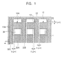
- the second-layer wiring patterns 32 power supply wiring patterns and ground wiring patterns are formed, and a wiring pattern for connecting the drive transistor 24 to the heating elements is formed, so that a thickness-direction stepped portion is not formed at a partition of each ink chamber.
- the printer head is constructed so that ink is supplied from an edge in a longitudinal direction.
- the partition of each ink chamber 16 is formed by a dry film 13 so as to be U-shaped in this plan view so that each ink chamber 16 opens to the ink-supply-side edge.
- each wiring pattern 32A which is connected to one end of its corresponding heating element 30, is disposed so that it crosses below the back partition of its corresponding ink chamber 16.
- Each wiring pattern 32B which is connected to the other end of its corresponding heating element 30, is disposed so that it extends along the ink-supply-side edge and is bent and extends below its corresponding ink chamber partition wall that extends at this edge side, so as to be substantially parallel to its corresponding wiring pattern 32A substantially due to the width of its corresponding partition.
- the pattern widths of the wiring patterns 32A are selected so that the distances between the pairs of wiring patterns 32A and 32B are approximately 5 ⁇ m at the portions where the pairs of wiring patterns 32A and 32B extend parallel to each other. Pattern widths are also selected so that adjacent ink chamber wiring patterns 32B are separated by about 5 ⁇ m so as to extend parallel to each other.
- the widths of the wiring patterns 32A and the wiring patterns 32B are selected so that the distances between the adjacent wiring patterns 32A and 32B become small, within a range which makes it possible to prevent accidents, such as short circuits. Therefore, it is possible prevent leakage of ink at the back side of each ink chamber 16. Consequently, as in the embodiment, when the wiring patterns 32A and 32B are separated by approximately 5 ⁇ m, a side surface of an orifice plate 14 at the dry film 13 can be formed into a substantially smooth surface, so that, at this portion, it is possible to prevent the leakage of ink.
- a partition 13A of the endmost ink chamber has a dummy wiring pattern 32C, which is not used in any way in driving the heating elements 30.
- the dummy wiring pattern 32C is separated by approximately 5 ⁇ m from the adjacent wiring pattern 32A, so that, by this separation, it extends below the corresponding ink chamber partition due to the width of the partition. Therefore, in the printer head 1, even at this end portion, it is possible to prevent the leakage of ink by preventing the formation of a stepped portion.
- the dummy wiring pattern 32C is formed so that its front end side extends towards the ink-supply-side edge, is bent, and extends in the direction in which the heating elements 30 are disposed in a row. At the portion of the dummy wiring pattern 32C extending in the direction in which the heating elements 30 are arranged in a row, there are portions that oppose their corresponding partitions. These portions are formed so as to protrude towards their corresponding opposing wiring patterns 32B.
- the protruding portions of the dummy wiring pattern 32C are formed so as to be separated by 5 ⁇ m from the corresponding opposing wiring patterns 32B. Therefore, in the printer head, the front end side of the partition of each ink chamber is formed so that it is possible to prevent leakage of ink even between adjacent ink chambers, thereby making it possible to prevent very small tilting of the orifice plate 14 towards the edge.
- the dummy wiring pattern 32C is disposed in this way, and is connected to the ground lines of the second-layer wiring patterns 32. Therefore, in the printer head, the dummy wiring pattern 32C, which is not used in any way in driving the heating elements 30, is formed so as to make it possible to prevent various failures caused by disposing it close to the wiring patterns 32A and 32B.
- a silicon oxide film 33 which functions as an ink protective layer, is deposited.
- a tantalum film having a film thickness of 200 nm to 300 nm is deposited.
- a cavitation resistance layer 34 is formed.
- the dry film 13 and the orifice plate 14 are successively deposited, and form the ink chambers 16, an ink path used to guide the ink to the ink chambers 16, and a nozzle 15.
- photosensitive resin is used for the dry film 13. After placing it by contact bonding, an exposure operation is carried out to remove portions thereof in correspondence with the locations of the ink chambers and the ink path in order to form the dry film 13.
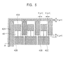
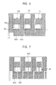
- Fig. 5 is a plan view of the structures of second-layer wiring patterns and heating elements in a second embodiment of a printer head of the present invention, shown in contrast to those shown in Fig. 1.
- the second-layer wiring patterns and the heating elements are formed by the layout shown in Fig. 5 instead of the above-described layout shown in Fig. 1.
- each heating element 40 ends of two resistance patterns that extend substantially parallel to each other are connected by a corresponding second-layer wiring pattern 42A, so that a folded-back shape is formed. Then, both ends of each of the heating elements 40 having folded-up shapes are connected to the power supply line and the switching transistor, respectively, by corresponding second-layer wiring patterns 42B and 42C.
- the wiring patterns 42B and the wiring patterns 42C are disposed sufficiently close to each other within a range not causing accidents, such as short circuits, and are disposed so as to cross below back partitions of the ink chambers. Therefore, also in the second embodiment, it possible to prevent the formation of stepped portions at the back sides of the ink chambers.
- the end-side wiring pattern 42B of the endmost heating element 40 is formed with a small width, so that, as in the first embodiment, a dummy wiring pattern 42D is disposed correspondingly.
- the wiring pattern 42D is formed so as to extend below the ink chamber partition at this end, and is disposed sufficiently close to the adjacent wiring pattern 42B within a range not causing accidents, such as short circuits. Therefore, it is possible to prevent the formation of a stepped portion at this end portion side.
- the dummy wiring pattern 42D is formed so that an end portion is bent at an edge side and extends along the edge.
- the dummy wiring pattern 42D is formed so that portions thereof protrude towards the back sides of the corresponding ink chambers, at the partitions of the corresponding ink chambers. Ends of the protruding portions are such as to oppose the corresponding wiring patterns 42A and 42B at a distance of approximately 5 ⁇ m. Therefore, the printer head is such as to make it possible to prevent leakage of ink between adjacent ink chambers.
- the dummy wiring pattern 42D is disposed in this way, and is connected to the ground lines of the second-layer wiring patterns. Therefore, in the printer head, it is possible to prevent various failures caused by disposing the dummy wiring pattern 42D, which is not used in any way in the driving of the heating elements 40, close to the wiring patterns 42A, 42B, and 42C.
- Fig. 6 is a plan view of the structures of second-layer wiring patterns and heating elements of a printer head of a third embodiment of the present invention, shown in contrast to those of Fig. 1.
- the printer head of the embodiment makes it possible to prevent leakage of liquid by preventing formation of a stepped portion as a result of extending wiring patterns 52A and 52B connected to heating elements 30.
- the wiring patterns 52B which are connected to edge-side end portions of the corresponding heating elements 30, are formed so that edge-side portions thereof below ink chamber partitions protrude towards an edge side. This makes it possible to prevent formation of stepped portions between adjacent ink chambers, so that ink leakage can be prevented from occurring.
- a connecting portion thereof which connects to the corresponding element 30 extends towards an end portion side and is bent, so that the endmost side wiring pattern extends below the partition of the ink chamber at this end portion side to a edge side. Therefore, in the embodiment, at this end portion side also, it is possible to prevent leakage of ink by preventing formation of a stepped portion.
- Fig. 7 is a plan view of the structures of second-layer wiring patterns and heating elements of a printer head of a fourth embodiment of the present invention, shown in contrast to those of Fig. 5.
- the printer head of the embodiment makes it possible to prevent leakage of liquid by preventing formation of stepped portions by extending wiring patterns 62A and 62B connected to heating elements 30.
- each wiring pattern 62B, connected to one end of its corresponding heating element 30, is formed so that a portion thereof disposed below its corresponding ink chamber partition is bent and extends below its corresponding ink chamber partition to an edge side. This makes it possible to prevent the leakage of ink by preventing formation of stepped portions between adjacent ink chambers.
- the endmost wiring pattern 62A is formed so that a connecting portion thereof that connects to the heating element 30 extends to an end portion side and is bent, so that the endmost wiring pattern 62A extends below the partition of the ink chamber at this end portion side to an edge side. Therefore, in this embodiment, at this end portion side also, it is possible to prevent leakage of ink by preventing formation of stepped portions.
- the present invention is not limited thereto, so that the present invention may be widely applied to, for example, a structure having one layer of wiring pattern or a structure having three of more layers of wiring patterns.
- the present invention is not limited thereto, so that the present invention may be widely applied to, for example, the case where the heating elements are disposed at the top side of the wiring pattern at the topmost layer.
- the present invention is not limited thereto, so various other types of lamination materials may be used when necessary.
Landscapes
- Engineering & Computer Science (AREA)
- Manufacturing & Machinery (AREA)
- Particle Formation And Scattering Control In Inkjet Printers (AREA)
Applications Claiming Priority (2)
| Application Number | Priority Date | Filing Date | Title |
|---|---|---|---|
| JP2000344233A JP4604337B2 (ja) | 2000-11-07 | 2000-11-07 | プリンタ、プリンタヘッド及びプリンタヘッドの製造方法 |
| JP2000344233 | 2000-11-07 |
Publications (2)
| Publication Number | Publication Date |
|---|---|
| EP1205304A1 true EP1205304A1 (fr) | 2002-05-15 |
| EP1205304B1 EP1205304B1 (fr) | 2009-10-14 |
Family
ID=18818462
Family Applications (1)
| Application Number | Title | Priority Date | Filing Date |
|---|---|---|---|
| EP01126305A Expired - Lifetime EP1205304B1 (fr) | 2000-11-07 | 2001-11-06 | Imprimante, tête d'impression et son procédé de fabrication |
Country Status (4)
| Country | Link |
|---|---|
| US (1) | US6592209B2 (fr) |
| EP (1) | EP1205304B1 (fr) |
| JP (1) | JP4604337B2 (fr) |
| DE (1) | DE60140167D1 (fr) |
Cited By (2)
| Publication number | Priority date | Publication date | Assignee | Title |
|---|---|---|---|---|
| EP1568498A3 (fr) * | 2004-02-25 | 2005-12-14 | Hewlett-Packard Development Company, L.P. | Disposition de couches métalliques d'un dispostif d'éjection de fluide |
| EP1567346A4 (fr) * | 2002-11-23 | 2008-07-23 | Silverbrook Res Pty Ltd | Tete d'impression par jet d'encre thermique dotee de dispositifs de rechauffement formes d'elements a faible numero atomique |
Families Citing this family (6)
| Publication number | Priority date | Publication date | Assignee | Title |
|---|---|---|---|---|
| JP4114202B2 (ja) | 2003-02-28 | 2008-07-09 | ソニー株式会社 | 液体吐出ヘッド、液体吐出装置及び液体吐出ヘッドの駆動方法 |
| JP5008448B2 (ja) * | 2007-04-20 | 2012-08-22 | キヤノン株式会社 | インクジェット記録ヘッド用の基板の製造方法 |
| JP5765924B2 (ja) * | 2010-12-09 | 2015-08-19 | キヤノン株式会社 | 液体吐出ヘッドの駆動方法、液体吐出ヘッド、及び液体吐出装置 |
| JP5350429B2 (ja) * | 2011-02-10 | 2013-11-27 | キヤノン株式会社 | インクジェット記録ヘッドの製造方法 |
| JP6011169B2 (ja) * | 2012-09-04 | 2016-10-19 | ブラザー工業株式会社 | 液滴吐出装置 |
| JP6746329B2 (ja) * | 2016-03-11 | 2020-08-26 | キヤノン株式会社 | 記録素子基板の製造方法及び液体吐出ヘッド |
Citations (3)
| Publication number | Priority date | Publication date | Assignee | Title |
|---|---|---|---|---|
| US5450108A (en) * | 1993-09-27 | 1995-09-12 | Xerox Corporation | Ink jet printhead which avoids effects of unwanted formations developed during fabrication |
| US5534901A (en) * | 1994-06-06 | 1996-07-09 | Xerox Corporation | Ink jet printhead having a flat surface heater plate |
| US6063702A (en) * | 1997-01-27 | 2000-05-16 | Chartered Semiconductor Manufacturing, Ltd. | Global planarization method for inter level dielectric layers using IDL blocks |
Family Cites Families (3)
| Publication number | Priority date | Publication date | Assignee | Title |
|---|---|---|---|---|
| US5194877A (en) * | 1991-05-24 | 1993-03-16 | Hewlett-Packard Company | Process for manufacturing thermal ink jet printheads having metal substrates and printheads manufactured thereby |
| JPH07132605A (ja) * | 1993-11-09 | 1995-05-23 | Fuji Xerox Co Ltd | インクジェットヘッド |
| JPH08118635A (ja) * | 1994-10-28 | 1996-05-14 | Canon Inc | 記録ヘッド用基板、記録ヘッド及び記録装置 |
-
2000
- 2000-11-07 JP JP2000344233A patent/JP4604337B2/ja not_active Expired - Fee Related
-
2001
- 2001-11-06 DE DE60140167T patent/DE60140167D1/de not_active Expired - Lifetime
- 2001-11-06 EP EP01126305A patent/EP1205304B1/fr not_active Expired - Lifetime
- 2001-11-07 US US10/053,412 patent/US6592209B2/en not_active Expired - Fee Related
Patent Citations (3)
| Publication number | Priority date | Publication date | Assignee | Title |
|---|---|---|---|---|
| US5450108A (en) * | 1993-09-27 | 1995-09-12 | Xerox Corporation | Ink jet printhead which avoids effects of unwanted formations developed during fabrication |
| US5534901A (en) * | 1994-06-06 | 1996-07-09 | Xerox Corporation | Ink jet printhead having a flat surface heater plate |
| US6063702A (en) * | 1997-01-27 | 2000-05-16 | Chartered Semiconductor Manufacturing, Ltd. | Global planarization method for inter level dielectric layers using IDL blocks |
Cited By (5)
| Publication number | Priority date | Publication date | Assignee | Title |
|---|---|---|---|---|
| EP1567346A4 (fr) * | 2002-11-23 | 2008-07-23 | Silverbrook Res Pty Ltd | Tete d'impression par jet d'encre thermique dotee de dispositifs de rechauffement formes d'elements a faible numero atomique |
| US7722169B2 (en) | 2002-11-23 | 2010-05-25 | Silverbrook Research Pty Ltd | Inkjet printhead with elongate chassis defining ink supply apertures |
| US7967419B2 (en) | 2002-11-23 | 2011-06-28 | Silverbrook Research Pty Ltd | Ink jet printhead incorporating heater element proportionally sized to drop size |
| US8079678B2 (en) | 2002-11-23 | 2011-12-20 | Silverbrook Research Pty Ltd | Inkjet printhead with nozzles supplied through apertures in the chassis |
| EP1568498A3 (fr) * | 2004-02-25 | 2005-12-14 | Hewlett-Packard Development Company, L.P. | Disposition de couches métalliques d'un dispostif d'éjection de fluide |
Also Published As
| Publication number | Publication date |
|---|---|
| JP4604337B2 (ja) | 2011-01-05 |
| US20020126181A1 (en) | 2002-09-12 |
| JP2002144572A (ja) | 2002-05-21 |
| EP1205304B1 (fr) | 2009-10-14 |
| DE60140167D1 (de) | 2009-11-26 |
| US6592209B2 (en) | 2003-07-15 |
Similar Documents
| Publication | Publication Date | Title |
|---|---|---|
| US6685304B2 (en) | Printer, printer head and method of producing the print head to promote reliable bonding of print head structures | |
| EP1205304B1 (fr) | Imprimante, tête d'impression et son procédé de fabrication | |
| JP2003300320A (ja) | 液体吐出装置及びプリンタ | |
| EP1179429B1 (fr) | Tête d'impression et imprimante | |
| JP4654494B2 (ja) | プリンタ、プリンタヘッド及びプリンタヘッドの製造方法 | |
| US20070153064A1 (en) | Liquid ejection head, liquid ejector and process for manufacturing liquid ejection head | |
| US7182440B2 (en) | Liquid jet apparatus | |
| KR101158916B1 (ko) | 액체 토출 헤드, 액체 토출 장치 및 액체 토출 헤드의제조 방법 | |
| JP3695530B2 (ja) | プリンタヘッドの製造方法 | |
| US20060044354A1 (en) | Liquid discharge head, liquid discharge device, and method for manufacturing liquid discharge head | |
| JP2005178116A (ja) | 液体吐出ヘッド、液体吐出装置、液体吐出ヘッドの製造方法、集積回路、集積回路の製造方法 | |
| JP2006110845A (ja) | 液体吐出ヘッド及び液体吐出装置 | |
| JP2003127377A (ja) | プリンタヘッド、プリンタ及びプリンタヘッドの製造方法 | |
| JP2004017567A (ja) | 液体吐出ヘッド、液体吐出装置及び液体吐出ヘッドの製造方法 |
Legal Events
| Date | Code | Title | Description |
|---|---|---|---|
| PUAI | Public reference made under article 153(3) epc to a published international application that has entered the european phase |
Free format text: ORIGINAL CODE: 0009012 |
|
| AK | Designated contracting states |
Kind code of ref document: A1 Designated state(s): AT BE CH CY DE DK ES FI FR GB GR IE IT LI LU MC NL PT SE TR |
|
| AX | Request for extension of the european patent |
Free format text: AL;LT;LV;MK;RO;SI |
|
| 17P | Request for examination filed |
Effective date: 20021015 |
|
| AKX | Designation fees paid |
Designated state(s): DE FR GB IT |
|
| 17Q | First examination report despatched |
Effective date: 20050830 |
|
| 17Q | First examination report despatched |
Effective date: 20050830 |
|
| GRAP | Despatch of communication of intention to grant a patent |
Free format text: ORIGINAL CODE: EPIDOSNIGR1 |
|
| GRAS | Grant fee paid |
Free format text: ORIGINAL CODE: EPIDOSNIGR3 |
|
| GRAA | (expected) grant |
Free format text: ORIGINAL CODE: 0009210 |
|
| AK | Designated contracting states |
Kind code of ref document: B1 Designated state(s): DE FR GB IT |
|
| REG | Reference to a national code |
Ref country code: GB Ref legal event code: FG4D |
|
| REF | Corresponds to: |
Ref document number: 60140167 Country of ref document: DE Date of ref document: 20091126 Kind code of ref document: P |
|
| PLBE | No opposition filed within time limit |
Free format text: ORIGINAL CODE: 0009261 |
|
| STAA | Information on the status of an ep patent application or granted ep patent |
Free format text: STATUS: NO OPPOSITION FILED WITHIN TIME LIMIT |
|
| 26N | No opposition filed |
Effective date: 20100715 |
|
| PGFP | Annual fee paid to national office [announced via postgrant information from national office to epo] |
Ref country code: DE Payment date: 20101119 Year of fee payment: 10 |
|
| PGFP | Annual fee paid to national office [announced via postgrant information from national office to epo] |
Ref country code: IT Payment date: 20101123 Year of fee payment: 10 Ref country code: GB Payment date: 20101118 Year of fee payment: 10 |
|
| PGFP | Annual fee paid to national office [announced via postgrant information from national office to epo] |
Ref country code: FR Payment date: 20111130 Year of fee payment: 11 |
|
| GBPC | Gb: european patent ceased through non-payment of renewal fee |
Effective date: 20121106 |
|
| REG | Reference to a national code |
Ref country code: FR Ref legal event code: ST Effective date: 20130731 |
|
| PG25 | Lapsed in a contracting state [announced via postgrant information from national office to epo] |
Ref country code: IT Free format text: LAPSE BECAUSE OF NON-PAYMENT OF DUE FEES Effective date: 20121106 |
|
| REG | Reference to a national code |
Ref country code: DE Ref legal event code: R119 Ref document number: 60140167 Country of ref document: DE Effective date: 20130601 |
|
| PG25 | Lapsed in a contracting state [announced via postgrant information from national office to epo] |
Ref country code: DE Free format text: LAPSE BECAUSE OF NON-PAYMENT OF DUE FEES Effective date: 20130601 |
|
| PG25 | Lapsed in a contracting state [announced via postgrant information from national office to epo] |
Ref country code: GB Free format text: LAPSE BECAUSE OF NON-PAYMENT OF DUE FEES Effective date: 20121106 Ref country code: FR Free format text: LAPSE BECAUSE OF NON-PAYMENT OF DUE FEES Effective date: 20121130 |