EP1205876A2 - Seitenbilderzeugung in einem digitalen Signalprozessor - Google Patents
Seitenbilderzeugung in einem digitalen Signalprozessor Download PDFInfo
- Publication number
- EP1205876A2 EP1205876A2 EP01000614A EP01000614A EP1205876A2 EP 1205876 A2 EP1205876 A2 EP 1205876A2 EP 01000614 A EP01000614 A EP 01000614A EP 01000614 A EP01000614 A EP 01000614A EP 1205876 A2 EP1205876 A2 EP 1205876A2
- Authority
- EP
- European Patent Office
- Prior art keywords
- memory
- data
- sub
- band
- page
- Prior art date
- Legal status (The legal status is an assumption and is not a legal conclusion. Google has not performed a legal analysis and makes no representation as to the accuracy of the status listed.)
- Granted
Links
Images


Classifications
-
- G—PHYSICS
- G06—COMPUTING OR CALCULATING; COUNTING
- G06K—GRAPHICAL DATA READING; PRESENTATION OF DATA; RECORD CARRIERS; HANDLING RECORD CARRIERS
- G06K15/00—Arrangements for producing a permanent visual presentation of the output data, e.g. computer output printers
- G06K15/02—Arrangements for producing a permanent visual presentation of the output data, e.g. computer output printers using printers
- G06K15/18—Conditioning data for presenting it to the physical printing elements
- G06K15/1848—Generation of the printable image
- G06K15/1849—Generation of the printable image using an intermediate representation, e.g. a list of graphical primitives
- G06K15/1851—Generation of the printable image using an intermediate representation, e.g. a list of graphical primitives parted in a plurality of segments per page
Definitions
- the technical field of this invention is printer controllers which receive data in a page description language.
- Rendering is part of the process of printing a page received in a page description language. During rendering the objects of the display list corresponding to the page are converted into individual picture elements or pixels. These pixels specify the page to be printed. The density of the rendered pixels is set by the capabilities of the print engine. This rendering is inherently a high memory bandwidth process.
- Laser printers or ink jet printers capable of printing from page description language data typically employ a print controller.
- the print controller takes the task of receiving print data inputs, converting this into pixels that can be printed by the print engine and controlling the print engine.
- the memory bandwidth required in this process, particularly in rendering, can be very large. For example, at 600 dots per inch (dpi) an 8-bit color page may require 128 Mbytes for storage as individual pixels.
- the print controller may be a high-speed Reduced Instruction Set Computer (RISC) microprocessor, one or more Application Specific Integrated Circuits (ASIC) and memory.
- RISC Reduced Instruction Set Computer
- ASIC Application Specific Integrated Circuits
- the print controller is typically the bottleneck in the print system.
- the print engine is not able to run continuously at its rated sped. Instead, the print engine prints a page, then pauses for the data processing to complete the next page before printing again. Thus such a system may not be able to operate at the page per minute of the print engine because the print controller throttles the system.
- Page density is the ratio of the portion of a printed page receiving print to the printable area of the whole page.
- pages were typically text and had print densities in the range of 5%.
- Printed pages today typically have print densities in the range of 30 to 40%. Those knowledgeable in the print business expect typical print densities to reach 80%. The higher the print density the greater the task of rendering the display list into page pixels.
- SRAM static random access memory
- This invention employs this on-chip SRAM as a page buffer.
- the video buffer may require on the order of 32 Mbytes per color plane.
- on-chip SRAM for digital signal processors is typically tens to hundreds of Kilobytes. This is a problem in using the on-chip SRAM as video buffer.
- This invention divides the page buffer into slices or sub-bands. Each such sub-band should be small enough to fit within the on-chip SRAM.
- the corresponding display list is also divided into corresponding sub-bands.
- the rendering process then takes place in the on-chip SRAM.
- This employs the high bandwidth connection with the central processing unit.
- the much slower external access of the digital signal processor is used only for loading the display list sub-band and for outputting the rendered sub-band.
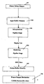
- Figure 1 illustrates the prior art steps required to process the input data that a printer typically receives from a conventional personal computer (PC).
- the output from the PC normally is supplied by a printer driver 101 that prepares an output print file.
- This file includes a set of instructions and data in a page description language (PDL) or compressed bitmap format. These instructions and data may be transported to the printer via IEEE 1284 (Firewire) or Universal Serial Bus (USB) cabling or over a local area network and stored in an input buffer memory 102.
- PDL page description language
- USB Universal Serial Bus
- the first computational step in the printer controller pipeline is interpretation 103 of the data.
- the display list from interpretation 103 includes a description of individual elements of graphics data or text data along with the position of these elements on the page.
- the display list may be in a banded or a non-banded format.
- banded format discrete bands are defined and formed as a part of the processing. After rendering, a number of these bands collectively form a full printer controller output page.
- a non-banded format each page is interpreted as a unit. After rendering, this unit forms an integral part of printer controller output.
- the rendering pipeline stage 104 reduces the interpreted data of the display list to printer specific raster data. This process is sometimes called rasterization.
- the output of the rendering process is a bit map format in which discrete digitized dots (pixels) are generated to control the output device (e.g. ink jet pen, laser drum) with proportions of the colors cyan, yellow, magenta, and black.
- the rendering step is well suited to digital processing operations commonly used in digital signal processor devices.
- the bit map data is stored in an output buffer memory stage 105. This bit map data is sent as needed to the printer output mechanism 106.
- FIG. 2 illustrates a high-level view of the full complement of printer pipeline functions of the prior art.
- the input data has a variety of sources, such as spooled jobs on disc 201, parallel printer port 202, Universal Serial Bus (USB) port 203, Ethernet TCP/IP port 204 and IEEE 1284 (Firewire) 205.
- Each data source has its specific data format. This data must be reduced to a common format for processing in the pipeline.
- Streams interface unit 207 adjusts the format of the input data as required. For example, data arrives in parallel form from parallel printer port 202 and is converted in streams interface unit 207 as necessary for uniform processing in later stages. Likewise, streams interface unit 207 often carries out format adjustments upon data from USB port 203 in queue coming from the host processor.
- Streams interface unit 207 sends data to the path that performs parallel interpretation of the composite postscript 208, printer control language PCL 210 or other PDL interpreter 210.
- Page pipeline block 209 re-assembles the results of the interpretation process into page format for page oriented processing before submitting page data to rendering unit 212.
- Postscript interpreter 208 or PCL interpreter 210 may send banded format data directly to rendering unit 212.
- Rendering unit 212 also performs compression, decompression or screening as required.
- PDL print controller to print engine controller interface unit 225 supplies data and control information to ASIC special purpose processor 213 to drive paper path control 216, the control panel/display 214 and the video data output 215.
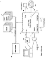
- Figure 3 illustrates a conventional printer controller system.
- the system has typically a main processor 300 and a system ASIC printer controller 301, both served by a single processor bus 302. All major compute functions are carried out within the main processor 300.
- the system interfacing to a personal computer (PC) 303 is directed by the system ASIC printer controller 301 via a USB port 304 or alternately by an IEEE 1284 (Firewire) compatible parallel port 305.
- ASIC printer controller 301 directs networking by the system via the Ethernet 306 from a local area network 307 and provides a mass storage interface via an ATA-4 compatible disc interface 308 to disc drive 309.
- System data movement among main processor 300, system ASIC print controller 301, synchronous dynamic random access memory (SDRAM) 310 and read only memory (ROM) or FLASH memory 311 are all accomplished via processor bus 302.
- System ASIC print controller 301 provides interface to printer engine via engine control signals 312 and video data output 313.
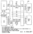
- FIG. 4 illustrates the organization of a digital signal processor system 300 to which this invention is applicable. This description corresponds to a TMS320C6211 digital signal processor sold by Texas Instruments. Other digital signal processors or general purpose processors may be used to embody this invention. In order to be useful in this invention the processor must have a high bandwidth access to memory. This will be further explained below.
- Digital signal processor system 300 includes central processing unit core 410.
- Central processing unit core 410 includes the data processing portion of digital signal processor system 300.
- Central processing unit core 410 could be constructed as known in the art and would typically includes a register file, an integer arithmetic logic unit, an integer multiplier and program flow control units.
- Digital signal processor system 300 includes a number of cache memories.
- Figure 4 illustrates a pair of first level caches.
- Level one instruction cache (L1I) 421 stores instructions used by central processing unit core 410.
- Central processing unit core 410 first attempts to access any instruction from level one instruction cache 421.
- Level one data cache (L1D) 423 stores data used by central processing unit core 410.
- Central processing unit core 410 first attempts to access any required data from level one data cache 423.
- the two level one caches are backed by a level two unified cache (L2) 430. In the event of a cache miss to level one instruction cache 421 or to level one data cache 423, the requested instruction or data is sought from level two unified cache 430.
- L2 level two unified cache
- the requested instruction or data is stored in level two unified cache 430, then it is supplied to the requesting level one cache for supply to central processing unit core 410.
- the requested instruction or data may be simultaneously supplied to both the requesting cache and central processing unit core 410 to speed use.
- Level two unified cache 430 is further coupled to higher level memory systems.
- Digital signal processor system 300 may be a part of a multiprocessor system.
- the other processors of the multiprocessor system are coupled to level two unified cache 430 via a transfer request bus 441 and a data transfer bus 443.
- a direct memory access unit 450 provides the connection of digital signal processor system 300 to external memory including SDRAM 310 and ROM/FLASH memory 311 and the system ASIC print controller 301.
- the exemplary TMS320C6211 allows a single memory to be selectively partitioned into unified level two cache 430 and directly accessible static random access memory 435.
- the proportions of the cache and SRAM provided may vary form all cache to all SRAM. This is illustrated by the dashed line dividing unified level two cache 430 and directly addressable SRAM 435.
- SRAM 435 When configured to include a non-zero amount of SRAM, SRAM 435 is accessible as normal read/write memory which operates under program control.
- This memory space may be either a source or a destination of a direct memory access.
- digital signal processor 300 must be configured with at least some SRAM. Note that a memory selectively partitionable between cache and SRAM is not required for this invention. This invention merely requires the existence of some on-chip SRAM, which may be separate form any cache.
- level one instruction cache 421 may receive instructions recalled from level two unified cache 430 (1) for a cache miss fill.
- level two unified cache 430 there is no hardware support for self-modifying code so that instructions stored in level one instruction cache 421 are not altered.
- the first of these data movements is a cache miss fill from level two unified cache 430 to level one data cache 423 (2).
- Data may also pass from level one data cache 423 to level two unified cache 430 (3).
- This data movement takes place upon; a write miss to level one data cache 423 which must be serviced by level two unified cache 430; a victim eviction from level one data cache 423 to level two unified cache 430; and a snoop response from level one data cache 423 to level two unified cache 430.
- Data can be moved between level two unified cache 430 of SRAM 435 and external memory 310/311. This can take place upon: a cache miss to level two unified cache 430 service from external memory (4) or a direct memory access 450 data movement from external memory 310/311 to SRAM 435; a victim eviction from level two unified cache 430 to external memory 461 (5) or a direct memory access 450 data movement from SRAM 435 to external memory 310.
- data can move between level two unified cache 430 and system ASIC 301. These movements take place upon: or a direct memory access 450 data movement from ASIC 310 to SRAM 435; or a direct memory access 450 data movement from SRAM 435 to ASIC 301. All data movement between level two unified cache 430/SRAM 435 and external memory 310/311 and between level two unified cache 430/SRAM 435 and ASIC 301 employ data transfer bus 443 and are controlled by direct memory access unit 450. These direct memory access data movements may take place as result of a command from central processing unit core 410 or a command from another digital signal processor system received via transfer request bus 441.
- FIG. 5 illustrates process 500 of this invention in flow chart form.
- Process 500 is the manner that digital signal processor 300 performs part of rendering pipeline stage 104 illustrated in Figure 1.
- the programmer must allocate memory space within SDRAM 310 to store the rendered page. It is typical to render the page completely into a page buffer before beginning the print engine. This assures that the print engine will not stall for lack of data and spoil a page.
- the print engine operates at a single speed and the print data must be available when the photoconductive drum is at the corresponding page location. Depending on the relative print and rendering speeds, it may be possible to race the print engine.
- the print data is compressed following rendering. By storing only the compressed bands, less memory is required.
- the print data is decompressed as needed by the print engine during printing or partially decompressed.
- the page buffer must be divided into sub-bands.
- Digital signal processor 300 will render each sub-band individually.
- the sub-band size must be selected to be less than the size of the on-chip SRAM. It is helpful to align the sub-band boundaries with page buffer memory words. This will be more fully described below.
- Process 500 begins with start block 501.
- Process 500 first sets the current page as the first page and the current sub-band as the first sub-band of the current page description language file to be printed (processing block 502).
- Process 500 parses the display list of the page description language file for the current page to determine which display list elements will render to the current sub-band. Detailed rendering is not required. It is better to falsely determine that a display list element will write to the sub-band than to improperly omit a display list element from this parsed list.
- Process 500 then transfers the parsed list of display elements for the current page and sub-band to SRAM 435 (processing block 504). Additional auxiliary data required to render these display element may also be transferred to the on-chip SRAM.
- This auxiliary data could be fonts, color tables and the like.
- These steps store in data needed for rendering in SRAM 435. This serves to increase the rendering speed because of the high memory bandwidth between central processing unit 410 and SRAM 435. These steps are not necessary to obtain substantial benefit from this invention. Since the display list elements and the auxiliary data probably is less than the rendered sub-band data, the benefit of processing blocks 502 and 503 will not be as great as the benefit from the rendered data.
- Process 500 next sets the current display element to the first display element of the parsed list (processing block 505).
- Process 500 then renders the current display element into the sub-band region of SRAM 435 (processing block 506). This will involve a final determination that the display list element does actually render to the current sub-band. This also involves truncating the rendered data to the current sub-band. This portion of the process is memory bandwidth intensive. Using on-chip SRAM 435 as the target memory insures the maximum available processor/memory bandwidth.
- Process 500 then checks to determine if the current display element is the last display element (decision block 507). If this is not the last display element (No at decision block 507), then process 500 sets the next display element as the current display element (processing block 508). Processing block 500 then returns to processing block 506 to render the new display element into the sub-band memory space of SRAM 435.
- Process 500 transfers the rendered page data from the on-chip SRAM to the page buffer memory. This process is illustrated schematically in Figure 6.
- Rendered page data from SRAM 435 a part of digital signal processor 300, is written into the corresponding sub-band 601 within SDRAM 310.
- the page buffer holds the completely rendered page before transmission to the print engine for printing.
- Process 500 then tests to determine if the current sub-band is the last sub-band (decision block 510). If this is not the case (No at decision block 510), then process 500 sets the next sub-band as the current sub-band (processing block 511) and then returns to processing block 503. This begins the rendering process for the new sub-band.
- Figure 6 illustrates the next sub-band 602 for process 500.
- process 500 prints the current page (processing block 512).
- Process 500 prints the page in the same manner as the prior art by transferring the print data to the print engine and controlling the paper movement and printing process. As discussed above, this print process may include print data compression and decompression to save memory space within SDRAM 310.
- Process 500 then tests to determine if the current page is the last page of the page description language file (decision block 513). If the current page is not the last page of this document (No at decision block 513), the process 500 sets the next page as the current page and the first sub-band as the current sub-band (processing block 514). Process 500 then returns to processing block 503, beginning the process for rendering and printing the new page. If the current page is the last page (Yes at decision block 513), then the document printing is complete. Process 500 ends with end block 516.
- This sub-band process is advantageous due to the nature of rendering. Rendering will often take place at positions other than word boundaries within the memory system.
- the display list of the page description language can specify the print color of any dot on the page.
- These non-aligned writes are typically performed and read-modify-write cycles.
- the whole memory word is read into central processing unit 410.
- the memory word is modified by writing the pixel data in the corresponding location without changing other parts of the memory data word. Then the whole memory data word is written to the main memory. This changes a single write into a combination read and write operation.
- Such non-aligned writes may take place often and depend on the relationship between the length of a memory data word and the length of a pixel data word.
- the rendering may require several read-modify-write cycles to the same memory data word. This could occur if differing display list elements specify pixel data for differing pixels within the same memory word. Differing display list elements often specify differing pixel data for the same pixel. This could occur if one object overlays another. In such a case, a paint analogy is often used with the last specified object controlling the pixel data for that particular pixel.
- SRAM 435 which has a high memory bandwidth connection to central processing unit 410.
- the transfer of rendered data from SRAM 435 to the corresponding sub-band 601 within SDRAM 310 may take place in a burst fashion. This data transfer can be made mostly in whole memory data words. The only possible areas requiring read-modify-write cycles are at the sub-band edges. If the sub-bands are aligned with memory data words, even the edges can be transferred in whole memory data words.
- the memory transfer rate between SRAM 435 and the page buffer within SDRAM 310 is so much slower than the memory transfer rate between central processing unit 410 and SRAM 435, that buffering or caching the rendering in SRAM 435 will generally be advantageous.
Landscapes
- Engineering & Computer Science (AREA)
- General Engineering & Computer Science (AREA)
- Physics & Mathematics (AREA)
- General Physics & Mathematics (AREA)
- Theoretical Computer Science (AREA)
- Record Information Processing For Printing (AREA)
- Image Processing (AREA)
- Storing Facsimile Image Data (AREA)
- Image Generation (AREA)
Applications Claiming Priority (2)
| Application Number | Priority Date | Filing Date | Title |
|---|---|---|---|
| US24765400P | 2000-11-09 | 2000-11-09 | |
| US247654P | 2000-11-09 |
Publications (3)
| Publication Number | Publication Date |
|---|---|
| EP1205876A2 true EP1205876A2 (de) | 2002-05-15 |
| EP1205876A3 EP1205876A3 (de) | 2004-03-31 |
| EP1205876B1 EP1205876B1 (de) | 2008-06-25 |
Family
ID=22935771
Family Applications (1)
| Application Number | Title | Priority Date | Filing Date |
|---|---|---|---|
| EP01000614A Expired - Lifetime EP1205876B1 (de) | 2000-11-09 | 2001-11-09 | Seitenbilderzeugung in einem digitalen Signalprozessor |
Country Status (5)
| Country | Link |
|---|---|
| US (1) | US7050191B2 (de) |
| EP (1) | EP1205876B1 (de) |
| JP (1) | JP2002196904A (de) |
| AT (1) | ATE399347T1 (de) |
| DE (1) | DE60134523D1 (de) |
Families Citing this family (8)
| Publication number | Priority date | Publication date | Assignee | Title |
|---|---|---|---|---|
| US7164489B2 (en) * | 2001-10-19 | 2007-01-16 | Seiko Epson Corporation | Rectangular partitioning in printing rotated images |
| US7809252B2 (en) * | 2003-04-09 | 2010-10-05 | Corel Inc. | Systems and methods for caching multimedia data |
| US7200713B2 (en) * | 2004-03-29 | 2007-04-03 | Intel Corporation | Method of implementing off-chip cache memory in dual-use SRAM memory for network processors |
| CN100360318C (zh) * | 2005-01-31 | 2008-01-09 | 北京北大方正电子有限公司 | 一种能够提高内存利用率的打印内存管理方法 |
| TWI273419B (en) * | 2005-02-05 | 2007-02-11 | Sercomm Corp | Network interfacing system for PictBridge printer |
| US7505170B2 (en) * | 2005-07-13 | 2009-03-17 | Microsoft Corporation | Conversions between spool files and PDL within a pipeline of modular filters |
| JP5424546B2 (ja) * | 2007-09-13 | 2014-02-26 | 京セラドキュメントソリューションズ株式会社 | 画像処理装置及び画像形成システム |
| US8341311B1 (en) * | 2008-11-18 | 2012-12-25 | Entorian Technologies, Inc | System and method for reduced latency data transfers from flash memory to host by utilizing concurrent transfers into RAM buffer memory and FIFO host interface |
Family Cites Families (5)
| Publication number | Priority date | Publication date | Assignee | Title |
|---|---|---|---|---|
| US5218670A (en) * | 1990-08-31 | 1993-06-08 | Texas Instruments Incorporated | Apparatus and methods for the handling of banded frame buffer overflows |
| US5604846A (en) * | 1994-10-13 | 1997-02-18 | Brother Kogyo Kabushiki Kaisha | Printer and method for developing print data |
| WO1996039680A1 (en) | 1995-06-06 | 1996-12-12 | Apple Computer, Inc. | System and method for image generation using compression |
| US6538764B2 (en) * | 1996-04-12 | 2003-03-25 | Canon Kabushiki Kaisha | Printing apparatus, information processing apparatus, data processing method for use in such an apparatus, and storage medium storing computer-readable program |
| EP0825550A3 (de) * | 1996-07-31 | 1999-11-10 | Texas Instruments Incorporated | Druckvorrichtung und -verfahren mit mehreren Prozessoren |
-
2001
- 2001-11-08 JP JP2001343135A patent/JP2002196904A/ja active Pending
- 2001-11-09 DE DE60134523T patent/DE60134523D1/de not_active Expired - Lifetime
- 2001-11-09 EP EP01000614A patent/EP1205876B1/de not_active Expired - Lifetime
- 2001-11-09 US US09/990,841 patent/US7050191B2/en not_active Expired - Lifetime
- 2001-11-09 AT AT01000614T patent/ATE399347T1/de not_active IP Right Cessation
Also Published As
| Publication number | Publication date |
|---|---|
| DE60134523D1 (de) | 2008-08-07 |
| JP2002196904A (ja) | 2002-07-12 |
| US7050191B2 (en) | 2006-05-23 |
| US20020054309A1 (en) | 2002-05-09 |
| ATE399347T1 (de) | 2008-07-15 |
| EP1205876A3 (de) | 2004-03-31 |
| EP1205876B1 (de) | 2008-06-25 |
Similar Documents
| Publication | Publication Date | Title |
|---|---|---|
| EP0887763B1 (de) | Verfahren und Vorrichtung zum Aufbau von Bitmap-Daten in einem Drucker | |
| US6879409B2 (en) | Printing method and apparatus having multiple raster image processors | |
| US9779335B2 (en) | Parallel processing page description language data | |
| US6038033A (en) | Method and apparatus for compressing and decompressing print data in the background operations of a printer | |
| US20030231320A1 (en) | Image processing method and apparatus | |
| JP2009146251A (ja) | 画像処理装置および画像形成システムとプログラム | |
| US8339667B2 (en) | Optimizing to-be printed objects during print job processing | |
| US8498012B2 (en) | Print job management systems and methods | |
| US20020196468A1 (en) | Variable data printing with optimized cache | |
| US7050191B2 (en) | Sub-banding of display list and video buffer for page rendering in a digital signal processor | |
| US20070070403A1 (en) | Information processing apparatus, information processing method, and program | |
| JP3962606B2 (ja) | 印刷命令生成装置及び方法、印刷装置及びその制御方法、情報処理装置及び印刷システム | |
| US6023343A (en) | Method and apparatus for temporary storage on disk of collated print data | |
| US20030011819A1 (en) | Information processing device, information processing method, printing system, computer program and memory medium | |
| US5671246A (en) | Method and apparatus for adaptive adjustment of cache allocation for storage of font data | |
| US5469534A (en) | Method for translating image processing data | |
| KR100571960B1 (ko) | 화상형성장치의 제어장치 및 방법 | |
| EP1116095B1 (de) | Druckverfahren und gerät, das mehrere rasterbildprozessoren hat | |
| KR100246457B1 (ko) | 프린터의화상데이터출력방법 | |
| GB2331824A (en) | Inheriting in page production for a page printer | |
| JP2981758B2 (ja) | ラスタ型プリンタ | |
| JP2005169671A (ja) | データ処理装置および印刷制御方法およびコンピュータが読み取り可能なプログラムを格納した記憶媒体およびプログラム | |
| JPH10124270A (ja) | プリント・システム | |
| US20030174141A1 (en) | Sorting image primitives in generation of image page descriptions | |
| KR19990002293A (ko) | 프린터의 객체 기반 색정합 방법 |
Legal Events
| Date | Code | Title | Description |
|---|---|---|---|
| PUAI | Public reference made under article 153(3) epc to a published international application that has entered the european phase |
Free format text: ORIGINAL CODE: 0009012 |
|
| AK | Designated contracting states |
Kind code of ref document: A2 Designated state(s): AT BE CH CY DE DK ES FI FR GB GR IE IT LI LU MC NL PT SE TR |
|
| AX | Request for extension of the european patent |
Free format text: AL;LT;LV;MK;RO;SI |
|
| PUAL | Search report despatched |
Free format text: ORIGINAL CODE: 0009013 |
|
| AK | Designated contracting states |
Kind code of ref document: A3 Designated state(s): AT BE CH CY DE DK ES FI FR GB GR IE IT LI LU MC NL PT SE TR |
|
| AX | Request for extension of the european patent |
Extension state: AL LT LV MK RO SI |
|
| RIC1 | Information provided on ipc code assigned before grant |
Ipc: 7G 06K 15/00 A |
|
| 17P | Request for examination filed |
Effective date: 20040930 |
|
| AKX | Designation fees paid |
Designated state(s): AT BE CH CY DE DK ES FI FR GB GR IE IT LI LU MC NL PT SE TR |
|
| GRAP | Despatch of communication of intention to grant a patent |
Free format text: ORIGINAL CODE: EPIDOSNIGR1 |
|
| GRAS | Grant fee paid |
Free format text: ORIGINAL CODE: EPIDOSNIGR3 |
|
| GRAA | (expected) grant |
Free format text: ORIGINAL CODE: 0009210 |
|
| AK | Designated contracting states |
Kind code of ref document: B1 Designated state(s): AT BE CH CY DE DK ES FI FR GB GR IE IT LI LU MC NL PT SE TR |
|
| REG | Reference to a national code |
Ref country code: GB Ref legal event code: FG4D |
|
| REG | Reference to a national code |
Ref country code: CH Ref legal event code: EP |
|
| REF | Corresponds to: |
Ref document number: 60134523 Country of ref document: DE Date of ref document: 20080807 Kind code of ref document: P |
|
| REG | Reference to a national code |
Ref country code: IE Ref legal event code: FG4D |
|
| PG25 | Lapsed in a contracting state [announced via postgrant information from national office to epo] |
Ref country code: FI Free format text: LAPSE BECAUSE OF FAILURE TO SUBMIT A TRANSLATION OF THE DESCRIPTION OR TO PAY THE FEE WITHIN THE PRESCRIBED TIME-LIMIT Effective date: 20080625 |
|
| PG25 | Lapsed in a contracting state [announced via postgrant information from national office to epo] |
Ref country code: AT Free format text: LAPSE BECAUSE OF FAILURE TO SUBMIT A TRANSLATION OF THE DESCRIPTION OR TO PAY THE FEE WITHIN THE PRESCRIBED TIME-LIMIT Effective date: 20080625 Ref country code: NL Free format text: LAPSE BECAUSE OF FAILURE TO SUBMIT A TRANSLATION OF THE DESCRIPTION OR TO PAY THE FEE WITHIN THE PRESCRIBED TIME-LIMIT Effective date: 20080625 |
|
| NLV1 | Nl: lapsed or annulled due to failure to fulfill the requirements of art. 29p and 29m of the patents act | ||
| PG25 | Lapsed in a contracting state [announced via postgrant information from national office to epo] |
Ref country code: PT Free format text: LAPSE BECAUSE OF FAILURE TO SUBMIT A TRANSLATION OF THE DESCRIPTION OR TO PAY THE FEE WITHIN THE PRESCRIBED TIME-LIMIT Effective date: 20081125 Ref country code: ES Free format text: LAPSE BECAUSE OF FAILURE TO SUBMIT A TRANSLATION OF THE DESCRIPTION OR TO PAY THE FEE WITHIN THE PRESCRIBED TIME-LIMIT Effective date: 20081006 Ref country code: SE Free format text: LAPSE BECAUSE OF FAILURE TO SUBMIT A TRANSLATION OF THE DESCRIPTION OR TO PAY THE FEE WITHIN THE PRESCRIBED TIME-LIMIT Effective date: 20080925 |
|
| PG25 | Lapsed in a contracting state [announced via postgrant information from national office to epo] |
Ref country code: BE Free format text: LAPSE BECAUSE OF FAILURE TO SUBMIT A TRANSLATION OF THE DESCRIPTION OR TO PAY THE FEE WITHIN THE PRESCRIBED TIME-LIMIT Effective date: 20080625 |
|
| PG25 | Lapsed in a contracting state [announced via postgrant information from national office to epo] |
Ref country code: DK Free format text: LAPSE BECAUSE OF FAILURE TO SUBMIT A TRANSLATION OF THE DESCRIPTION OR TO PAY THE FEE WITHIN THE PRESCRIBED TIME-LIMIT Effective date: 20080625 |
|
| PLBE | No opposition filed within time limit |
Free format text: ORIGINAL CODE: 0009261 |
|
| STAA | Information on the status of an ep patent application or granted ep patent |
Free format text: STATUS: NO OPPOSITION FILED WITHIN TIME LIMIT |
|
| 26N | No opposition filed |
Effective date: 20090326 |
|
| PG25 | Lapsed in a contracting state [announced via postgrant information from national office to epo] |
Ref country code: MC Free format text: LAPSE BECAUSE OF NON-PAYMENT OF DUE FEES Effective date: 20081130 |
|
| REG | Reference to a national code |
Ref country code: CH Ref legal event code: PL |
|
| PG25 | Lapsed in a contracting state [announced via postgrant information from national office to epo] |
Ref country code: IT Free format text: LAPSE BECAUSE OF FAILURE TO SUBMIT A TRANSLATION OF THE DESCRIPTION OR TO PAY THE FEE WITHIN THE PRESCRIBED TIME-LIMIT Effective date: 20080625 |
|
| PG25 | Lapsed in a contracting state [announced via postgrant information from national office to epo] |
Ref country code: IE Free format text: LAPSE BECAUSE OF NON-PAYMENT OF DUE FEES Effective date: 20081109 Ref country code: CH Free format text: LAPSE BECAUSE OF NON-PAYMENT OF DUE FEES Effective date: 20081130 Ref country code: LI Free format text: LAPSE BECAUSE OF NON-PAYMENT OF DUE FEES Effective date: 20081130 |
|
| PG25 | Lapsed in a contracting state [announced via postgrant information from national office to epo] |
Ref country code: CY Free format text: LAPSE BECAUSE OF FAILURE TO SUBMIT A TRANSLATION OF THE DESCRIPTION OR TO PAY THE FEE WITHIN THE PRESCRIBED TIME-LIMIT Effective date: 20080625 Ref country code: LU Free format text: LAPSE BECAUSE OF NON-PAYMENT OF DUE FEES Effective date: 20081109 |
|
| PG25 | Lapsed in a contracting state [announced via postgrant information from national office to epo] |
Ref country code: TR Free format text: LAPSE BECAUSE OF FAILURE TO SUBMIT A TRANSLATION OF THE DESCRIPTION OR TO PAY THE FEE WITHIN THE PRESCRIBED TIME-LIMIT Effective date: 20080625 |
|
| PG25 | Lapsed in a contracting state [announced via postgrant information from national office to epo] |
Ref country code: GR Free format text: LAPSE BECAUSE OF FAILURE TO SUBMIT A TRANSLATION OF THE DESCRIPTION OR TO PAY THE FEE WITHIN THE PRESCRIBED TIME-LIMIT Effective date: 20080926 |
|
| REG | Reference to a national code |
Ref country code: FR Ref legal event code: PLFP Year of fee payment: 15 |
|
| REG | Reference to a national code |
Ref country code: FR Ref legal event code: PLFP Year of fee payment: 16 |
|
| REG | Reference to a national code |
Ref country code: FR Ref legal event code: PLFP Year of fee payment: 17 |
|
| REG | Reference to a national code |
Ref country code: FR Ref legal event code: PLFP Year of fee payment: 18 |
|
| PGFP | Annual fee paid to national office [announced via postgrant information from national office to epo] |
Ref country code: DE Payment date: 20191017 Year of fee payment: 19 |
|
| PGFP | Annual fee paid to national office [announced via postgrant information from national office to epo] |
Ref country code: FR Payment date: 20191029 Year of fee payment: 19 |
|
| PGFP | Annual fee paid to national office [announced via postgrant information from national office to epo] |
Ref country code: GB Payment date: 20191029 Year of fee payment: 19 |
|
| REG | Reference to a national code |
Ref country code: DE Ref legal event code: R119 Ref document number: 60134523 Country of ref document: DE |
|
| GBPC | Gb: european patent ceased through non-payment of renewal fee |
Effective date: 20201109 |
|
| PG25 | Lapsed in a contracting state [announced via postgrant information from national office to epo] |
Ref country code: FR Free format text: LAPSE BECAUSE OF NON-PAYMENT OF DUE FEES Effective date: 20201130 |
|
| PG25 | Lapsed in a contracting state [announced via postgrant information from national office to epo] |
Ref country code: GB Free format text: LAPSE BECAUSE OF NON-PAYMENT OF DUE FEES Effective date: 20201109 Ref country code: DE Free format text: LAPSE BECAUSE OF NON-PAYMENT OF DUE FEES Effective date: 20210601 |