EP1205977A2 - Memory device with central connecting area - Google Patents
Memory device with central connecting area Download PDFInfo
- Publication number
- EP1205977A2 EP1205977A2 EP01126398A EP01126398A EP1205977A2 EP 1205977 A2 EP1205977 A2 EP 1205977A2 EP 01126398 A EP01126398 A EP 01126398A EP 01126398 A EP01126398 A EP 01126398A EP 1205977 A2 EP1205977 A2 EP 1205977A2
- Authority
- EP
- European Patent Office
- Prior art keywords
- field
- row
- cell
- connection
- connection field
- Prior art date
- Legal status (The legal status is an assumption and is not a legal conclusion. Google has not performed a legal analysis and makes no representation as to the accuracy of the status listed.)
- Ceased
Links
Images

Classifications
-
- G—PHYSICS
- G11—INFORMATION STORAGE
- G11C—STATIC STORES
- G11C5/00—Details of stores covered by group G11C11/00
- G11C5/02—Disposition of storage elements, e.g. in the form of a matrix array
-
- G—PHYSICS
- G11—INFORMATION STORAGE
- G11C—STATIC STORES
- G11C5/00—Details of stores covered by group G11C11/00
- G11C5/02—Disposition of storage elements, e.g. in the form of a matrix array
- G11C5/025—Geometric lay-out considerations of storage- and peripheral-blocks in a semiconductor storage device
-
- H—ELECTRICITY
- H10—SEMICONDUCTOR DEVICES; ELECTRIC SOLID-STATE DEVICES NOT OTHERWISE PROVIDED FOR
- H10B—ELECTRONIC MEMORY DEVICES
- H10B12/00—Dynamic random access memory [DRAM] devices
- H10B12/30—DRAM devices comprising one-transistor - one-capacitor [1T-1C] memory cells
-
- H—ELECTRICITY
- H10—SEMICONDUCTOR DEVICES; ELECTRIC SOLID-STATE DEVICES NOT OTHERWISE PROVIDED FOR
- H10W—GENERIC PACKAGES, INTERCONNECTIONS, CONNECTORS OR OTHER CONSTRUCTIONAL DETAILS OF DEVICES COVERED BY CLASS H10
- H10W72/00—Interconnections or connectors in packages
-
- H—ELECTRICITY
- H10—SEMICONDUCTOR DEVICES; ELECTRIC SOLID-STATE DEVICES NOT OTHERWISE PROVIDED FOR
- H10W—GENERIC PACKAGES, INTERCONNECTIONS, CONNECTORS OR OTHER CONSTRUCTIONAL DETAILS OF DEVICES COVERED BY CLASS H10
- H10W72/00—Interconnections or connectors in packages
- H10W72/90—Bond pads, in general
Definitions
- a third and fourth row 17, 18 is formed, which are mirror-symmetrical to the first and second rows 15, 16 are arranged in the connection field 1.
- a fifth and sixth row 20, 19 of bond pads 14 is in each case in one predetermined distance and arranged parallel to the longitudinal edges.
- the fifth and sixth rows 19, 20 are in the Intermediate region arranged which the first and second or third and fourth rows 15, 16, 17, 18 are spaced apart. In this way, a symmetrical distribution of the Bondpads 14 reached. So there is a lot of space for one Welding the bond pads 14 given with bond wires and in addition, the cell fields are almost the same size Distance arranged around the bond pads. However, there are others Arrangements of bond pads such as the arrangement in one Row possible.
- FIG. 2 shows a further embodiment of a memory arrangement, compared to the memory arrangement of the Fig. 1, the previous cell fields 2 to 9 in each case first and second sub-cell field 21, 22 are divided.
- Each sub-cell array 21, 22 has its own row decoder 11 on.
- Each cell field 2 to 9 thus has one Row decoder 10 and two row decoders 11. So that is data access to the data of a row selection line faster because the bit lines are shorter.
Landscapes
- Engineering & Computer Science (AREA)
- Microelectronics & Electronic Packaging (AREA)
- Dram (AREA)
- Semiconductor Memories (AREA)
Abstract
Es wird eine Speicheranordnung beschrieben, die ein zentrales Anschlussfeld (1) aufweist. Das zentrale Anschlussfeld ist kranzförmig von Zellenfeldern (2-9) mit Speicherzellen umgeben. Auf diese Weise wird eine Speicheranordnung mit kompakten Außenmaßen bereitgestellt, die sich insbesondere für ein Seitenverhältnis von 2:1 eignet. Im zentralen Anschlussfeld sind vorzugsweise alle Peripherieschaltungen (23) angeordnet. Dadurch sind die Laufzeitunterschiede zwischen den Peripherieschaltungen und den verschiedenen Zellenfeldern relativ gering.A memory arrangement is described which has a central connection field (1). The central connection field is surrounded by cell fields (2-9) with memory cells. In this way, a memory arrangement with compact external dimensions is provided, which is particularly suitable for an aspect ratio of 2: 1. All peripheral circuits (23) are preferably arranged in the central connection panel. As a result, the runtime differences between the peripheral circuits and the various cell fields are relatively small.
Description
Die Erfindung betrifft eine Speicheranordnung gemäß dem
Oberbegriff des Patentanspruchs 1.The invention relates to a memory arrangement according to the
Preamble of
Halbleiterspeicher werden typischerweise aus kleinen, regulären
Zelleneinheiten aufgebaut (z.B. bestehen beim 256 Mb-DRAM
die Zelleneinheiten aus 4 Mb). Diese Zelleneinheiten
werden zu größeren Anordnungen zusammengefasst (Zellenfelder),
die beim 256 Mb-DRAM wiederum häufig 64 Mb groß sind.
Beim 256 M-DRAM müssen somit vier dieser Zellenfelder auf
dem Baustein angeordnet werden, wobei häufig jeweils zwei
Zellenfelder nebeneinander angeordnet sind und zwischen
zwei nebeneinander angeordneten Zellenfeldern ein Anschlussfeld
ausgebildet ist. Das Anschlussfeld weist
Bondpads auf, die mit dem Schaltelementen der Zellenfelder
verbunden sind und zum Anschluss von weiteren Schaltungen
dienen. Da ein einzelnes Zellenfeld häufig ein Seitenverhältnis
von 2:1 hat, und das Anschlussfeld relativ klein
ist, ergibt sich z. B. bei dem 256 Mb-DRAM mit vier Zellenfeldern
direkt ein Gesamt-Seitenverhältnis von 2:1. Bei einem
512 M-DRAM, bei welchem dann acht Zellenfelder (512M =
8*64M) platziert werden müssen, bleiben nun im Stand der
Technik zwei Alternativen:
Die Aufgabe der Erfindung besteht darin, Speicherfelder mit einem flexibleren Aufbau bereitzustellen.The object of the invention is to use memory fields to provide a more flexible structure.
Die Aufgabe der Erfindung wird durch die Merkmale des Anspruchs
1 gelöst. Ein wesentlicher Vorteil der Erfindung
besteht darin, dass ein mittig angeordnetes Anschlussfeld
vorgesehen ist, das ringförmig von Zellenfeldern umgeben
ist. Auf diese Weise wird eine sehr kompakte Anordnung einer
Vielzahl von Zellenfeldern in einer Speicheranordnung
erreicht.The object of the invention is achieved by the features of the
Weitere vorteilhafte Ausführungsformen der Erfindung sind in den abhängigen Ansprüchen angegeben.Further advantageous embodiments of the invention are specified in the dependent claims.
Weiterhin ist es vorteilhaft, das Anschlussfeld und die Zellenfelder rechteckförmig auszubilden, wobei an jeder Seitenkante des Anschlussfeldes ein Zellenfeld mit entsprechend großer Seitenkante angrenzt. In den Eckbereichen des Anschlussfeldes ist jeweils ein weiteres Zellenfeld angeordnet. Diese Ausführungsform der Speicheranordnung weist eine rechteckförmige Außenkontur auf. Damit ist die Speicheranordnung für ein Standardgehäuse mit einem Seitenkantenverhältnis von 2:1 besonders geeignet.It is also advantageous to use the connector panel and the To form cell fields rectangular, with each Side edge of the connection field with a cell field accordingly large side edge adjoins. In the corner areas a further cell field is arranged in each case of the connection field. This embodiment of the memory arrangement exhibits a rectangular outer contour. So that's it Storage arrangement for a standard housing with a side edge ratio of 2: 1 particularly suitable.
Eine vorteilhafte Ausführungsform der Erfindung besteht darin, dass in den Bereichen der Seitenkanten eines Zellenfeldes, das an ein anderes Zellenfeld oder an das Anschlussfeld angrenzt, ein Zeilendecoder oder ein Reihendecoder ausgebildet ist. Auf diese Weise sind der Zeilen- oder Reihendecoder relativ nahe am zentralen Anschlussfeld angeordnet, so dass die Signalwege zum Auslesen oder Einschreiben von Daten in die Zellenfelder relativ kurz sind. An advantageous embodiment of the invention exists in that in the areas of the side edges of a cell field, that to another cell field or to that Connection field adjacent, a row decoder or a row decoder is trained. In this way, the row or row decoder relatively close to the central connection panel arranged so that the signal paths for reading or writing of data in the cell fields are relatively short.
Vorzugsweise weist ein Zellenfeld die annähernd gleiche Größe wie das Anschlussfeld auf.A cell field preferably has approximately the same Size like the connector panel.
In einer weiteren Ausführungsform der Erfindung ist jedes Zellenfeld noch einmal in zwei Unterzellenfelder unterteilt.In another embodiment of the invention, each Cell field divided again into two sub-cell fields.
In einer bevorzugten Ausführungsform sind die Bondpads im Anschlussfeld in Form von vier Reihen angeordnet, wobei die vier Reihen parallel zu den vier Außenkanten des Anschlussfeldes angeordnet sind. Auf diese Weise wird eine symmetrische Verteilung der Anschlusspads ermöglicht.In a preferred embodiment, the bond pads are in the Connection field arranged in the form of four rows, the four rows parallel to the four outer edges of the connection panel are arranged. This way it becomes symmetrical Distribution of the connection pads enables.
Weiterhin ist es vorteilhaft, Peripherieschaltungen im zentralen Anschlussfeld anzuordnen. Damit sind die Peripherieschaltungen von allen Zellenfeldern nahezu gleich weit entfernt, so dass Laufzeitunterschiede zwischen den Signalen verschiedener Zellenfelder relativ gering sind.It is also advantageous to have peripheral circuits in the central To arrange the connection panel. So that are the peripheral circuits almost the same distance from all cell fields, so that runtime differences between the signals different cell fields are relatively small.
Die Erfindung wird im folgenden anhand der Figuren näher erläutert. Es zeigen:
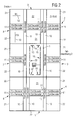
- Fig. 1
- eine erste Speicheranordnung,
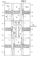
- Fig. 2
- eine zweite Ausführungsform einer Speicheranordnung, und
- Fig. 3
- eine dritte Ausführungsform einer Speicheranordnung.
- Fig. 1
- a first storage arrangement,
- Fig. 2
- a second embodiment of a memory arrangement, and
- Fig. 3
- a third embodiment of a memory arrangement.
Fig. 1 zeigt eine Speicheranordnung, die in der Außenkontur
rechteckförmig aufgebaut ist. Eine Längskante 24 der
Speicheranordnung ist nahezu doppelt so lang, wie eine
Querkante 25 der Speicheranordnung. Somit ist die
Speicheranordnung zum Einbau in eine Standardgehäuse mit
einem Seitenverhältnis von ungefähr 2:1 geeignet. Dieses
Seitenverhältnis wird beispielsweise bei einer Speicherzwischengröße
von 128 Megabit, 512 Megabit, 2 Gigabit usw.
eingesetzt. Aufgrund der Außenkonturen der Speicheranordnungen
ist es möglich, z.B. den 512 Megabit DRAM bereits
eine Technologiegeneration früher in ein Standardgehäuse
einzubauen als in Architekturen des Standes der Technik.Fig. 1 shows a storage arrangement in the outer contour
is rectangular. A
In der Mitte der Speicheranordnung ist ein Anschlussfeld 1
angeordnet, das rechteckförmig ausgebildet ist. Das Seitenverhältnis
des Anschlussfeldes 1 weist ein Verhältnis der
Längsseite zur Querseite von ungefähr 2:1 auf. Im Anschlussfeld
1 sind Bondpads 14 ausgebildet, die in Form von
Reihen angeordnet sind. Ein Bondpad 14 dient zum Anschluss
eines Bonddrahtes, der vom Bondpad zu Anschlusspins eines
Gehäuses geführt ist. Die Bondpads sind an Schaltungen und
Zellenfelder angeschlossen. Die Reihen 15, 16, 17, 18, 19,
20 sind jeweils parallel und in einem vorgegebenen Abstand
zu der Querkante und der Längskante des Anschlussfeldes 1
angeordnet. In dem beschriebenen Ausführungsbeispiel ist
eine erste und zweite Reihe 15, 16 in einem vorgegebenen
Abstand zur oberen Querkante des Anschlussfeldes 1 angeordnet,
wobei die erste und die zweite Reihe 15, 16 wiederum
einen vorgegebenen Abstand zueinander aufweisen und symmetrisch
jeweils einen gleichgroßen Abstand zu den zwei
Längskanten aufweisen.In the middle of the storage arrangement there is a
Weiterhin ist eine dritte und vierte Reihe 17, 18 ausgebildet,
die spiegelsymmetrisch zur ersten und zweiten Reihe
15, 16 im Anschlussfeld 1 angeordnet sind. Eine fünfte und
sechste Reihe 20, 19 von Bondpads 14 ist jeweils in einem
vorgegebenen Abstand und parallel zu den Längskanten angeordnet.
Die fünfte und sechste Reihe 19, 20 sind in dem
Zwischenbereich angeordnet, die die erste und zweite bzw.
dritte und vierte Reihe 15, 16, 17, 18 beabstandet sind.
Auf diese Weise wird eine symmetrische Verteilung der
Bondpads 14 erreicht. Damit ist relativ viel Platz für ein
Verschweißen der Bondpads 14 mit Bonddrähten gegeben und
zudem sind die Zellenfelder nahezu mit einem gleichgroßen
Abstand um die Bondpads angeordnet. Es sind jedoch auch andere
Anordnungen von Bondpads wie z.B. die Anordnung in einer
Reihe möglich.Furthermore, a third and
Das Anschlussfeld 1 ist in Form eines Kranzes mit einem
ersten, zweiten, dritten, vierten, fünften, sechsten, siebten,
achten Zellenfeld 2, 3, 4, 5, 6, 7, 8, 9 umgeben, wobei
die Zellenfelder in der Form und in der Größe entsprechend
dem Anschlussfeld 1 ausgebildet sind. Ein Zellenfeld
stellt ein matrixförmiges Speicherfeld mit Speicherzellen
dar. Zudem ist an jeder Längs- und Querkante des Anschlussfeldes
1 ein Zellenfeld angeordnet, so dass jeweils
zwei Zellenfelder 9, 5 mit jeweils einer Querkante an der
oberen bzw. unteren Querkante des Anschlussfeldes 1 angrenzen
und die Längskanten des vierten und achten Zellenfeldes
5, 9 und des Anschlussfeldes 1 eine gerade Linie bilden.
Ein zweites und sechstes Zellenfeld 3, 7 grenzt jeweils mit
einer Seitenkante an eine Seitenkante des Anschlussfeldes
1, wobei das zweite und sechste Zellenfeld 3, 7 in der
Weise angeordnet sind, dass die Querkanten des zweiten, des
sechsten Zellenfeldes und des Anschlussfeldes 1 jeweils
eine gerade Linie bilden.The
In den Eckbereichen sind ein erstes, drittes, fünftes und
siebtes Zellenfeld 2, 4, 6, 8 in der Weise angeordnet, dass
die Außenkanten der Zellenfelder eine rechteckförmige Kontur
bilden. Die Zellenfelder 2 bis 9 sind identisch aufgebaut.
Jedes Zellenfeld weist einen Zeilendecoder 10 mit
Zeilenleitungen 12 und einem Spaltendecoder 11 mit Spaltenleitungen
13 auf. Über den Zeilen- und Reihendecoder 10, 11
werden die einzelnen Speicherzellen des Zellenfeldes kontaktiert,
die sich an jeweiligen Kreuzungspunkten der Zeilenauswahlleitungen
und Reihenauswahlleitungen 12, 13 befinden.
Jeder Zeilendecoder 10 und Reihendecoder 11 ist
elektrisch mit Bondpads 14 verbunden. Die Zeilendecoder 10
sind entlang den Längskanten in den jeweiligen Zellenfeldern
angeordnet. Die Reihendecoder 11 sind angrenzend an
die Querkanten im jeweiligen Zellenfeld angeordnet. Die
Zeilendecoder 10 und Reihendecoder 11 sind immer an Kanten
angeordnet, die an ein Zellenfeld oder ein Anschlussfeld 1
angrenzen. Somit liegen die Zeilendecoder 10 und Reihendecoder
10 relativ nahe am Anschlussfeld 1, so dass die
Signalwege zwischen den Zeilendecodern 10, Reihendecodern
11 und den Anschlusspads 14 bzw. den Peripherieschaltung 23
relativ kurz sind.In the corner areas are a first, third, fifth and
Das Anschlussfeld 1 weist mehrere Peripherieschaltungen 23
auf, die mit Bondpads 14 und/oder mit den Zellenfeldern
elektrisch verbunden sind. Als Peripherieschaltungen sind
beispielsweise Verstärkerschaltungen, Kontroll-Logik und
weitere Schaltungen vorgesehen, die zum Betreiben der
Speicheranordnung notwendig sind.The
Fig. 2 zeigt eine weitere Ausführungsform einer Speicheranordnung,
bei der im Vergleich zu der Speicheranordnung der
Fig. 1 die bisherigen Zellenfelder 2 bis 9 jeweils in ein
erstes und zweites Unterzellenfeld 21, 22 unterteilt sind.
Jedes Unterzellenfeld 21, 22 weist einen eigenen Reihendecoder
11 auf. Somit weist jedes Zellenfeld 2 bis 9 einen
Zeilendecoder 10 und zwei Reihendecoder 11 auf. Damit ist
der Datenzugriff auf die Daten einer Zeilenauswahlleitung
schneller, da die Bitleitungen kürzer sind.2 shows a further embodiment of a memory arrangement,
compared to the memory arrangement of the
Fig. 1, the
Die Zellenfelder 2 bis 9 sind entsprechend der Ausführungsform
der Fig. 1 ringförmig um das Anschlussfeld 1 angeordnet.
Ein weiterer Unterschied zur Ausführungsform der Fig.
1 besteht in der Anordnung der Bondpads 14. Die erste,
zweite, dritte und vierte Reihe 15, 16, 17, 18 der Bondpads
14 ist entsprechend der Fig. 1 angeordnet. Die fünfte und
sechste Reihe 19, 20 ist zwar ebenfalls parallel zu den
Längskanten angeordnet, weist jedoch einen sehr viel kleineren
Abstand zu den Seitenkanten auf und ist zwischen der
ersten, zweiten, dritten und vierten Reihe 14, 15, 16, 17,
18 und den Längskanten angeordnet. Auch sind im Anschlussfeld
1 Peripherieschaltungen 23 ausgebildet.The cell fields 2 to 9 are in accordance with the
Fig. 3 weist eine weitere Ausführungsform einer Speicheranordnung
auf, bei der jedes Zellenfeld 2 bis 9 entsprechend
der Ausführungsform der Fig. 2 in ein erstes und zweites
Unterzellenfeld 21, 22 unterteilt ist. In dieser Ausführungsform
weist jedoch jedes Zellenfeld 2 bis 9 entlang
einer Längskante einen Reihendecoder 11 auf. Zudem sind jeweils
ein Zeilendecoder 10 für ein Unterzellenfeld 21, 22
in jedem Zellenfeld angeordnet. Ansonsten entspricht der
Aufbau der Zellenfelder dem Aufbau der Fig. 2.3 shows a further embodiment of a memory arrangement
on, in which each
Ein weiterer Unterschied zur Fig. 2 besteht in der Anordnung
der Bondpads 14 im Anschlussfeld 1. Zwar sind die
erste, zweite, dritte und vierte Reihe 14, 15, 16, 17, 18
entsprechend der Fig. 2 angeordnet. Die fünfte und sechste
Reihe 19, 20 sind parallel zu den Längskanten ausgebildet.
Die fünfte Reihe 19 ist zwischen der zweiten und vierten
Reihe 16, 18, die sechste Reihe 20 ist zwischen der ersten
und der dritten Reihe 15, 17 angeordnet. Ebenfalls sind im
Anschlussfeld 1 Peripherieschaltungen 23 integriert.Another difference from FIG. 2 is the arrangement
of the
Vorzugsweise sind alle Peripherieschaltungen, die zum Betreiben der Speicheranordnung notwendig sind, im ersten Anschlussfeld der Speicheranordnungen der Figuren 1, 2, 3 angeordnet.Preferably all peripheral circuits are used to operate the memory arrangement are necessary in the first connection panel the memory arrangements of Figures 1, 2, 3 arranged.
Claims (9)
wobei das Anschlussfeld (1) Anschlusspads aufweist, die mit den Zellenfeldern (2 bis 9) elektrisch verbunden sind, dadurch gekennzeichnet, dass das Anschlussfeld (1) mittig angeordnet ist,
dass an jeder der vier Seitenkanten des Anschlussfeldes (1) jeweils ein Zellenfeld (2 bis 9) anliegt,
dass die Zellenfelder (2 bis 9) in einem geschlossenen Kranz um das Anschlussfeld herum angeordnet sind,
dass ein Zellenfeld (2) mit jeweils zwei Seitenkanten an zwei andere Zellenfelder (3,9) angrenzt,
dass ein Zellenfeld (2 bis 9) in der Längsrichtung in ein erstes und ein zweites Unterzellenfeld (21, 22) unterteilt ist, dass das erste und das zweite Unterzellenfeld (21, 22) entlang der Längsseite, die an das Anschlussfeld (1) oder ein anderes Zellenfeld (2 bis 9) angrenzt, einen Zeilen- oder Reihendecoder (10, 11) aufweist,
dass das Zellenfeld (2 bis 9) in der Mitte der Längsseite zwei aneinander angrenzende Reihen- oder Zeilendecoder (10, 11) aufweist,
dass ein erster Reihen- oder Zeilendecoder (10, 11) mit ersten Adressleitungen (12, 13) verbunden ist, die parallel zur Längsrichtung im ersten Unterzellenfeld (21) angeordnet sind,
dass ein zweiter Reihen- oder Zeilendecoder (10, 11) mit zweiten Adressleitungen (12,13) verbunden ist, die parallel zur Längsrichtung im zweiten Unterzellenfeld (22) angeordnet sind.Memory arrangement with a connection field (1) and with cell fields (2 to 9) which adjoin the connection field (1), a cell field (2 to 9) having a matrix-like memory with row and column decoders (10, 11), each are connected to address lines (12, 13),
wherein the connection field (1) has connection pads which are electrically connected to the cell fields (2 to 9), characterized in that the connection field (1) is arranged in the center,
that a cell field (2 to 9) is applied to each of the four side edges of the connection field (1),
that the cell fields (2 to 9) are arranged in a closed ring around the connection field,
that a cell field (2) with two side edges each adjoins two other cell fields (3,9),
that a cell field (2 to 9) is divided in the longitudinal direction into a first and a second sub-cell field (21, 22), that the first and the second sub-cell field (21, 22) along the long side, which are connected to the connection field (1) or another cell field (2 to 9) is adjacent, has a row or row decoder (10, 11),
that the cell array (2 to 9) has two adjacent row or row decoders (10, 11) in the middle of the long side,
that a first row or row decoder (10, 11) is connected to first address lines (12, 13) which are arranged parallel to the longitudinal direction in the first sub-cell array (21),
that a second row or row decoder (10, 11) is connected to second address lines (12, 13) which are arranged parallel to the longitudinal direction in the second sub-cell array (22).
das Anschlussfeld (1) rechteckförmig ausgebildet ist,
dass die Zellenfelder (2 bis 9) rechteckförmig ausgebildet sind,
dass an die Seitenkanten des Anschlussfeldes (1) vier Zellenfelder (3, 5, 7, 9) mit je einer Seitenkante angrenzen, deren Länge gleich der Länge der Seitenkanten des Anschlussfeldes (1) ist,
dass in den vier Eckbereichen jeweils ein Zellenfeld (2, 4, 6, 8) angeordnet ist,
dass die Gesamtfläche der Speicheranordnung rechteckförmig ausgebildet ist.Memory arrangement according to claim 1, characterized in that
the connection field (1) is rectangular,
that the cell fields (2 to 9) are rectangular in shape,
that four cell fields (3, 5, 7, 9), each with a side edge whose length is equal to the length of the side edges of the connection field (1), adjoin the side edges of the connection field (1),
that a cell field (2, 4, 6, 8) is arranged in each of the four corner areas,
that the total area of the storage arrangement is rectangular.
dass die erste und zweite bzw. die dritte und vierte Reihe auf einer Linie angeordnet sind und einen vorgegebenen Abstand voneinander aufweisen,
dass die fünfte und die sechste Reihe (19, 20) jeweils mittig zu der ersten und dritten bzw. der zweiten und vierten Reihe (15, 17, 16, 18) angeordnet sind. Memory arrangement according to claim 1 or 2, characterized in that a fifth and a sixth row of connection pads (14) are arranged at a predetermined distance parallel to the long sides of the connection field (1), that a first, second, third and fourth row (15 , 16, 17, 18) of connection pads are arranged at a predetermined distance parallel to the transverse sides of the connection field (1),
that the first and second or the third and fourth rows are arranged on a line and have a predetermined distance from one another,
that the fifth and the sixth row (19, 20) are each arranged in the center of the first and third or the second and fourth row (15, 17, 16, 18).
dass eine erste, zweite, dritte und vierte Reihe von Anschlusspads in einem vorgegebenen Abstand parallel zu den Querseiten des Anschlussfeldes (1) angeordnet sind,
dass die erste und zweite bzw. die dritte und die vierte Reihe (15, 16, 17, 18) auf einer Linie angeordnet sind und einen vorgegebenen Abstand voneinander aufweisen,
dass die fünfte und die sechste Reihe (19, 20) jeweils zwischen der ersten und zweiten bzw. der dritten und vierten Reihe (15, 16, 17, 18) angeordnet sind.Memory arrangement according to claim 1 or 2, characterized in that a fifth and a sixth row of connection pads are arranged at a predetermined distance parallel to the long sides of the connection field,
that a first, second, third and fourth row of connection pads are arranged at a predetermined distance parallel to the transverse sides of the connection field (1),
that the first and second or the third and fourth rows (15, 16, 17, 18) are arranged on a line and have a predetermined distance from one another,
that the fifth and the sixth row (19, 20) are each arranged between the first and second or the third and fourth row (15, 16, 17, 18).
dass eine erste, zweite, dritte und vierte Reihe (15, 16, 17, 18) von Anschlusspads (14) in einem vorgegebenen Abstand parallel zu den Querseiten des Anschlussfeldes (1) angeordnet sind,
dass die erste und zweite bzw. die dritte und vierte Reihe (15, 16, 17, 18) auf einer Linie angeordnet sind und einen vorgegebenen Abstand voneinander aufweisen,
dass die fünfte und die sechste Reihe (19, 20 jeweils zwischen der ersten und dritten bzw. der zweiten und vierten Reihe (15, 17, 16, 18) und den Längskanten des Anschlussfeldes (1) angeordnet sind.Memory arrangement according to Claim 1 or 2, characterized in that a fifth and a sixth row (19, 20) of connection pads (14) are arranged at a predetermined distance parallel to the long sides of the connection field (1),
that a first, second, third and fourth row (15, 16, 17, 18) of connection pads (14) are arranged at a predetermined distance parallel to the transverse sides of the connection field (1),
that the first and second or the third and fourth rows (15, 16, 17, 18) are arranged on a line and have a predetermined distance from one another,
that the fifth and the sixth row (19, 20) are each arranged between the first and third or the second and fourth row (15, 17, 16, 18) and the longitudinal edges of the connection field (1).
Applications Claiming Priority (2)
| Application Number | Priority Date | Filing Date | Title |
|---|---|---|---|
| DE10055001 | 2000-11-07 | ||
| DE10055001A DE10055001A1 (en) | 2000-11-07 | 2000-11-07 | Storage arrangement with a central connection panel |
Publications (2)
| Publication Number | Publication Date |
|---|---|
| EP1205977A2 true EP1205977A2 (en) | 2002-05-15 |
| EP1205977A3 EP1205977A3 (en) | 2007-10-24 |
Family
ID=7662329
Family Applications (1)
| Application Number | Title | Priority Date | Filing Date |
|---|---|---|---|
| EP01126398A Ceased EP1205977A3 (en) | 2000-11-07 | 2001-11-07 | Memory device with central connecting area |
Country Status (6)
| Country | Link |
|---|---|
| US (1) | US6560134B2 (en) |
| EP (1) | EP1205977A3 (en) |
| JP (1) | JP2002198442A (en) |
| KR (1) | KR100482890B1 (en) |
| DE (1) | DE10055001A1 (en) |
| TW (1) | TW530410B (en) |
Cited By (23)
| Publication number | Priority date | Publication date | Assignee | Title |
|---|---|---|---|---|
| WO2013052448A1 (en) * | 2011-10-03 | 2013-04-11 | Invensas Corporation | Stub minimization for wirebond assemblies without windows |
| WO2013052347A1 (en) * | 2011-10-03 | 2013-04-11 | Invensas Corporation | Memory module in a package and its pin configuration |
| WO2013052322A3 (en) * | 2011-10-03 | 2013-06-20 | Invensas Corporation | Stub minimization using duplicate sets of terminals for wirebond assemblies without windows |
| US8513817B2 (en) | 2011-07-12 | 2013-08-20 | Invensas Corporation | Memory module in a package |
| US8513813B2 (en) | 2011-10-03 | 2013-08-20 | Invensas Corporation | Stub minimization using duplicate sets of terminals for wirebond assemblies without windows |
| US8525327B2 (en) | 2011-10-03 | 2013-09-03 | Invensas Corporation | Stub minimization for assemblies without wirebonds to package substrate |
| US8659140B2 (en) | 2011-10-03 | 2014-02-25 | Invensas Corporation | Stub minimization using duplicate sets of signal terminals in assemblies without wirebonds to package substrate |
| US8659143B2 (en) | 2011-10-03 | 2014-02-25 | Invensas Corporation | Stub minimization for wirebond assemblies without windows |
| US8670261B2 (en) | 2011-10-03 | 2014-03-11 | Invensas Corporation | Stub minimization using duplicate sets of signal terminals |
| US8759982B2 (en) | 2011-07-12 | 2014-06-24 | Tessera, Inc. | Deskewed multi-die packages |
| US8787034B2 (en) | 2012-08-27 | 2014-07-22 | Invensas Corporation | Co-support system and microelectronic assembly |
| US8823165B2 (en) | 2011-07-12 | 2014-09-02 | Invensas Corporation | Memory module in a package |
| US8848392B2 (en) | 2012-08-27 | 2014-09-30 | Invensas Corporation | Co-support module and microelectronic assembly |
| US8848391B2 (en) | 2012-08-27 | 2014-09-30 | Invensas Corporation | Co-support component and microelectronic assembly |
| US8917532B2 (en) | 2011-10-03 | 2014-12-23 | Invensas Corporation | Stub minimization with terminal grids offset from center of package |
| US8981547B2 (en) | 2011-10-03 | 2015-03-17 | Invensas Corporation | Stub minimization for multi-die wirebond assemblies with parallel windows |
| US9070423B2 (en) | 2013-06-11 | 2015-06-30 | Invensas Corporation | Single package dual channel memory with co-support |
| US9123555B2 (en) | 2013-10-25 | 2015-09-01 | Invensas Corporation | Co-support for XFD packaging |
| US9281296B2 (en) | 2014-07-31 | 2016-03-08 | Invensas Corporation | Die stacking techniques in BGA memory package for small footprint CPU and memory motherboard design |
| US9368477B2 (en) | 2012-08-27 | 2016-06-14 | Invensas Corporation | Co-support circuit panel and microelectronic packages |
| US9484080B1 (en) | 2015-11-09 | 2016-11-01 | Invensas Corporation | High-bandwidth memory application with controlled impedance loading |
| US9679613B1 (en) | 2016-05-06 | 2017-06-13 | Invensas Corporation | TFD I/O partition for high-speed, high-density applications |
| US9691437B2 (en) | 2014-09-25 | 2017-06-27 | Invensas Corporation | Compact microelectronic assembly having reduced spacing between controller and memory packages |
Families Citing this family (7)
| Publication number | Priority date | Publication date | Assignee | Title |
|---|---|---|---|---|
| KR100546402B1 (en) * | 2004-02-10 | 2006-01-26 | 삼성전자주식회사 | Semiconductor device with multi-low pad structure |
| DE102004012553A1 (en) * | 2004-03-15 | 2005-10-13 | Infineon Technologies Ag | Memory component with asymmetric contact row |
| US9318428B2 (en) * | 2004-05-28 | 2016-04-19 | Nxp B.V. | Chip having two groups of chip contacts |
| JP2008009991A (en) * | 2006-06-29 | 2008-01-17 | Hynix Semiconductor Inc | Dual in-line memory module and test system therefor |
| JP4497327B2 (en) * | 2006-12-19 | 2010-07-07 | エルピーダメモリ株式会社 | Semiconductor memory device |
| KR20090038543A (en) * | 2007-10-16 | 2009-04-21 | 주식회사 하이닉스반도체 | Semiconductor memory device |
| US8473808B2 (en) | 2010-01-26 | 2013-06-25 | Qimonda Ag | Semiconductor memory having non-standard form factor |
Family Cites Families (15)
| Publication number | Priority date | Publication date | Assignee | Title |
|---|---|---|---|---|
| US5365113A (en) * | 1987-06-30 | 1994-11-15 | Hitachi, Ltd. | Semiconductor device |
| KR0141495B1 (en) * | 1988-11-01 | 1998-07-15 | 미다 가쓰시게 | Semiconductor memory device and defect remedying method thereof |
| US5208782A (en) * | 1989-02-09 | 1993-05-04 | Hitachi, Ltd. | Semiconductor integrated circuit device having a plurality of memory blocks and a lead on chip (LOC) arrangement |
| JPH05343634A (en) * | 1992-06-06 | 1993-12-24 | Hitachi Ltd | Semiconductor memory device |
| JP2996324B2 (en) * | 1992-08-28 | 1999-12-27 | 日本電気株式会社 | Semiconductor integrated circuit device |
| KR0137105B1 (en) * | 1993-06-17 | 1998-04-29 | 모리시다 요이치 | Data transfer circuit, data line driver circuit, amplification circuit, semiconductor integrated circuit and semiconductor memory device |
| JP3305056B2 (en) * | 1993-08-31 | 2002-07-22 | 沖電気工業株式会社 | Dynamic RAM |
| KR0172426B1 (en) * | 1995-12-21 | 1999-03-30 | 김광호 | Semiconductor memory device |
| US5903491A (en) * | 1997-06-09 | 1999-05-11 | Micron Technology, Inc. | Single deposition layer metal dynamic random access memory |
| JPH11145420A (en) * | 1997-11-07 | 1999-05-28 | Mitsubishi Electric Corp | Semiconductor storage device |
| KR100311035B1 (en) * | 1997-11-21 | 2002-02-28 | 윤종용 | Semiconductor memory device with efficiently disposed pads |
| KR100278723B1 (en) * | 1997-11-27 | 2001-01-15 | 윤종용 | Semiconductor memory device having advanced layout |
| US6072743A (en) * | 1998-01-13 | 2000-06-06 | Mitsubishi Denki Kabushiki Kaisha | High speed operable semiconductor memory device with memory blocks arranged about the center |
| JPH11203862A (en) * | 1998-01-13 | 1999-07-30 | Mitsubishi Electric Corp | Semiconductor storage device |
| KR100302597B1 (en) * | 1998-12-04 | 2001-09-22 | 김영환 | Semiconductor memory architecture |
-
2000
- 2000-11-07 DE DE10055001A patent/DE10055001A1/en not_active Ceased
-
2001
- 2001-10-30 TW TW090126865A patent/TW530410B/en not_active IP Right Cessation
- 2001-11-05 JP JP2001340062A patent/JP2002198442A/en active Pending
- 2001-11-06 KR KR10-2001-0068943A patent/KR100482890B1/en not_active Expired - Fee Related
- 2001-11-07 EP EP01126398A patent/EP1205977A3/en not_active Ceased
- 2001-11-07 US US10/014,776 patent/US6560134B2/en not_active Expired - Lifetime
Cited By (53)
| Publication number | Priority date | Publication date | Assignee | Title |
|---|---|---|---|---|
| US8759982B2 (en) | 2011-07-12 | 2014-06-24 | Tessera, Inc. | Deskewed multi-die packages |
| US9508629B2 (en) | 2011-07-12 | 2016-11-29 | Invensas Corporation | Memory module in a package |
| US9287216B2 (en) | 2011-07-12 | 2016-03-15 | Invensas Corporation | Memory module in a package |
| US8513817B2 (en) | 2011-07-12 | 2013-08-20 | Invensas Corporation | Memory module in a package |
| US8823165B2 (en) | 2011-07-12 | 2014-09-02 | Invensas Corporation | Memory module in a package |
| US9224431B2 (en) | 2011-10-03 | 2015-12-29 | Invensas Corporation | Stub minimization using duplicate sets of signal terminals |
| US8670261B2 (en) | 2011-10-03 | 2014-03-11 | Invensas Corporation | Stub minimization using duplicate sets of signal terminals |
| US8610260B2 (en) | 2011-10-03 | 2013-12-17 | Invensas Corporation | Stub minimization for assemblies without wirebonds to package substrate |
| US8629545B2 (en) | 2011-10-03 | 2014-01-14 | Invensas Corporation | Stub minimization for assemblies without wirebonds to package substrate |
| US8653646B2 (en) | 2011-10-03 | 2014-02-18 | Invensas Corporation | Stub minimization using duplicate sets of terminals for wirebond assemblies without windows |
| US8659140B2 (en) | 2011-10-03 | 2014-02-25 | Invensas Corporation | Stub minimization using duplicate sets of signal terminals in assemblies without wirebonds to package substrate |
| US8659141B2 (en) | 2011-10-03 | 2014-02-25 | Invensas Corporation | Stub minimization using duplicate sets of terminals for wirebond assemblies without windows |
| US8659139B2 (en) | 2011-10-03 | 2014-02-25 | Invensas Corporation | Stub minimization using duplicate sets of signal terminals in assemblies without wirebonds to package substrate |
| US8659143B2 (en) | 2011-10-03 | 2014-02-25 | Invensas Corporation | Stub minimization for wirebond assemblies without windows |
| US10692842B2 (en) | 2011-10-03 | 2020-06-23 | Invensas Corporation | Microelectronic package including microelectronic elements having stub minimization for wirebond assemblies without windows |
| US9281271B2 (en) | 2011-10-03 | 2016-03-08 | Invensas Corporation | Stub minimization using duplicate sets of signal terminals having modulo-x symmetry in assemblies without wirebonds to package substrate |
| WO2013052398A3 (en) * | 2011-10-03 | 2013-08-22 | Invensas Corporation | Stub minimization for assemblies without wirebonds to package substrate |
| KR20140085485A (en) * | 2011-10-03 | 2014-07-07 | 인벤사스 코포레이션 | Stub minimization using duplicate sets of terminals for wirebond assemblies without windows |
| US10643977B2 (en) | 2011-10-03 | 2020-05-05 | Invensas Corporation | Microelectronic package having stub minimization using symmetrically-positioned duplicate sets of terminals for wirebond assemblies without windows |
| US8513813B2 (en) | 2011-10-03 | 2013-08-20 | Invensas Corporation | Stub minimization using duplicate sets of terminals for wirebond assemblies without windows |
| US10090280B2 (en) | 2011-10-03 | 2018-10-02 | Invensas Corporation | Microelectronic package including microelectronic elements having stub minimization for wirebond assemblies without windows |
| US10032752B2 (en) | 2011-10-03 | 2018-07-24 | Invensas Corporation | Microelectronic package having stub minimization using symmetrically-positioned duplicate sets of terminals for wirebond assemblies without windows |
| US8917532B2 (en) | 2011-10-03 | 2014-12-23 | Invensas Corporation | Stub minimization with terminal grids offset from center of package |
| US8981547B2 (en) | 2011-10-03 | 2015-03-17 | Invensas Corporation | Stub minimization for multi-die wirebond assemblies with parallel windows |
| US9679876B2 (en) | 2011-10-03 | 2017-06-13 | Invensas Corporation | Microelectronic package having at least two microelectronic elements that are horizontally spaced apart from each other |
| US9679838B2 (en) | 2011-10-03 | 2017-06-13 | Invensas Corporation | Stub minimization for assemblies without wirebonds to package substrate |
| US9214455B2 (en) | 2011-10-03 | 2015-12-15 | Invensas Corporation | Stub minimization with terminal grids offset from center of package |
| US8525327B2 (en) | 2011-10-03 | 2013-09-03 | Invensas Corporation | Stub minimization for assemblies without wirebonds to package substrate |
| WO2013052448A1 (en) * | 2011-10-03 | 2013-04-11 | Invensas Corporation | Stub minimization for wirebond assemblies without windows |
| US8659142B2 (en) | 2011-10-03 | 2014-02-25 | Invensas Corporation | Stub minimization for wirebond assemblies without windows |
| US9287195B2 (en) | 2011-10-03 | 2016-03-15 | Invensas Corporation | Stub minimization using duplicate sets of terminals having modulo-x symmetry for wirebond assemblies without windows |
| WO2013052322A3 (en) * | 2011-10-03 | 2013-06-20 | Invensas Corporation | Stub minimization using duplicate sets of terminals for wirebond assemblies without windows |
| US9530458B2 (en) | 2011-10-03 | 2016-12-27 | Invensas Corporation | Stub minimization using duplicate sets of signal terminals |
| US9515053B2 (en) | 2011-10-03 | 2016-12-06 | Invensas Corporation | Microelectronic packaging without wirebonds to package substrate having terminals with signal assignments that mirror each other with respect to a central axis |
| US9373565B2 (en) | 2011-10-03 | 2016-06-21 | Invensas Corporation | Stub minimization for assemblies without wirebonds to package substrate |
| US9377824B2 (en) | 2011-10-03 | 2016-06-28 | Invensas Corporation | Microelectronic assembly including memory packages connected to circuit panel, the memory packages having stub minimization for wirebond assemblies without windows |
| US9423824B2 (en) | 2011-10-03 | 2016-08-23 | Invensas Corporation | Stub minimization for multi-die wirebond assemblies with parallel windows |
| WO2013052347A1 (en) * | 2011-10-03 | 2013-04-11 | Invensas Corporation | Memory module in a package and its pin configuration |
| US9496243B2 (en) | 2011-10-03 | 2016-11-15 | Invensas Corporation | Microelectronic assembly with opposing microelectronic packages each having terminals with signal assignments that mirror each other with respect to a central axis |
| US9368477B2 (en) | 2012-08-27 | 2016-06-14 | Invensas Corporation | Co-support circuit panel and microelectronic packages |
| US8787034B2 (en) | 2012-08-27 | 2014-07-22 | Invensas Corporation | Co-support system and microelectronic assembly |
| US8848392B2 (en) | 2012-08-27 | 2014-09-30 | Invensas Corporation | Co-support module and microelectronic assembly |
| US8848391B2 (en) | 2012-08-27 | 2014-09-30 | Invensas Corporation | Co-support component and microelectronic assembly |
| US9070423B2 (en) | 2013-06-11 | 2015-06-30 | Invensas Corporation | Single package dual channel memory with co-support |
| US9460758B2 (en) | 2013-06-11 | 2016-10-04 | Invensas Corporation | Single package dual channel memory with co-support |
| US9293444B2 (en) | 2013-10-25 | 2016-03-22 | Invensas Corporation | Co-support for XFD packaging |
| US9123555B2 (en) | 2013-10-25 | 2015-09-01 | Invensas Corporation | Co-support for XFD packaging |
| US9281296B2 (en) | 2014-07-31 | 2016-03-08 | Invensas Corporation | Die stacking techniques in BGA memory package for small footprint CPU and memory motherboard design |
| US9691437B2 (en) | 2014-09-25 | 2017-06-27 | Invensas Corporation | Compact microelectronic assembly having reduced spacing between controller and memory packages |
| US10026467B2 (en) | 2015-11-09 | 2018-07-17 | Invensas Corporation | High-bandwidth memory application with controlled impedance loading |
| US9484080B1 (en) | 2015-11-09 | 2016-11-01 | Invensas Corporation | High-bandwidth memory application with controlled impedance loading |
| US9679613B1 (en) | 2016-05-06 | 2017-06-13 | Invensas Corporation | TFD I/O partition for high-speed, high-density applications |
| US9928883B2 (en) | 2016-05-06 | 2018-03-27 | Invensas Corporation | TFD I/O partition for high-speed, high-density applications |
Also Published As
| Publication number | Publication date |
|---|---|
| EP1205977A3 (en) | 2007-10-24 |
| JP2002198442A (en) | 2002-07-12 |
| US6560134B2 (en) | 2003-05-06 |
| US20020062430A1 (en) | 2002-05-23 |
| KR100482890B1 (en) | 2005-04-14 |
| TW530410B (en) | 2003-05-01 |
| DE10055001A1 (en) | 2002-05-16 |
| KR20020036712A (en) | 2002-05-16 |
Similar Documents
| Publication | Publication Date | Title |
|---|---|---|
| DE10055001A1 (en) | Storage arrangement with a central connection panel | |
| DE3941926C2 (en) | Semiconductor memory device | |
| DE3716518C2 (en) | ||
| DE4122829C2 (en) | Semiconductor memory device | |
| DE10066486B3 (en) | Semiconductor device | |
| DE69520254T2 (en) | Semiconductor memory | |
| DE3939337C2 (en) | ||
| DE10228544A1 (en) | DRAM has bonding pads arranged on east/west band on peripheral region along two opposing sides of DRAM and outermost power supply pads arranged near center of north/south band | |
| EP0280176A1 (en) | Basic cell for a gate array | |
| DE69515927T2 (en) | Broadband semiconductor memory devices | |
| DE69911102T2 (en) | Improved dynamic random access memory circuit and manufacturing process | |
| EP0428785B1 (en) | Semiconductor memory | |
| DE4005992C2 (en) | Semiconductor memory device with reduced word line coupling noise | |
| DE102005051998B3 (en) | Semiconductor memory module has two rows of DRAM chips arranged to give leads of equal length that are as short as possible | |
| DE19906200A1 (en) | Semiconductor memory device with a sub-word line drive circuit | |
| DE69024167T2 (en) | Semiconductor memory device | |
| DE19603084B4 (en) | Semiconductor memory device with bit line sections | |
| DE69614947T2 (en) | Semiconductor memory device with a circuit arrangement structure for high speed | |
| DE69027085T2 (en) | Semiconductor memory device | |
| DE10126610B4 (en) | Memory module and method for testing a semiconductor chip | |
| DE102006008454A1 (en) | Pads layout structure for use in e.g. semiconductor memory component, has subsets of wire and non-wire bonding pads, where non-wire bonding pad subset is used to test component, while wire bonding pad subset is used for bonding component | |
| DE60118833T2 (en) | Semiconductor memory with a subdivided wordline structure | |
| DE10101630B4 (en) | Semiconductor memory device with input / output line structure | |
| DE69119252T2 (en) | Semiconductor memory device | |
| DE69724848T2 (en) | Integrated semiconductor circuit with improved input path cabling |
Legal Events
| Date | Code | Title | Description |
|---|---|---|---|
| PUAI | Public reference made under article 153(3) epc to a published international application that has entered the european phase |
Free format text: ORIGINAL CODE: 0009012 |
|
| AK | Designated contracting states |
Kind code of ref document: A2 Designated state(s): AT BE CH CY DE DK ES FI FR GB GR IE IT LI LU MC NL PT SE TR |
|
| AX | Request for extension of the european patent |
Free format text: AL;LT;LV;MK;RO;SI |
|
| PUAL | Search report despatched |
Free format text: ORIGINAL CODE: 0009013 |
|
| AK | Designated contracting states |
Kind code of ref document: A3 Designated state(s): AT BE CH CY DE DK ES FI FR GB GR IE IT LI LU MC NL PT SE TR |
|
| AX | Request for extension of the european patent |
Extension state: AL LT LV MK RO SI |
|
| 17P | Request for examination filed |
Effective date: 20080228 |
|
| RAP1 | Party data changed (applicant data changed or rights of an application transferred) |
Owner name: QIMONDA AG |
|
| 17Q | First examination report despatched |
Effective date: 20080502 |
|
| AKX | Designation fees paid |
Designated state(s): DE FR GB |
|
| STAA | Information on the status of an ep patent application or granted ep patent |
Free format text: STATUS: THE APPLICATION HAS BEEN REFUSED |
|
| 18R | Application refused |
Effective date: 20081221 |