EP1207548A2 - Méthode et dispositif pour charger et décharger des plaquettes semi-conductrices - Google Patents
Méthode et dispositif pour charger et décharger des plaquettes semi-conductrices Download PDFInfo
- Publication number
- EP1207548A2 EP1207548A2 EP01127047A EP01127047A EP1207548A2 EP 1207548 A2 EP1207548 A2 EP 1207548A2 EP 01127047 A EP01127047 A EP 01127047A EP 01127047 A EP01127047 A EP 01127047A EP 1207548 A2 EP1207548 A2 EP 1207548A2
- Authority
- EP
- European Patent Office
- Prior art keywords
- recess
- loading
- receiving unit
- unloading
- semiconductor wafer
- Prior art date
- Legal status (The legal status is an assumption and is not a legal conclusion. Google has not performed a legal analysis and makes no representation as to the accuracy of the status listed.)
- Withdrawn
Links
Images


Classifications
-
- H—ELECTRICITY
- H10—SEMICONDUCTOR DEVICES; ELECTRIC SOLID-STATE DEVICES NOT OTHERWISE PROVIDED FOR
- H10P—GENERIC PROCESSES OR APPARATUS FOR THE MANUFACTURE OR TREATMENT OF DEVICES COVERED BY CLASS H10
- H10P72/00—Handling or holding of wafers, substrates or devices during manufacture or treatment thereof
- H10P72/70—Handling or holding of wafers, substrates or devices during manufacture or treatment thereof for supporting or gripping
- H10P72/76—Handling or holding of wafers, substrates or devices during manufacture or treatment thereof for supporting or gripping using mechanical means, e.g. clamps or pinches
- H10P72/7602—Handling or holding of wafers, substrates or devices during manufacture or treatment thereof for supporting or gripping using mechanical means, e.g. clamps or pinches the wafers being placed on a robot blade or gripped by a gripper for conveyance
-
- H—ELECTRICITY
- H10—SEMICONDUCTOR DEVICES; ELECTRIC SOLID-STATE DEVICES NOT OTHERWISE PROVIDED FOR
- H10P—GENERIC PROCESSES OR APPARATUS FOR THE MANUFACTURE OR TREATMENT OF DEVICES COVERED BY CLASS H10
- H10P72/00—Handling or holding of wafers, substrates or devices during manufacture or treatment thereof
- H10P72/30—Handling or holding of wafers, substrates or devices during manufacture or treatment thereof for conveying, e.g. between different workstations
- H10P72/34—Handling or holding of wafers, substrates or devices during manufacture or treatment thereof for conveying, e.g. between different workstations the wafers being stored in a carrier, involving loading and unloading
- H10P72/3411—Handling or holding of wafers, substrates or devices during manufacture or treatment thereof for conveying, e.g. between different workstations the wafers being stored in a carrier, involving loading and unloading involving loading and unloading of wafers
Definitions
- the invention relates to a method for loading and unloading Semiconductor wafers, in particular thin wafers or the like, in or from recording units according to the preamble of the claim 1 and a device for loading and unloading Semiconductor wafers in or from receiving units according to the Preamble of claim 12, in particular for executing the inventive method.
- wafers In semiconductor manufacturing are for some processing steps or processes, e.g. metallization in vapor deposition systems, special receiving units for wafers, e.g. so-called Calottes or the like, required.
- the wafers e.g. from so-called hordes removed and inserted and clamped in nests of the calotte become.
- the wafers are removed from the Nests removed from the calotte or unloaded and then e.g. either placed in quartz boats or put back in hordes.
- Grippers For the removal of wafers from hordes and for the insertion of Wafers in quartz boats are e.g. Grippers, so-called "spoons" used.
- the invention has for its object a method and to specify a device of the type mentioned, with which the loading of receiving units, especially of Dome or the like, with wafers and the removal of Wafers made from domes are simple and, in particular, by the principle handover is possible.
- the task is procedurally by a generic Method for loading and unloading semiconductor wafers according to the invention with the characterizing features of claim 1 and device-wise by a generic device for loading and unloading semiconductor wafers with the characteristic Features of claim 12 solved.
- the inventive method for loading and unloading semiconductor wafers is characterized in that the semiconductor wafer when inserting and / or removing in or out a recess relative to the recess in each case essentially is centered and that the semiconductor wafer during insertion and / or removal in or out of the recess in each case essentially to the recess parallel and / or planar alignment is maintained. It is thereby achieved according to the invention that the actual Moving the respective semiconductor wafer towards the recess or can take place away from it without noticeable touching, in particular the underside of the respective semiconductor wafer, and thus damage to the respective surface occur. This enables a particularly simple and rapid loading and unloading of the wafers from the holding units.
- the method is provided and suitable for loading and / or unloading receiving units designed as spherical caps with a plurality of recesses designed as nests.
- This is advantageous because, in particular, domes with nests as recesses offer themselves as receiving units in the mass production of semiconductor wafers and have prevailed.
- the semiconductor wafer is held on a side during a movement from and / or to the recess, which side cannot be treated or has not been treated. This also largely prevents damage or contamination of the surface to be treated or the treated surface, and the movement itself and thus the loading and / or unloading can take place rapidly.
- a particularly safe handling without significant mechanical Insulants on the respective surfaces result if according to a further embodiment of the invention Process of the semiconductor wafer each by exposure of negative pressure and / or by the action of flowing through Gas, especially the forces generated by the Benoulli principle aligned and in particular kept level or planarized especially when it is being moved.
- the semiconductor wafer on one of the recesses, into or from which it is to be used or removed, facing side is held. This ensures a support when moving the recess or when moving away from the recess.
- the semiconductor wafer by holding against this bottom is moved and / or centered on the recess.
- a particularly gentle insertion or removal of a semiconductor wafer arises if according to another embodiment of the method according to the invention on the semiconductor wafer acting forces during alignment the recess are essentially removed, especially before the semiconductor wafer is finally in the recess is or is arranged.
- One for further processing steps and for insertion and removal results in a particularly favorable procedure itself when the semiconductor wafer is loaded into the recess by acting on it at least in its edge area and / or substantially perpendicular to the recess Forces are held, in particular clamped. Thereby is also achieved, for example, that only in these edge areas, which may be relatively narrow and can be designed to be small in terms of their surface area, mechanical loads or insulants occur.
- the receiving unit is moved into a loading or unloading position or position moved. Furthermore, each becomes loading and / or unloading recess of the receiving unit Rotating the receiving unit about an axis in the loading or Unloading position moved.
- the device according to the invention for loading and / or unloading of semiconductor wafers, in particular thin wafers or the like, in or out of receiving units is especially for execution suitable of the method according to the invention and thereby characterized in that a holding device for at least one Recording unit is provided with which the recording unit movable into a loading and / or unloading position is. It is also envisaged that in the area of and / or unloading position at least one transfer device is provided, which is in the direction of an axis of a recess adjustable in the receiving unit in relation to the recess is.
- At least a loading device and / or at least one unloading device for moving semiconductor wafers to or from a receiving unit in the loading or unloading position are provided.
- the transfer device and the loading and unloading device is achieved that a given recording unit special quickly and easily, as far as possible Avoidance of mechanical influences on the semiconductor wafers Semiconductor wafers are loaded or unloaded by them can.
- the device according to the invention is preferably for loading and / or unloading of calottes or the like Recording units with a plurality of fixed or the like trained recesses provided and suitable.
- Such a transfer device is provided in particular, which essentially as a transfer cylinder or the like is formed or has at least one.
- the at least one loading device and / or the at least one unloading device each essentially as a loading or unloading spoon or the like are formed or each such exhibit.
- the loading device is made of a first semiconductor reservoir, in particular one Horde or the like, assigned position in the and / or unloading position assigned to the charging unit Position and can be moved back from there.
- the unloading device from one of the loading and unloading positions of the receiving unit assigned position in a second semiconductor wafer reservoir, especially a quartz boat or the like, and / or a position assigned to a horde or the like and can be moved back from there.
- each train at least one movement device. This can advantageously be used as a motion robot or the like be provided.
- the device according to the invention provided that at least one holding device for holding at least one Recording unit formed in the loading and / or unloading position is.
- the holding device advantageously has at least one a pivotable arm or is designed as such. It is also provided that an inside of the arm forth on the receiving unit gripper or the like and / or one provided on the outside of the receiving unit Adapter or the like attacking clamp or the like are formed.
- the receiving unit by the arm can be held rotatably about its axis. Furthermore, it is provided that the arm in a bearing about an axis, if necessary by motor drive or the like, pivotable is trained.
- the holding device for holding of recording units in particular consisting of the arm, the preferably self-centering gripper and the clamp, a turntable with multiple brackets for one adapter A plurality of receiving units is provided.
- Transfer device in particular a transfer cylinder or the like, is provided assigned.
- the transfer device in particular the transfer cylinder has a head that fits into a parallel position or arrangement adjustable to the level of the recess is trained. This enables a corresponding one Moving back and forth around a semiconductor wafer to be positioned accordingly gently support and in the recess position the pickup unit or lift it out of it.
- At least one vacuum head at the end of the transfer device and / or at least one nozzle for the discharge of Compressed gas is provided.
- This vacuum head and / or the nozzle are for generating Forces trained according to the Benoulli principle and therefore suitable as gently as possible holding and storing one to be positioned Ensure semiconductor wafers.
- the head of the transfer device on an outer, approximately cylindrical part of the Transfer device can be pivoted essentially elastically is supported.
- stop pins on the head are provided, which for centering the head the transfer device, especially in the peripheral area a recess provided on the receiving unit are.
- a fixing device fixing a semiconductor wafer in the recess especially as a jam in the nest Device, assigned provided. This becomes a keeper and fixing the respective semiconductor wafer, in particular guaranteed during a further processing step.
- the fixing device in particular for clamping a semiconductor wafer in a nest, one on one Swivel lever opposite this tilting disc having. It is also advantageous that at a distance from the Disc under the swivel lever with a centering disc angled edge is provided around the disc compared to the semiconductor wafer before the Disc rests in the semiconductor wafer.
- the Fixing device one, in particular at least once interrupted, clamping ring. It is advantageous that the clamping ring has a bracket and a Swivel lever on the mounting unit, especially the calotte or the like, is pivotally mounted.
- clamping ring with the Retaining bracket by elastic means, in particular by leaf springs or the like.
- the sensible Coordination of the individual stages of the process is gentle Handling even thin and / or large wafers guaranteed also ensuring that loading and unloading the domes by inserting wafers into the nests or the removal of wafers from the nests in a short time is possible.
- the in the method and with the device according to the invention realized handover of wafers allows that when wafers are transferred from the gripper to a facility, which is for example a transfer cylinder and which takes over the wafer and moves it into a nest of the spherical cap and vice versa, at the time of delivery both systems are active.
- the wafer is mainly only on one side, preferably the back. Farther is a relatively short one due to the procedure used Cycle time possible.
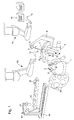
- the arrangement shown in FIG. 1 comprises a turntable 1.
- the turntable 1 there are several brackets 2 (e.g. four brackets 2) provided.
- the brackets 2 are for holding each a dome 4 determined.
- the domes 4 are for this purpose equipped with adapters 3, which are fixed to the brackets 2 can be.
- By turning the turntable 1 a dome 4 aligned with its adapter 3 so that the Dome 4 of a pivotally mounted in a bearing 9 Arm 8 captured and from the turntable 1, i.e. from the brackets 2 out of it, can be removed.
- the arm 8 that with Is pivotable with the help of an engine, on the one hand has one self-centering gripper 7, which is from the hollow (inner) Side of the calotte 4 forth on this in the area of the Dome 4 attached end of the adapter 3 attacks. Outdoors At the end of the arm 8, a clamp 6 is provided which adjusts in this way that it is attached to a free end of the adapter 3 provided rotary bearing 5 attacks.
- there sensors are provided, which the position of the calotte 4 and in particular the nest 4a into which a wafer 19 is inserted or from which a wafer 19 is to be removed.
- the loading spoon 15 serves individual Wafer 19 from a tray 16 and the transfer cylinder 10 to be positively controlled.
- an unloading spoon 12 is provided to the an unloading robot 13 is supported.
- the unloading spoon 12 takes over wafer 19 from the one raised upwards through the nest 4a Transfer cylinder 10 and moves the wafer 19 into one Quartz boat 18, being on the bracket for the quartz boat 18th Sensors 17 (preferably optical / laser sensors) are provided that identify the slot in the quartz boat 18 in the the wafer 19 from the unloading spoon 12 can be used.
- the Laser sensor 17 is along by a displacement device 20 of the quartz boat 18 slidable.
- the spoon 15 provided on the loading robot 14 removes one Wafer 19 from the tray 16 by gripping the back of the wafer.
- the wafer 19 is used by the Principle of holding with a gripper at the same time planarized.
- a station can be provided at which the Wafer flattened, centered and / or, in particular via barcode, be identified. This station can be between the Horde 16 and the loading robot 14 may be provided.
- the side of the wafer 19 to be processed must always be in the nest 4a to the inside of the calotte.
- the loading robot 14 becomes automatic so that the loading spoon 15 with the one to be processed Side of the wafer 19 to the nest 4a to be loaded is aligned. If the loading spoon 15 at the not too processing side of the wafer 19 engages - front side must be processed, it points downwards - the loading spoon lowers 15 and arranges the wafer 19 in the nest 4a of the calotte 4 on. Only then does the loading spoon 15 leave the wafer 19 going on when the one under the nest 4a of the calotte 4 Transfer cylinder 10 the wafer 19 by the Bernoulli principle planarized and stabilized.
- the loading spoon 15 aligned over the nest 4a to be loaded and grabs it on the side of the wafer to be processed 19 becomes the transfer cylinder 10 extended through the nest 4a in the calotte 4 and takes over the wafer 19 from the spoon 15 through the loading spoon 15 provided recesses.
- the loading spoon 15, which is now still between the wafer 19 and the upper end of the transfer cylinder 10 is now, by the loading robot 14th moved out to the side.
- the transfer cylinder 10 is then lowered so that the wafer 19 is arranged in the nest 4a of the calotte 4 becomes. Then the one assigned to the nest 4a Clamping device 100 closed and the wafer 19 in it Nest 4a of the calotte 4 fixed.
- the transfer cylinder 10 moves after the stop functions have been switched off down, and the dome 4 will close to the next one feeding nest 4a rotated. These steps will be continued until all nests of the calotte 4 are loaded with wafers 19 are. Then the dome 4 for further processing the wafer 19 held in it into a work station emotional. For this purpose, the calotte 4 can again be placed on the turntable 1 transferred and in a manner not shown to the processing station after removal from the turntable 1 are fed.
- the dome 4 is put back on the turntable 1, passed from the turntable 1 to the arm 8 and into the in Figure 1 moves, i.e. via their adapter 3 from the self-centering gripper 7 and the clamp 6 held and aligned so that the first nest 4a is facing for unloading the transfer cylinder 10 is arranged.
- the transfer cylinder 10 is with its front end to be removed Wafer 19 approximated, and the wafer 19 is - depending on Process - seized by the transfer cylinder 10 (back process) or planarized / stabilized (front process).
- the clamping device 100 is then opened.
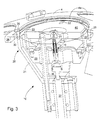
- the transfer cylinder 10, which of the calotte 4 or one Nest 4a thereof for inserting or removing wafers 19 is assigned to the nest 4a, is based on Fig. 3 described in more detail.
- the transfer cylinder 10 consists of an outer, cylindrical Part or cylindrical outer jacket 26, one with this movably connected head 25, which comes from an outer Part 31 and an inner part 28 there.
- guide rods 36 are attached, on which the inner part 28 of the head 25 is slidable and on carry a free device 40 for wafers 19 at their free ends.
- the guide rods 36 are hollow and guide Compressed air for the one located on the holding device 40 Bernoulli ring.
- the inner part 28 of the head 25 with its three reference stops 22 and the one attached in the middle Vacuum head 21 can extend over the nest 4a of the spherical cap 4 will take over a wafer 19 from the loading spoon 15 and drive back into the nest 4a.
- the reference stops 22 or the reference stops 22 themselves can be equipped with a vacuum function his.
- the head 25 of the transfer cylinder 10 is annular (Leaf) spring 30 can be pivoted elastically on the transfer cylinder 10 mounted.
- the transfer cylinder 10 is by moving its cylindrical outer jacket 26 adjustable up and down.
- the transfer cylinder 10 by moving the outer jacket 26 moved upwards via a servomotor 37 until the stops 35 (at least three) on the head 25 on the inside of the Dome 4 abut and thus the holding device 40 of the Head 25 is parallel to the nest 4a of the calotte 4.
- a wafer 19 on the holding device 40 of the transfer cylinder 10 can be planarized in the holding device 40 at least one, preferably annular, nozzle 27 or several nozzle bores aligned at an angle to the plane of the front end be provided, which is pressurized with compressed gas to a wafer 19 by the Bernoulli principle generated forces to the holding device 40 of the transfer cylinder 10 pull and planarize.
- the inner one Part 28 of the head 25 of the transfer cylinder 10 is on the Axes 36 also via an actuator 37, e.g. one Pressure motor or the like, movable up and down, so that the vacuum head 21 and the reference stops 22 through the nest 4a of the dome 4 can be moved around the wafer 19 to take over the corresponding process via the nest 4a or deliver.
- the transfer cylinder 10 is thus by axial adjustment its outer cylinder 26 from the inside against the edge of a Nest 4a moves until the pins 35 abut the edge of the nest 4a and at the same time align the head 25 parallel to the nest 4a.
- the holding device 40 in which the Bernoulli nozzle 27 and the vacuum head 21 is provided, since the latter moves to the Guide rods 36 is attached.
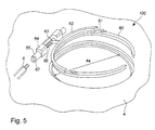
- each nest 4a is in the calottes 4 shows a device 100 for fixing a wafer 19 in the Assigned to nest 4a.
- These clamping devices 100 can, for example the embodiment shown in Figs. 4 and 5 have.
- Round disc 50 provided in all directions is tiltably supported on a swivel arm 51.
- a bolt 52 is attached to the disc 50, which is a double conical hole 53 in the free end of the pivot lever 51 interspersed.
- a spring 54 is provided which between the disc 50 and the free end of the swing arm 51st is arranged.
- the swivel arm 1 can be pivoted about a bearing 56, which is mounted next to the nest 4a on the calotte 4 is.
- drives described in more detail below can be used.
- a substantially round centering plate 57 for example provided such from thin elastic sheet metal, by the spring 54 against a projection 58 on the outside the disc 50 is pressed.
- the elastic centering plate 57 arrives first their downwardly angled edges 59 in contact with the Surrounding area of the nest 4a, so that the disc 50 is parallel is aligned to the nest 4a and thus when closing fully engages in nest level 4b of nest 4a.
- the Swing lever 51 is pivoted so far that spring 52 is slightly compressed so that the disc 50 is elastic against one lying on the edge on the step in the nest 55 Wafer 19 is pressed.
- a clamping ring 60 is provided which elastic connecting means, e.g. Leaf springs 61, at the ends an arc-shaped bracket 62 is attached.
- the Retaining bracket 62 in turn is via a pivot lever 63 and a shaft 65 carrying the pivot lever 63 in a pivot bearing 64 stored.
- a spring 66 is provided, which is biased so that it the clamping ring 60 in its active position, in which a wafer on the step is clamped lying on the edge of the nest 4a, loaded.
- the Clamping ring 60 is in its opposite bearing 64 Interrupted area to allow the movements of a spoon 14, 15 not disabled.
- any tool can be provided be that on the pivot lever 51 or the pivot bracket 61 supporting shaft 65 attacks.
- the Tool provided a polygon that fits into a corresponding Polygonal hole 67 engages in the shaft 65 to the clamping device 100 open.
- FIG. 6 One embodiment for a tool 110 for opening the Clamps 100 is shown in FIG. 6.
- This facility has a motor 70 which drives a polygon 71.
- the motor 70 is connected via two elastic connecting means, e.g. two leaf springs 72, connected to a carrier 73, which in turn over leaf springs 75 that become the first leaf springs 72 are aligned vertically, connected to a holding part 76 is.
- the holding part 76 is with an actuating robot (not shown) coupled.
Landscapes
- Container, Conveyance, Adherence, Positioning, Of Wafer (AREA)
Applications Claiming Priority (2)
| Application Number | Priority Date | Filing Date | Title |
|---|---|---|---|
| DE10056544 | 2000-11-15 | ||
| DE10056544A DE10056544A1 (de) | 2000-11-15 | 2000-11-15 | Verfahren und Vorrichtung zum Be- und Entladen von Halbleiterwafern |
Publications (2)
| Publication Number | Publication Date |
|---|---|
| EP1207548A2 true EP1207548A2 (fr) | 2002-05-22 |
| EP1207548A3 EP1207548A3 (fr) | 2005-11-30 |
Family
ID=7663356
Family Applications (1)
| Application Number | Title | Priority Date | Filing Date |
|---|---|---|---|
| EP01127047A Withdrawn EP1207548A3 (fr) | 2000-11-15 | 2001-11-14 | Méthode et dispositif pour charger et décharger des plaquettes semi-conductrices |
Country Status (2)
| Country | Link |
|---|---|
| EP (1) | EP1207548A3 (fr) |
| DE (1) | DE10056544A1 (fr) |
Cited By (1)
| Publication number | Priority date | Publication date | Assignee | Title |
|---|---|---|---|---|
| US7675606B2 (en) | 2006-05-05 | 2010-03-09 | Asml Netherlands B.V. | Lithographic apparatus and method |
Citations (3)
| Publication number | Priority date | Publication date | Assignee | Title |
|---|---|---|---|---|
| US4457661A (en) | 1981-12-07 | 1984-07-03 | Applied Materials, Inc. | Wafer loading apparatus |
| JPS61220352A (ja) | 1985-03-26 | 1986-09-30 | Seiei Kosan Kk | ウエハ−ロ−デイング装置 |
| US5520501A (en) | 1991-01-25 | 1996-05-28 | Kabushiki Kaisha Toshiba | Wafer holding apparatus |
Family Cites Families (6)
| Publication number | Priority date | Publication date | Assignee | Title |
|---|---|---|---|---|
| JPS5875844A (ja) * | 1981-10-30 | 1983-05-07 | Hitachi Ltd | ウエハ・ハンドリング装置 |
| JP3371002B2 (ja) * | 1992-10-09 | 2003-01-27 | 株式会社トプコン | ウェハの搬送方法 |
| JP2633798B2 (ja) * | 1993-08-26 | 1997-07-23 | シーケーディ株式会社 | 板状部材把持装置 |
| KR100292612B1 (ko) * | 1997-12-08 | 2001-08-07 | 윤종용 | 반도체 웨이퍼 정렬시스템 및 이를 이용하는 웨이퍼 정렬방법 |
| DE19755694C2 (de) * | 1997-12-16 | 2000-05-31 | Sez Semiconduct Equip Zubehoer | Handhabungsvorrichtung für dünne, scheibenförmige Gegenstände |
| DE19921072A1 (de) * | 1999-05-08 | 2000-11-09 | Acr Automation In Cleanroom | Einrichtung zum Handhaben von Substraten innerhalb und außerhalb eines Reinstarbeitsraumes |
-
2000
- 2000-11-15 DE DE10056544A patent/DE10056544A1/de not_active Withdrawn
-
2001
- 2001-11-14 EP EP01127047A patent/EP1207548A3/fr not_active Withdrawn
Patent Citations (3)
| Publication number | Priority date | Publication date | Assignee | Title |
|---|---|---|---|---|
| US4457661A (en) | 1981-12-07 | 1984-07-03 | Applied Materials, Inc. | Wafer loading apparatus |
| JPS61220352A (ja) | 1985-03-26 | 1986-09-30 | Seiei Kosan Kk | ウエハ−ロ−デイング装置 |
| US5520501A (en) | 1991-01-25 | 1996-05-28 | Kabushiki Kaisha Toshiba | Wafer holding apparatus |
Cited By (1)
| Publication number | Priority date | Publication date | Assignee | Title |
|---|---|---|---|---|
| US7675606B2 (en) | 2006-05-05 | 2010-03-09 | Asml Netherlands B.V. | Lithographic apparatus and method |
Also Published As
| Publication number | Publication date |
|---|---|
| EP1207548A3 (fr) | 2005-11-30 |
| DE10056544A1 (de) | 2002-06-06 |
Similar Documents
| Publication | Publication Date | Title |
|---|---|---|
| EP0396923B1 (fr) | Table élévatrice et méthode de transportation | |
| DE19755694C2 (de) | Handhabungsvorrichtung für dünne, scheibenförmige Gegenstände | |
| EP1736279B1 (fr) | Procédé et dispositif de production de verres optiques | |
| DE102020207493B4 (de) | Schneidvorrichtung und verfahren zum wechseln vonverschleissteilen | |
| DE69108908T2 (de) | Vorrichtung zur behandlung einer einzelnen waferscheibe. | |
| DE2423999C3 (de) | Einrichtung zum Ausrichten eines scheibenförmigen Werkstückes in eine vorgegebene Winkellage | |
| DE69302586T2 (de) | Halbleiterwafer transport-modul mit drehbarem und horizontal ausziehbarem halter | |
| DE102016218865B4 (de) | Laserbearbeitungsvorrichtung | |
| EP1402565A2 (fr) | Dispositif de maintien pour des plaquettes de semi-conducteur | |
| DE102007010224B4 (de) | Vorrichtung zum Haltern von scheibenförmigen Objekten | |
| DE3874892T2 (de) | Verfahren und einrichtung zum ausrichten von siliciumplaettchen. | |
| EP0798068B1 (fr) | Dispositif d'usinage d'objets plats, comme par exemple des cartes ou autres documents de type livre | |
| DE2512613C2 (de) | Sauggreifeinrichtung zum Erfassen und Handhaben eines quaderförmigen Körpers | |
| DE102022110462A1 (de) | Vorrichtung und Verwendung zum Blocken einer Linse | |
| DE3723249C1 (de) | Vorrichtung zum Zentrieren und Spannen von Werkstuecken | |
| DE102021214707B4 (de) | Bandanbringer zum anbringen eines bands an einem ringrahmen und einem wafer | |
| EP1207548A2 (fr) | Méthode et dispositif pour charger et décharger des plaquettes semi-conductrices | |
| DE102018105661A1 (de) | Beförderungssystem | |
| DE10113898A1 (de) | Einrichtung zum Zuführen und/oder Wegführen von mit Objekten gefüllten Magazinen | |
| DE10007389B4 (de) | Vorrichtung zur Entnahme von Halbleiterscheiben aus Läuferscheiben in einer doppelseitigen Poliermaschine | |
| DE2930026A1 (de) | Einrichtung zum aufbringen von abdichtmaterial auf eine abdichtflaeche eines trichterfoermigen kolbenteils einer kathodenstrahlroehre | |
| DE69211998T2 (de) | Positionier-und kupplungvorrichtung eines antriebs | |
| DE10161902B4 (de) | Verfahren und Vorrichtung zum Handhaben von Platten | |
| EP4247598B1 (fr) | Dispositif de préhension et manipulateur doté d'un dispositif de préhension | |
| EP1294014B1 (fr) | Dispositif de manipulation de plaques |
Legal Events
| Date | Code | Title | Description |
|---|---|---|---|
| PUAI | Public reference made under article 153(3) epc to a published international application that has entered the european phase |
Free format text: ORIGINAL CODE: 0009012 |
|
| AX | Request for extension of the european patent |
Free format text: AL;LT;LV;MK;RO;SI |
|
| RIN1 | Information on inventor provided before grant (corrected) |
Inventor name: KERHE, MARIAN Inventor name: MATSCHITSCH, MARTIN Inventor name: KROUPA, GERHARD Inventor name: GOLUBIC, RICHARD Inventor name: GIOVANNINI, ALBERTO Inventor name: FERTSCHEI, ANNEMARIE Inventor name: BINDER, ALFRED Inventor name: AIGNER, KURT |
|
| PUAL | Search report despatched |
Free format text: ORIGINAL CODE: 0009013 |
|
| AK | Designated contracting states |
Kind code of ref document: A3 Designated state(s): AT BE CH CY DE DK ES FI FR GB GR IE IT LI LU MC NL PT SE TR |
|
| AX | Request for extension of the european patent |
Extension state: AL LT LV MK RO SI |
|
| 17P | Request for examination filed |
Effective date: 20060127 |
|
| AKX | Designation fees paid |
Designated state(s): AT DE FR GB IT |
|
| 17Q | First examination report despatched |
Effective date: 20080122 |
|
| RAP1 | Party data changed (applicant data changed or rights of an application transferred) |
Owner name: INFINEON TECHNOLOGIES AG |
|
| GRAP | Despatch of communication of intention to grant a patent |
Free format text: ORIGINAL CODE: EPIDOSNIGR1 |
|
| RIN1 | Information on inventor provided before grant (corrected) |
Inventor name: ZERLAUTH, STEFAN Inventor name: WOEHLERT, STEFAN Inventor name: UNTERWEGER, JOSEF Inventor name: SCHERF, WERNER Inventor name: RUDOLF, CONNY-NORBERT Inventor name: MANZONI, GIULIO Inventor name: LADINIG, MARCELLO Inventor name: KERHE, MARIAN Inventor name: MATSCHITSCH, MARTIN Inventor name: KROUPA, GERHARD Inventor name: GOLUBIC, RICHARD Inventor name: GIOVANNINI, ALBERTO Inventor name: FERTSCHEI, ANNEMARIE Inventor name: BINDER, ALFRED Inventor name: AIGNER, KURT |
|
| STAA | Information on the status of an ep patent application or granted ep patent |
Free format text: STATUS: THE APPLICATION IS DEEMED TO BE WITHDRAWN |
|
| 18D | Application deemed to be withdrawn |
Effective date: 20101222 |