EP1207587A2 - Connecteur à haute fréquence pour bord de plaquette à circuits imprimés - Google Patents
Connecteur à haute fréquence pour bord de plaquette à circuits imprimés Download PDFInfo
- Publication number
- EP1207587A2 EP1207587A2 EP01126526A EP01126526A EP1207587A2 EP 1207587 A2 EP1207587 A2 EP 1207587A2 EP 01126526 A EP01126526 A EP 01126526A EP 01126526 A EP01126526 A EP 01126526A EP 1207587 A2 EP1207587 A2 EP 1207587A2
- Authority
- EP
- European Patent Office
- Prior art keywords
- connector
- modules
- module
- array
- connector module
- Prior art date
- Legal status (The legal status is an assumption and is not a legal conclusion. Google has not performed a legal analysis and makes no representation as to the accuracy of the status listed.)
- Withdrawn
Links
Images








Classifications
-
- H—ELECTRICITY
- H01—ELECTRIC ELEMENTS
- H01R—ELECTRICALLY-CONDUCTIVE CONNECTIONS; STRUCTURAL ASSOCIATIONS OF A PLURALITY OF MUTUALLY-INSULATED ELECTRICAL CONNECTING ELEMENTS; COUPLING DEVICES; CURRENT COLLECTORS
- H01R12/00—Structural associations of a plurality of mutually-insulated electrical connecting elements, specially adapted for printed circuits, e.g. printed circuit boards [PCB], flat or ribbon cables, or like generally planar structures, e.g. terminal strips, terminal blocks; Coupling devices specially adapted for printed circuits, flat or ribbon cables, or like generally planar structures; Terminals specially adapted for contact with, or insertion into, printed circuits, flat or ribbon cables, or like generally planar structures
- H01R12/70—Coupling devices
- H01R12/71—Coupling devices for rigid printing circuits or like structures
-
- H—ELECTRICITY
- H01—ELECTRIC ELEMENTS
- H01R—ELECTRICALLY-CONDUCTIVE CONNECTIONS; STRUCTURAL ASSOCIATIONS OF A PLURALITY OF MUTUALLY-INSULATED ELECTRICAL CONNECTING ELEMENTS; COUPLING DEVICES; CURRENT COLLECTORS
- H01R12/00—Structural associations of a plurality of mutually-insulated electrical connecting elements, specially adapted for printed circuits, e.g. printed circuit boards [PCB], flat or ribbon cables, or like generally planar structures, e.g. terminal strips, terminal blocks; Coupling devices specially adapted for printed circuits, flat or ribbon cables, or like generally planar structures; Terminals specially adapted for contact with, or insertion into, printed circuits, flat or ribbon cables, or like generally planar structures
- H01R12/70—Coupling devices
- H01R12/71—Coupling devices for rigid printing circuits or like structures
- H01R12/72—Coupling devices for rigid printing circuits or like structures coupling with the edge of the rigid printed circuits or like structures
- H01R12/721—Coupling devices for rigid printing circuits or like structures coupling with the edge of the rigid printed circuits or like structures cooperating directly with the edge of the rigid printed circuits
-
- H—ELECTRICITY
- H01—ELECTRIC ELEMENTS
- H01R—ELECTRICALLY-CONDUCTIVE CONNECTIONS; STRUCTURAL ASSOCIATIONS OF A PLURALITY OF MUTUALLY-INSULATED ELECTRICAL CONNECTING ELEMENTS; COUPLING DEVICES; CURRENT COLLECTORS
- H01R13/00—Details of coupling devices of the kinds covered by groups H01R12/70 or H01R24/00 - H01R33/00
- H01R13/648—Protective earth or shield arrangements on coupling devices, e.g. anti-static shielding
- H01R13/658—High frequency shielding arrangements, e.g. against EMI [Electro-Magnetic Interference] or EMP [Electro-Magnetic Pulse]
- H01R13/6581—Shield structure
- H01R13/6585—Shielding material individually surrounding or interposed between mutually spaced contacts
Definitions
- the present invention relates to modular electrical connectors and, more particularly, to card edge connectors with modular inserts.
- Electrical connectors assembled from a plurality of connector modules are well known in the art.
- Card edge connectors for connecting an edge of a printed circuit board to another electronic component are also well known in the art.
- an electrical connector comprising a frame, at least one first connector module and at least one different second connector module.
- the frame has at least one connector module receiving area adapted to receive a plurality of connector modules.
- the frame comprises a first array of connector module locating features and a different second array of connector module locating features.
- the first connector module is located in the at least one receiving area.
- the first connector module has a housing and electrical contacts.
- the first connector module comprises a mating first array of positioning features interlocked with at least a portion of the first array of locating features in the frame.
- the different second connector module is located in the at least one receiving area.
- the second connector module has a housing and electrical contacts.
- the second connector module comprises a mating different second array of positioning features interlocked with at least a portion of the second array of locating features in the frame.
- an electrical connector comprising a frame, at least one first connector module located in a first receiving area of the frame, and at least one second connector module or first connector module located in a second receiving area of the frame.
- the frame has a first connector module receiving area and a spaced second connector module receiving area. Each receiving area is adapted to receive at least two connector modules.
- the second receiving area is adapted to receive at least two different connector modules.
- the at least one first connector module is located in the first receiving area.
- the at least one second connector module or first connector module is located in the second receiving area.
- the connector can be provided with connector modules in the second receiving area with or without the second connector modules.
- a method of assembling an electrical connector comprising steps of providing a frame having a connector module receiving area; selecting at least two connector modules from a plurality of different types of connector modules, each connector module having a housing and an electrical contact; and inserting the selected connector modules into the same receiving area adjacent each other, wherein the connector modules and the frame in the receiving area comprise interlocking locating features to stationarily mount the housings to the frame.
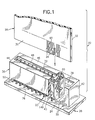
- FIG. 1 there is shown an exploded perspective view of a card edge connector assembly 20 incorporating features of the present invention.
- the present invention will be described with reference to the embodiments shown in the drawings, it should be understood that the present invention can be embodied in many alternate forms of embodiments. In addition, any suitable size, shape or type of elements or materials could be used.
- the card edge connector assembly 20 mounts to a plurality of contact pads 22 arranged in a contact pattern 23 on an underlying contact surface 24 in the form of a motherboard 26, for example.
- a planar card 28, a daughter board, for example, has first and second opposed surfaces 30, 32 with conductive contact members 34 on at least one of the opposed surfaces.
- an elongated longitudinally extending outer frame 36 defines a reception region 38 which is adapted to receive a plurality of modules 40.
- Each of the modules 40 includes contact members (to be described below) and the modules lie side by side in parallel laterally extending planes which, as an assembly, are positioned to connectively engage with the mating contact pads 22 on the underlying contact surface 24.
- the outer frame 36 includes opposed spaced end walls 42, opposed spaced side walls 44, and a top wall 46 integrally joining the end walls and the side walls.
- the end walls, side walls, and top wall together define the reception region 38, the top wall having a longitudinally extending aperture 48.
- the end walls 42 and the side walls 44 extend to a lower rim 50 distant from the top wall 46 and define, interiorly, an opening 52 through which the modules are inserted into the reception region 38.
- each module 40 includes an insulative housing 54 which has first and second spaced generally parallel elongated passages 56, 58 therein and a card receiving recess 60 for reception of the planar card 28 (Fig. 1) between the first and second passages.
- a first elongated contact 62 is firmly received in a known manner in the first passage 56 and has a first contact surface 64 positioned for engagement with an associated contact pad 22 (Fig. 1) on the contact pattern 23 of the underlying contact surface 24 using known techniques.
- a second elongated contact 66 is firmly received in the second passage 58 having a first contact surface 68 positioned for engagement with another associated contact pad 22 on the contact pattern 23 of the underlying contact surface 24.
- any type of termination e.g. press-fit, pin-in-paste
- any type of termination could be used.
- the card receiving recesses 60 of the plurality of modules 40 integrated as a group within the outer frame 36 define a longitudinally extending card receiving slot 70.
- the first elongated contact 62 includes a second contact surface 72 projecting into the card receiving slot 70 (or recess 60 of an individual module 40).
- the second contact surface 72 engages with an associated conductive contact member 34 on the first surface 30 of the planar card 28 inserted into the card receiving slot.
- the second elongated contact 66 includes a second contact surface 74 projecting into the card receiving slot 70 (or recess 60 of an individual module 40) in the direction of the first elongated contact 62. This time, the second contact surface 74 engages with a second one of the conductive contact members 34, this one being on the second surface 32 of the planar card 28 inserted into the card receiving slot.
- the lower rim 50 of the outer frame 36 includes a cutout region 76 enabling visual inspection of the first contact surfaces 64, 68 of the first and second elongated contacts 62, 66 when engaged with their associated contact pads, respectively. Also, aperture 48 of the outer frame 36 is aligned with the card receiving slot 70 when the plurality of modules are received in the reception region 38.
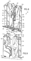
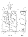
- Figs. 9, 10, and 11 which illustrate opposed ground shields 78, 80, each having a C-shaped cross section for slidable reception, respectively, on an outer peripheral surface 82 of the insulative housing.
- the ground shields 78, 80 are positioned in opposed relationship and in proximate engagement with the outer peripheral surface 82.
- the first ground shield 78 generally overlies the first elongated passage 56 and the second ground shield 80 generally overlies the second elongated passage 58.
- the ground shields 78, 80 both include a first integral ground contact 84 for engagement (Fig. 1) with an associated ground contact or pad 86 of an external unit such as the mother board 26.
- each of the ground shields 78, 80 includes a second integral ground contact 88 for engagement with an associated ground contact surface 90 on the planar card 28 inserted into the card receiving slot 70. As seen especially well in Figs. 9, 10, and 11, each of the ground shields 78, 80 has a cutout region 92.
- the cutout region 92 enables visual inspection of the first contact surfaces 64, 68 of the first and second elongated contacts 62, 66 when engaged with their associated mating contact pads 22, respectively, and of the first and second ground contacts 84 when engaged with their respective mating ground contact pads 86 of the external unit or motherboard 26.
- the outer peripheral surface 82 of the insulative housing 54 has first and second opposed major sides 94, 96, respectively, and a first minor side 98 joining the first and second major sides.
- the outer peripheral surface 82 of the insulative housing 54 has third and fourth opposed major sides 100, 102 and a second minor side 104 joining the first and second major sides.
- the first and third major sides 94, 100 are coplanar and the second and fourth major sides 96, 102 are coplanar.
- the first and second minor sides 98, 104 lie in parallel spaced apart planes.
- the insulative frame 54 also has a first elongated slot 106 spaced from and aligned with the card receiving recess 60 and having an inlet positioned intermediate the first and third major sides, 94, 100.
- the first elongated slot 106 is generally parallel with the first and second minor sides 98, 104.
- the insulative frame 54 also has a second elongated slot 107, also spaced from and aligned with the card receiving recess 60 and having an inlet positioned intermediate the second and fourth major sides 96, 102, respectively.
- the second elongated slot 107 is generally parallel with the first and second minor sides 98, 104 and coplanar with the first elongated slot 106.
- a complete module 40 includes, as earlier described in a more general description, the first and second ground shields 78, 80, and these will now be described more completely as they are mounted on the insulative housing 54.
- Each ground shield 78, 80 has a C-shaped cross section and has earlier been described as being slidably received on the insulative housing in opposed relationship and in proximate engagement with the outer peripheral surface 82.
- the first ground shield 78 generally overlies the first elongated passage 56 and the second ground shield 80 generally overlies the second elongated passage 58.
- the first ground shield 78 has first and second opposed limbs 108, 110 proximately overlying the first and second major sides 94, 96, respectively, and a first side limb 112 proximately overlies the first minor side 98.
- a first flange limb 114 extends transverse of the first opposed limb 108 and is slidably received in the first elongated slot 106. With this construction, the first ground shield 78 substantially completely surrounds the first elongated contact 62 received in the first elongated passage 58.
- the second ground shield 80 has third and fourth opposed limbs 116, 118 proximately overlying the third and fourth major sides 100, 102, respectively.
- a second side limb 120 proximately overlies the second minor side 104.
- a second flange limb 122 extends transverse of the third opposed limb 116 and is slidably received in the second elongated slot 107.
- first and second ground shields 78, 80 both include a first integral downwardly projecting ground contact 84 for engagement with a mating ground contact or pad 86 of an external unit such the motherboard 26.
- the mating ground contact or pad 86 is associated with the mating contacts 22 engaged by the first contact surfaces 64, 68 of the first and second elongated contacts 62, 66.
- each of the first and second ground shields 78, 80 includes a second integral ground contact 88 for engagement with an associated ground contact surface 90 on the planar card 28 inserted into the card receiving slot 60.
- both of the second integral ground contacts 88 of the first and second ground shields 78, 80 project into the card receiving recess 60, with the ground contact 88 of the first ground shield 78 generally facing the ground contact 88 of the second ground shield 80.
- each of the second integral ground contacts 88 of the first and second ground shields project into the card receiving recess 60 at a location nearer the top wall 46 of the outer frame 36 than either of the second contact surfaces 72, 74 of the first and second elongated contacts 62, 66. In this manner, an early mate, late break, grounding operation can be established. More specifically, this construction serves to establish in a preemptive manner common electrical grounding across the contact interface in advance of other electrical interconnection of the first and second electrical contacts 62, 66.
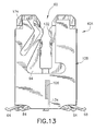
- a single tubular ground shield 128 is slidably received on the insulative housing in proximate engagement with the outer peripheral surface 82.
- the tubular ground shield 128 includes a first pair of integral ground contacts 130, each provided for engagement with a ground contact 86 (Fig. 1) of an external unit or motherboard 26 associated with the mating contacts engaged by the first contact surfaces of the first and second elongated contacts 62, 66.
- the tubular ground shield 128 also includes a second pair of integral ground contacts 132 for engagement with the ground contact surfaces 90 (see Fig. 1) on the planar card 28 inserted into the card receiving slot 70 of the insulative housing 54.
- the tubular ground shield 128 operates in the manner of the pair of opposed ground shields 78, 80.
- This includes the provision of a pair of flange limbs 134, similar to the flange limbs 122, which are mutually opposed and coplanar and are slidably received in the second elongated slots 106, 107 of the insulative housing 54.
- the ground shield 128 substantially completely surrounds each of the elongated contacts 62, 66 received in the passages 56, 58.
- the insulative housing 54 is formed with first and second spaced pairs of generally parallel elongated passages therein 56 and 56A and 58 and 58A with an elongated contact firmly received in each in the manner previously described.
- each elongated contact has first and second contact surfaces with the construction previously described for mating contact with associated contact surfaces on the motherboard 26 and on the planar card 28.
- the outer frame may be provided with a variety of locating features at a plurality of longitudinally spaced locations.
- the top wall 46 is provided with a plurality of laterally extending protrusions 136 projecting into the reception region 38 which engage associated modules 40 and maintain them in a spaced side-by-side relationship. In this instance, the spacing between each pair of protrusions is approximately equal to the thickness of a module and adjacent modules are maintained a slight distance apart.
- Similar constructions are illustrated in Figs. 15 and 16.
- a plurality of similarly spaced upright protrusions 138 are provided on the inside surfaces of the side walls 44.
- Fig. 14 a plurality of similarly spaced upright protrusions 138 are provided on the inside surfaces of the side walls 44.
- a plurality of similarly spaced corner protrusions 140 are provided at the inner interface between the side walls 44 and top wall 46.
- the protrusions 136 or 138 or 140 repeat at the same pitch distances for the entire length of the outer frame 36.
- each module has complimentary locating features formed for engagement with locating features of the outer frame, again, such that each module is positively positioned with respect to the outer frame.
- lateral protrusions 142 are illustrated which may be of the nature and longitudinal spacing of the protrusions 136.
- modified modules 40A have a laterally extending groove 144 which matingly receives the lateral protrusions 142 to maintain the modules in a spaced side-by-side relationship with adjacent modules maintained a slight distance apart.
- downwardly extending protrusions 146 are appropriately located to project into the uppermost end portions of the elongated passages 56, 56A, 58, and 58A of the insulative housing 54.
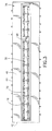
- This construction is also seen, for example, in Fig. 2.
- the modules are maintained in a spaced side-by-side relationship with adjacent modules maintained a slight distance apart.
- a septum member 148 may be provided intermediate the spaced end walls 42 and lying in a plane parallel to the end walls. With this construction, the reception region 38 is separated into first and second chambers 150, 152 (Fig 2) for receiving the modules 40.
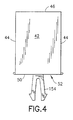
- a retention clip 154 may be attached to the septum member 148 at the lower rim, extending away from the outer frame 36 in a direction away from the top wall 46.
- a plurality of retention clips 154 may be provided for attaching the outer frame 36 to an underlying surface, for example, to the motherboard 26, one of the retention clips mounted on each end wall 42 and on each septum member 148 at the lower rim 50.
- the retention clip extends in a direction away from the top wall 46 and are secured to the substrate with known techniques.
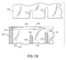
- a modified outer frame 36A is illustrated in which a pair of longitudinally spaced septum members 156, 158 are provided intermediate the spaced end walls 42A.
- the septum members 156, 158 lie in planes parallel to the end walls 42A and thereby separate the reception region 38A into a plurality of chambers 160, 162, 164 for receiving the modules 40.
- Each of the septum members 156, 158 includes a registration feature, for example, uppermost edges 166, 168 enabling a modified planar card 28A with conductive contact members thereon (not shown) and complementary registration features 170, 172 to be fully inserted through the longitudinally extending aperture of the top wall 46A and into the card receiving slot.
- the slotted registration features 170, 172 are positioned and sized for engageable reception, first of the uppermost edges 166, 168, respectively, then the remainder of the septum members 156, 158 so that, in turn, the conductive contact members on the planar card 28A can be mechanically and electrically engaged by the second elongated contact surfaces of the elongated contacts 62, 66 of the plurality of modules.
- planar card 28A does not possess the registration features 170, 172 positioned and sized to receive the septum members 156, 158, the planar card would be rejected and incapable of use with the system of the invention.
- the modules 40 When the modules 40 are arranged in side-by-side fashion within the outer frame 36, it may be desirable to provide some further instrumentality, other than those already described, to keep adjacent modules at spaced distances apart. This can be achieved, for example, by providing at least one boss member 174, and preferably several at spaced apart locations on the outer peripheral surface 82 of one insulative housing 54 of a module 40 such that it is, or they are, engageable with the insulative housing of an adjoining module. See Fig. 2. The boss member would be dimensioned to prevent mutual engagement of the ground shield 128 or ground shields 78, 80 of the adjoining modules.
- a plurality of mutually opposed pairs of boss members 176, 178 may be provided on the insulative housings of adjoining modules.
- the mutually opposed pairs of boss members are aligned for engagement and dimensioned to prevent mutual engagement of the ground shields of the adjoining modules.
- a bridging contact 180 may be provided on at least one of the ground shields of one of the members 40 engageable with the ground shield of its adjoining member.
- FIG. 20 there is shown a partial top and longitudinal side perspective view of an alternate embodiment of an electrical connector 200, with a cut-away section, which is attached to a printed circuit board 202.
- a portion of the top 206 of the housing frame 204 of the connector 200 is shown cut-away from the card edge receiving slot 208 back to one side wall 210.
- the connector 200 generally comprises the housing frame 204 and connector modules or modules 212, 214, 216 connected to the frame 204.
- the modules 212, 214, 216 comprise modules from two different families of modules. However, more or less than two families of modules could be provided.
- each family of modules could comprise only one or more than one type of different modules as explained in further detail below.
- the frame 204 comprises two module receiving areas 218, 220. However, more or less than two module receiving areas could be provided. In this embodiment the two module receiving areas 218, 220 are separated from each other by a portion 222 of the frame which also comprises a septum member 224. However, any suitable separation could be provided.
- the first receiving area 218 includes a first array of connector module location features 226.
- the locating features 226 comprise inward projections along the side walls 210, 211. In alternate embodiments the locating features could comprise recesses and/or could extend downward from the top 206 into the receiving area 218.
- the first receiving area 218 could also comprise more than one array of locating features.
- the second receiving area 220 includes a second array of connector module locating features 226.
- the locating features in the second area 220 are the same as the locating features in the first area 218. However, in an alternate embodiment they could be different.
- the centerline spacing S between adjacent locating features 226 is also the same in both receiving areas 218; 220, but could be different.
- the first family of modules in the embodiment shown, comprise the two different types of modules 212, 214. However, the first family could comprise merely one type of module or more than two types of modules. In this embodiment both types of modules in the first family comprise a same housing 228 and same signal contacts 230. However, in alternate embodiments the housings and/or signal contacts for the different types of modules in the first family of modules could be different.
- Each housing 228 has an array of positioning features 232 which interlock with at least a portion of the first array of gonc features 226 in the frame 204. In this embodiment the positioning features 232 comprise grooves or recesses along opposite side walls of the housing 228; one on each side wall.
- any suitable array could be provided and the positioning features could have any suitable shape so long as they interlockingly mate with locating features on the frame.
- the difference between the two types of modules 212 and 214 of the first family is the presence or absence of a ground shield.
- the first type of modules 212 comprise ground shields 234 substantially identical to the shields 128 shown in Fig. 12, but the shields 234 can have slots to accommodate the mating locating features 226 and positioning features 232.
- the second type of modules 214 do not comprise ground shields. In alternate embodiments other features could differentiate the two types of modules 212, 214.
- the shields 234 of adjacent first type of modules 212 can be formed as differential pair signal and ground contacts for high speed signal transmission.
- the contacts 230 in the second type of module 214 could merely be ordinary signal contacts for slower speed signal transmission.
- the first and second types of modules 212, 214 could be intermixed or arranged in any suitable pattern in the first receiving area 218.
- the second family of modules in the embodiment shown, merely comprises one third type of module 216.
- the second family of modules could comprise more than one type module having, for example, different housings, and/or contacts, and/or shielding.
- the connector 200 merely comprises two of the modules 216, but more or less could be provided.
- Each module 216 has a housing 236 and contacts 238.
- the housings 236 each comprise an array of positioning features 240 which interlock with at least a portion of the second array of locating features 226 in the second receiving area 220.
- the positioning features 240 comprise grooves or recesses along opposite side walls of the housing 236; two on each side.
- any suitable array could be provided and the positioning features could have any suitable shape.
- the modules 216 do not comprise shielding and are not intended for high speed signal transmission.
- the first receiving area 218 can have modules from the first family of modules which are separate from the second receiving area 220.
- the second receiving area 220 can have modules from the second family of modules.
- the two families of modules are differentiated from each other by their different housings 228 and 236.
- the differentiation among families of modules could be based upon additional features or alternative features.
- the housings could have different positioning features or different types of contacts.
- One of the features of the present invention is the ability to configure the types of modules which are located in the first receiving area 218 from a selection of different types of modules in a first family of modules and, the ability for configuration or patterning of the different types of modules from a same family in the same receiving area. For example, only modules 212, only modules 214, or mixtures of modules 212 and 214 could be provided in the first receiving area 218.
- FIG. 20 shows the connector 200 with modules from two families of modules.
- the connector could alternatively be configured to have modules from only the first family of modules; i.e., without using the modules 216.
- the modules 212 or 214 could be located in the second receiving area 220. This is because the locating features 226 in the first and second receiving areas have the same size and spacing, such that the positioning features 232 can work in the second receiving area.
- length of the housing 236 is a multiple of the length of the housing 228. In this embodiment the length multiple is 2, however, any suitable multiple could be used. Therefore, in this embodiment, each of the modules 216 can be replaced by two of the modules 212 and/or 214.
- FIG. 21 shows a schematic bottom plan view of a housing frame 250 for an electrical connector, for example a card edge connector.
- the frame 250 has three connector module receiving areas 252, 254, 256.
- the first receiving area 252 has a main section 258 and a first array of a first type of locating features 260.
- the second receiving area 254 has a main section 262 and a second array of a second type of locating features 264.
- the third receiving area 256 has a main section 266 and a third array of locating features comprising a mixture or combination of the arrays of first and second types of locating features 260 and 264.
- the locating features 258, 264 and 268 comprise grooves in the inside surfaces of the side walls 270, 272 of the frame 250.
- any suitable locating features could be provided.
- a first family of connector modules for use with the frame 250 are shown in Figs. 22a-22c.
- the first family of modules comprises three different types of modules 274, 276, 278.
- the first module 274 has a first type of housing 280 and first contacts 282.
- the first housing 280 has positioning features 284 for positioning in a portion of the first array of locating features 260.
- the first contacts 282 are preferably signal contacts located in two groups 286, 288 with different contact pitches.
- the module 276 has a second housing 290 and first contacts 282.
- the second housing 290 has a same length as the first housing 280 and a same pattern of the locating features 260, but has a different contact pitch (only the pitch equivalent to group 288) for its contacts 282.
- the third module 278 has a housing 292 with a longer length than the housings 280 and 290, but has a same repeating pattern for its positioning features 284 and only one contact pitch for its contacts 282.
- the third housing 292 is sized and shaped to substantially precisely fit inside the first receiving area 252.
- two of the first and/or second types of modules 274, 276 could be located in the first receiving area 252.
- the first family of connector modules could have different housing lengths and contact positions, but in this embodiment they can all be identified by the size, shape and relative positioning of their positioning features 284.
- the second family of connector modules for use with the frame 250 are shown in Figs. 23a-23b.
- the second family of modules comprises three different types of modules 294, 296, 298.
- the first module 294 has a first type of housing 300 and second contacts 302.
- the first housing 300 has positioning features 304 for position in a portion of the second array of locating features 264.
- the second contacts are preferably power contacts.
- the second module 296 has a second housing 306 and a third type of contact 308.
- the second housing 306 has a same length as the first housing 300 and a same pattern to the position features 304, but merely has a different size and shape hole for the contact 308.
- the contact is preferably a power contact, but has a different shape from the power contacts 302.
- the third module 298 has a housing 310 with a longer length than the housings 300 and 306, but has a same repeating pattern for its positioning features 304.
- the third module 298 has both the first and second types of power contacts 302 and 308.
- Other members of the second type of family could also be provided, such as having different contacts, housing lengths, or other variations, but they can all be identified by the size, shape and relative positioning of their positioning features 304.
- Combinations of modules 294 and/or 296 and/or 298 can be used to fill in the second receiving area 254 in the frame 250.
- the locating features 260 in the first receiving area 252 and the locating features 264 in the second receiving area 254 are configured to receive modules from only the first family of connector modules and the second family of connector modules, respectively.
- the connector modules 294-298 of the second family cannot be inserted into the first receiving area 252 because of the differences between locating features 260 and positioning features 304.
- the connector modules 274-278 of the first family cannot be inserted into the second receiving area 254 because of the differences between the locating features 264 and the positioning features 284.
- the third receiving area 256 is adapted to receive modules from both of the module families. In alternate embodiments the third receiving area might not be provided, or more than one third receiving area could be provided or, one or both of the first and second receiving areas might not be provided. In the embodiment shown, the right side of the third area 256 could receive two of the modules 294 and/or 296. The left side and center of the third area 256 could receive modules 274, 276 and/or 278. In addition, the right side of the third area 256, and/or the center and right side of the area 256, might include one or more of the first- family of modules.
- the present invention can allow for a connector frame to be able to receive heterogeneous groups of modular units ( s) of sets of various designs and purposes (families) to form electrical connectors.
- the connector frame can comprise locating features designed to selectively admit subset combinations of families in some predetermined locations while rejecting these subsets in favor of other subsets from a different family.
- the assembly can comprise subassemblies of identical shielded modular units which can be interspersed with lower cost non-shielded units and/or special-purpose units (such as for high current interconnections). Some positions in the frame could be left blank or could be filled with blank or dummy modules.
- Sets of frames and modules may be designed with distinct families of position structures and features, whereby these frames, in offering a first set of positioning structures in any one aperture and a mechanically incompatible second and distinct series of positioning structures in any other aperture will prevent the mingling of one family of module designs with a second family of designs within the same aperture.
- This segregation may be advantageous as a polarity feature, or as a means of eliminating assembly operator error, or to provide a special and proprietary series of product distinct from a general commodity design.
- An additional advantage of such segregation is the separation and deliberate location of a distinct series of modules of an especially robust design capable of withstanding severe service, such as high voltages, high currents, or exceptional mating life demands, whose special positioning structures are mechanically incompatible with elements from the series of standard service designs.
- severe service such as high voltages, high currents, or exceptional mating life demands
- segregation can advantageously prevent an undesirable or dangerous condition, including the untimely or catastrophic failure of any improperly positioned standard service unit or group accidentally subjected to severe service.
Landscapes
- Connector Housings Or Holding Contact Members (AREA)
- Details Of Connecting Devices For Male And Female Coupling (AREA)
- Coupling Device And Connection With Printed Circuit (AREA)
- Manufacturing Of Electrical Connectors (AREA)
Applications Claiming Priority (2)
| Application Number | Priority Date | Filing Date | Title |
|---|---|---|---|
| US712704 | 1985-03-15 | ||
| US71270400A | 2000-11-14 | 2000-11-14 |
Publications (2)
| Publication Number | Publication Date |
|---|---|
| EP1207587A2 true EP1207587A2 (fr) | 2002-05-22 |
| EP1207587A3 EP1207587A3 (fr) | 2003-10-15 |
Family
ID=24863197
Family Applications (1)
| Application Number | Title | Priority Date | Filing Date |
|---|---|---|---|
| EP01126526A Withdrawn EP1207587A3 (fr) | 2000-11-14 | 2001-11-13 | Connecteur à haute fréquence pour bord de plaquette à circuits imprimés |
Country Status (4)
| Country | Link |
|---|---|
| EP (1) | EP1207587A3 (fr) |
| JP (1) | JP2002222674A (fr) |
| KR (1) | KR20020037690A (fr) |
| CA (1) | CA2361875A1 (fr) |
Cited By (20)
| Publication number | Priority date | Publication date | Assignee | Title |
|---|---|---|---|---|
| CN105191003A (zh) * | 2013-03-13 | 2015-12-23 | 安费诺有限公司 | 用于高速电连接器的壳体 |
| US10461467B2 (en) | 2017-01-20 | 2019-10-29 | Fci Usa Llc | Compact card edge connector |
| US10651603B2 (en) | 2016-06-01 | 2020-05-12 | Amphenol Fci Connectors Singapore Pte. Ltd. | High speed electrical connector |
| US10720735B2 (en) | 2016-10-19 | 2020-07-21 | Amphenol Corporation | Compliant shield for very high speed, high density electrical interconnection |
| US10840649B2 (en) | 2014-11-12 | 2020-11-17 | Amphenol Corporation | Organizer for a very high speed, high density electrical interconnection system |
| US10931062B2 (en) | 2018-11-21 | 2021-02-23 | Amphenol Corporation | High-frequency electrical connector |
| US11070006B2 (en) | 2017-08-03 | 2021-07-20 | Amphenol Corporation | Connector for low loss interconnection system |
| US11101611B2 (en) | 2019-01-25 | 2021-08-24 | Fci Usa Llc | I/O connector configured for cabled connection to the midboard |
| US11189943B2 (en) | 2019-01-25 | 2021-11-30 | Fci Usa Llc | I/O connector configured for cable connection to a midboard |
| US11205877B2 (en) | 2018-04-02 | 2021-12-21 | Ardent Concepts, Inc. | Controlled-impedance compliant cable termination |
| US11437762B2 (en) | 2019-02-22 | 2022-09-06 | Amphenol Corporation | High performance cable connector assembly |
| US11444398B2 (en) | 2018-03-22 | 2022-09-13 | Amphenol Corporation | High density electrical connector |
| US11469554B2 (en) | 2020-01-27 | 2022-10-11 | Fci Usa Llc | High speed, high density direct mate orthogonal connector |
| US11522310B2 (en) | 2012-08-22 | 2022-12-06 | Amphenol Corporation | High-frequency electrical connector |
| US11670879B2 (en) | 2020-01-28 | 2023-06-06 | Fci Usa Llc | High frequency midboard connector |
| US11735852B2 (en) | 2019-09-19 | 2023-08-22 | Amphenol Corporation | High speed electronic system with midboard cable connector |
| USD1002553S1 (en) | 2021-11-03 | 2023-10-24 | Amphenol Corporation | Gasket for connector |
| US11799246B2 (en) | 2020-01-27 | 2023-10-24 | Fci Usa Llc | High speed connector |
| US11831106B2 (en) | 2016-05-31 | 2023-11-28 | Amphenol Corporation | High performance cable termination |
| US12051867B2 (en) | 2020-12-04 | 2024-07-30 | Amphenol Commercial Products (Chengdu) Co., Ltd. | Card edge connector with a locking system |
Families Citing this family (1)
| Publication number | Priority date | Publication date | Assignee | Title |
|---|---|---|---|---|
| JP7417842B2 (ja) * | 2020-09-09 | 2024-01-19 | 株式会社オートネットワーク技術研究所 | 表面実装コネクタ |
Family Cites Families (4)
| Publication number | Priority date | Publication date | Assignee | Title |
|---|---|---|---|---|
| JP3415889B2 (ja) * | 1992-08-18 | 2003-06-09 | ザ ウィタカー コーポレーション | シールドコネクタ |
| US5538435A (en) * | 1994-09-14 | 1996-07-23 | The Whitaker Corporation | Electrical input/output connector with switchable contacts |
| US5924898A (en) * | 1997-05-29 | 1999-07-20 | Raychem Corporation | Modular connector |
| DE29803738U1 (de) * | 1998-03-04 | 1999-07-01 | Karl Lumberg GmbH & Co, 58579 Schalksmühle | Führungsrahmen für direkte Steckverbinder |
-
2001
- 2001-11-09 CA CA002361875A patent/CA2361875A1/fr not_active Abandoned
- 2001-11-13 JP JP2001347440A patent/JP2002222674A/ja active Pending
- 2001-11-13 KR KR1020010070301A patent/KR20020037690A/ko not_active Withdrawn
- 2001-11-13 EP EP01126526A patent/EP1207587A3/fr not_active Withdrawn
Cited By (35)
| Publication number | Priority date | Publication date | Assignee | Title |
|---|---|---|---|---|
| US11901663B2 (en) | 2012-08-22 | 2024-02-13 | Amphenol Corporation | High-frequency electrical connector |
| US11522310B2 (en) | 2012-08-22 | 2022-12-06 | Amphenol Corporation | High-frequency electrical connector |
| CN105191003B (zh) * | 2013-03-13 | 2017-12-08 | 安费诺有限公司 | 用于高速电连接器的壳体 |
| US10096945B2 (en) | 2013-03-13 | 2018-10-09 | Amphenol Corporation | Method of manufacturing a high speed electrical connector |
| CN105191003A (zh) * | 2013-03-13 | 2015-12-23 | 安费诺有限公司 | 用于高速电连接器的壳体 |
| US10840649B2 (en) | 2014-11-12 | 2020-11-17 | Amphenol Corporation | Organizer for a very high speed, high density electrical interconnection system |
| US10855034B2 (en) | 2014-11-12 | 2020-12-01 | Amphenol Corporation | Very high speed, high density electrical interconnection system with impedance control in mating region |
| US11764523B2 (en) | 2014-11-12 | 2023-09-19 | Amphenol Corporation | Very high speed, high density electrical interconnection system with impedance control in mating region |
| US11831106B2 (en) | 2016-05-31 | 2023-11-28 | Amphenol Corporation | High performance cable termination |
| US10651603B2 (en) | 2016-06-01 | 2020-05-12 | Amphenol Fci Connectors Singapore Pte. Ltd. | High speed electrical connector |
| US10720735B2 (en) | 2016-10-19 | 2020-07-21 | Amphenol Corporation | Compliant shield for very high speed, high density electrical interconnection |
| US11387609B2 (en) | 2016-10-19 | 2022-07-12 | Amphenol Corporation | Compliant shield for very high speed, high density electrical interconnection |
| US10461467B2 (en) | 2017-01-20 | 2019-10-29 | Fci Usa Llc | Compact card edge connector |
| US11824311B2 (en) | 2017-08-03 | 2023-11-21 | Amphenol Corporation | Connector for low loss interconnection system |
| US11070006B2 (en) | 2017-08-03 | 2021-07-20 | Amphenol Corporation | Connector for low loss interconnection system |
| US11637401B2 (en) | 2017-08-03 | 2023-04-25 | Amphenol Corporation | Cable connector for high speed in interconnects |
| US11444398B2 (en) | 2018-03-22 | 2022-09-13 | Amphenol Corporation | High density electrical connector |
| US11205877B2 (en) | 2018-04-02 | 2021-12-21 | Ardent Concepts, Inc. | Controlled-impedance compliant cable termination |
| US11677188B2 (en) | 2018-04-02 | 2023-06-13 | Ardent Concepts, Inc. | Controlled-impedance compliant cable termination |
| US12218462B2 (en) | 2018-11-21 | 2025-02-04 | Amphenol Corporation | High-frequency electrical connector |
| US11742620B2 (en) | 2018-11-21 | 2023-08-29 | Amphenol Corporation | High-frequency electrical connector |
| US10931062B2 (en) | 2018-11-21 | 2021-02-23 | Amphenol Corporation | High-frequency electrical connector |
| US11637390B2 (en) | 2019-01-25 | 2023-04-25 | Fci Usa Llc | I/O connector configured for cable connection to a midboard |
| US11189943B2 (en) | 2019-01-25 | 2021-11-30 | Fci Usa Llc | I/O connector configured for cable connection to a midboard |
| US11715922B2 (en) | 2019-01-25 | 2023-08-01 | Fci Usa Llc | I/O connector configured for cabled connection to the midboard |
| US11101611B2 (en) | 2019-01-25 | 2021-08-24 | Fci Usa Llc | I/O connector configured for cabled connection to the midboard |
| US11437762B2 (en) | 2019-02-22 | 2022-09-06 | Amphenol Corporation | High performance cable connector assembly |
| US11735852B2 (en) | 2019-09-19 | 2023-08-22 | Amphenol Corporation | High speed electronic system with midboard cable connector |
| US11799246B2 (en) | 2020-01-27 | 2023-10-24 | Fci Usa Llc | High speed connector |
| US11817657B2 (en) | 2020-01-27 | 2023-11-14 | Fci Usa Llc | High speed, high density direct mate orthogonal connector |
| US11469553B2 (en) | 2020-01-27 | 2022-10-11 | Fci Usa Llc | High speed connector |
| US11469554B2 (en) | 2020-01-27 | 2022-10-11 | Fci Usa Llc | High speed, high density direct mate orthogonal connector |
| US11670879B2 (en) | 2020-01-28 | 2023-06-06 | Fci Usa Llc | High frequency midboard connector |
| US12051867B2 (en) | 2020-12-04 | 2024-07-30 | Amphenol Commercial Products (Chengdu) Co., Ltd. | Card edge connector with a locking system |
| USD1002553S1 (en) | 2021-11-03 | 2023-10-24 | Amphenol Corporation | Gasket for connector |
Also Published As
| Publication number | Publication date |
|---|---|
| KR20020037690A (ko) | 2002-05-22 |
| EP1207587A3 (fr) | 2003-10-15 |
| CA2361875A1 (fr) | 2002-05-14 |
| JP2002222674A (ja) | 2002-08-09 |
Similar Documents
| Publication | Publication Date | Title |
|---|---|---|
| EP1207587A2 (fr) | Connecteur à haute fréquence pour bord de plaquette à circuits imprimés | |
| US6561850B2 (en) | High speed card edge connectors | |
| JP4525959B2 (ja) | 平行な回路基板を保持するハウジングを有する電気コネクタ | |
| US6171115B1 (en) | Electrical connector having circuit boards and keying for different types of circuit boards | |
| EP3391473B1 (fr) | Raccord de plaque arrière dépourvu de blindages de masse et système l'utilisant | |
| EP1851833B1 (fr) | Connecteur de signaux differentiels a construction de type galette | |
| CN1182631C (zh) | 具有可定制的电路板片的电连接器 | |
| US9923309B1 (en) | PCB connector footprint | |
| EP0757851B1 (fr) | Enveloppe conductrice pour connecteurs electriques | |
| US6435913B1 (en) | Header connector having two shields therein | |
| CN108365465B (zh) | 具有配合连接器接口的电连接器 | |
| US20020160658A1 (en) | Electrical connector assembly for orthogonally mating circuit boards | |
| US7247058B2 (en) | Vertical docking connector | |
| US20020025724A1 (en) | Low inductance power connector and method of reducing inductance in an electrical connector | |
| EP1327288A1 (fr) | Connecteur a plaque de raccordement arriere blindee | |
| EP0342873A2 (fr) | Connecteur pour le montage sur une surface | |
| US6042397A (en) | Board-mounted connector | |
| US20230299536A1 (en) | Joint connector |
Legal Events
| Date | Code | Title | Description |
|---|---|---|---|
| PUAI | Public reference made under article 153(3) epc to a published international application that has entered the european phase |
Free format text: ORIGINAL CODE: 0009012 |
|
| AX | Request for extension of the european patent |
Free format text: AL;LT;LV;MK;RO;SI |
|
| PUAL | Search report despatched |
Free format text: ORIGINAL CODE: 0009013 |
|
| AK | Designated contracting states |
Kind code of ref document: A3 Designated state(s): AT BE CH CY DE DK ES FI FR GB GR IE IT LI LU MC NL PT SE TR |
|
| AX | Request for extension of the european patent |
Extension state: AL LT LV MK RO SI |
|
| AKX | Designation fees paid | ||
| REG | Reference to a national code |
Ref country code: DE Ref legal event code: 8566 |
|
| STAA | Information on the status of an ep patent application or granted ep patent |
Free format text: STATUS: THE APPLICATION IS DEEMED TO BE WITHDRAWN |
|
| 18D | Application deemed to be withdrawn |
Effective date: 20040602 |