EP1209791A2 - Stromversorgungsschaltung und induktiv gekoppeltes Batterieladegerät mit drahtlos gekoppelter Steuerung und dazu gehörendes Verfahren - Google Patents
Stromversorgungsschaltung und induktiv gekoppeltes Batterieladegerät mit drahtlos gekoppelter Steuerung und dazu gehörendes Verfahren Download PDFInfo
- Publication number
- EP1209791A2 EP1209791A2 EP01660205A EP01660205A EP1209791A2 EP 1209791 A2 EP1209791 A2 EP 1209791A2 EP 01660205 A EP01660205 A EP 01660205A EP 01660205 A EP01660205 A EP 01660205A EP 1209791 A2 EP1209791 A2 EP 1209791A2
- Authority
- EP
- European Patent Office
- Prior art keywords
- feedback
- frequency
- winding
- pulses
- primary side
- Prior art date
- Legal status (The legal status is an assumption and is not a legal conclusion. Google has not performed a legal analysis and makes no representation as to the accuracy of the status listed.)
- Withdrawn
Links
Images




Classifications
-
- H—ELECTRICITY
- H02—GENERATION; CONVERSION OR DISTRIBUTION OF ELECTRIC POWER
- H02J—ELECTRIC POWER NETWORKS; CIRCUIT ARRANGEMENTS OR SYSTEMS FOR SUPPLYING OR DISTRIBUTING ELECTRIC POWER; SYSTEMS FOR STORING ELECTRIC ENERGY
- H02J50/00—Circuit arrangements or systems for wireless supply or distribution of electric power
- H02J50/10—Circuit arrangements or systems for wireless supply or distribution of electric power using inductive coupling
-
- H—ELECTRICITY
- H02—GENERATION; CONVERSION OR DISTRIBUTION OF ELECTRIC POWER
- H02J—ELECTRIC POWER NETWORKS; CIRCUIT ARRANGEMENTS OR SYSTEMS FOR SUPPLYING OR DISTRIBUTING ELECTRIC POWER; SYSTEMS FOR STORING ELECTRIC ENERGY
- H02J4/00—Circuit arrangements for mains or distribution networks not specified as AC or DC; Circuit arrangements for mains or distribution networks combining AC and DC sections or sub-networks
- H02J4/20—Networks integrating separated AC and DC power sections
- H02J4/25—Networks integrating separated AC and DC power sections for transfer of electric power between AC and DC networks, e.g. for supplying the DC section within a load from an AC mains system
-
- H—ELECTRICITY
- H02—GENERATION; CONVERSION OR DISTRIBUTION OF ELECTRIC POWER
- H02J—ELECTRIC POWER NETWORKS; CIRCUIT ARRANGEMENTS OR SYSTEMS FOR SUPPLYING OR DISTRIBUTING ELECTRIC POWER; SYSTEMS FOR STORING ELECTRIC ENERGY
- H02J7/00—Circuit arrangements for charging or discharging batteries or for supplying loads from batteries
- H02J7/02—Circuit arrangements for charging or discharging batteries or for supplying loads from batteries for charging batteries from AC mains by converters
-
- H—ELECTRICITY
- H02—GENERATION; CONVERSION OR DISTRIBUTION OF ELECTRIC POWER
- H02J—ELECTRIC POWER NETWORKS; CIRCUIT ARRANGEMENTS OR SYSTEMS FOR SUPPLYING OR DISTRIBUTING ELECTRIC POWER; SYSTEMS FOR STORING ELECTRIC ENERGY
- H02J7/00—Circuit arrangements for charging or discharging batteries or for supplying loads from batteries
- H02J7/90—Regulation of charging or discharging current or voltage
- H02J7/933—Regulation of charging or discharging current or voltage the cycle being controlled or terminated in response to electric parameters
-
- H—ELECTRICITY
- H02—GENERATION; CONVERSION OR DISTRIBUTION OF ELECTRIC POWER
- H02M—APPARATUS FOR CONVERSION BETWEEN AC AND AC, BETWEEN AC AND DC, OR BETWEEN DC AND DC, AND FOR USE WITH MAINS OR SIMILAR POWER SUPPLY SYSTEMS; CONVERSION OF DC OR AC INPUT POWER INTO SURGE OUTPUT POWER; CONTROL OR REGULATION THEREOF
- H02M3/00—Conversion of DC power input into DC power output
- H02M3/22—Conversion of DC power input into DC power output with intermediate conversion into AC
- H02M3/24—Conversion of DC power input into DC power output with intermediate conversion into AC by static converters
- H02M3/28—Conversion of DC power input into DC power output with intermediate conversion into AC by static converters using discharge tubes with control electrode or semiconductor devices with control electrode to produce the intermediate AC
- H02M3/325—Conversion of DC power input into DC power output with intermediate conversion into AC by static converters using discharge tubes with control electrode or semiconductor devices with control electrode to produce the intermediate AC using devices of a triode or a transistor type requiring continuous application of a control signal
- H02M3/335—Conversion of DC power input into DC power output with intermediate conversion into AC by static converters using discharge tubes with control electrode or semiconductor devices with control electrode to produce the intermediate AC using devices of a triode or a transistor type requiring continuous application of a control signal using semiconductor devices only
- H02M3/33507—Conversion of DC power input into DC power output with intermediate conversion into AC by static converters using discharge tubes with control electrode or semiconductor devices with control electrode to produce the intermediate AC using devices of a triode or a transistor type requiring continuous application of a control signal using semiconductor devices only with automatic control of the output voltage or current, e.g. flyback converters
- H02M3/33523—Conversion of DC power input into DC power output with intermediate conversion into AC by static converters using discharge tubes with control electrode or semiconductor devices with control electrode to produce the intermediate AC using devices of a triode or a transistor type requiring continuous application of a control signal using semiconductor devices only with automatic control of the output voltage or current, e.g. flyback converters with galvanic isolation between input and output of both the power stage and the feedback loop
-
- H—ELECTRICITY
- H02—GENERATION; CONVERSION OR DISTRIBUTION OF ELECTRIC POWER
- H02M—APPARATUS FOR CONVERSION BETWEEN AC AND AC, BETWEEN AC AND DC, OR BETWEEN DC AND DC, AND FOR USE WITH MAINS OR SIMILAR POWER SUPPLY SYSTEMS; CONVERSION OF DC OR AC INPUT POWER INTO SURGE OUTPUT POWER; CONTROL OR REGULATION THEREOF
- H02M3/00—Conversion of DC power input into DC power output
- H02M3/22—Conversion of DC power input into DC power output with intermediate conversion into AC
- H02M3/24—Conversion of DC power input into DC power output with intermediate conversion into AC by static converters
- H02M3/28—Conversion of DC power input into DC power output with intermediate conversion into AC by static converters using discharge tubes with control electrode or semiconductor devices with control electrode to produce the intermediate AC
- H02M3/325—Conversion of DC power input into DC power output with intermediate conversion into AC by static converters using discharge tubes with control electrode or semiconductor devices with control electrode to produce the intermediate AC using devices of a triode or a transistor type requiring continuous application of a control signal
- H02M3/335—Conversion of DC power input into DC power output with intermediate conversion into AC by static converters using discharge tubes with control electrode or semiconductor devices with control electrode to produce the intermediate AC using devices of a triode or a transistor type requiring continuous application of a control signal using semiconductor devices only
- H02M3/337—Conversion of DC power input into DC power output with intermediate conversion into AC by static converters using discharge tubes with control electrode or semiconductor devices with control electrode to produce the intermediate AC using devices of a triode or a transistor type requiring continuous application of a control signal using semiconductor devices only in push-pull configuration
- H02M3/3372—Conversion of DC power input into DC power output with intermediate conversion into AC by static converters using discharge tubes with control electrode or semiconductor devices with control electrode to produce the intermediate AC using devices of a triode or a transistor type requiring continuous application of a control signal using semiconductor devices only in push-pull configuration of the parallel type
- H02M3/3374—Conversion of DC power input into DC power output with intermediate conversion into AC by static converters using discharge tubes with control electrode or semiconductor devices with control electrode to produce the intermediate AC using devices of a triode or a transistor type requiring continuous application of a control signal using semiconductor devices only in push-pull configuration of the parallel type with preregulator, e.g. current injected push-pull
-
- H—ELECTRICITY
- H02—GENERATION; CONVERSION OR DISTRIBUTION OF ELECTRIC POWER
- H02J—ELECTRIC POWER NETWORKS; CIRCUIT ARRANGEMENTS OR SYSTEMS FOR SUPPLYING OR DISTRIBUTING ELECTRIC POWER; SYSTEMS FOR STORING ELECTRIC ENERGY
- H02J50/00—Circuit arrangements or systems for wireless supply or distribution of electric power
- H02J50/70—Circuit arrangements or systems for wireless supply or distribution of electric power involving the reduction of electric, magnetic or electromagnetic leakage fields
Definitions
- the invention concerns generally the technology of controlling the operation of switched-mode power supplies. Especially the invention concerns the problems that are encountered when the operation of an inductively coupled switched-mode power supply is to be controlled with a control signal that hops wirelessly over a certain distance on its way.
- switched-mode power supplies cover all such embodiments of voltage level conversion and/or regulation where a chopped DC voltage is fed by a primary circuit into an inductive component so that energy is alternatingly stored into a magnetic field and discharged therefrom into a secondary circuit that comprises rectifying and filtering components.
- inductively coupled switched-mode power supplies this means that there is no wired connection for transferring energy from the primary side to the secondary side.
- inductively coupled switched-mode power supplies namely battery chargers where the principal load coupled to the secondary side is a rechargeable battery.
- the principles of the invention are equally applicable also to other applications of inductively coupled switched-mode power supplies, so in order not to limit the description inappropriately we use the general designation "power supply”.
- the concept of controlling the operation of such a power supply means that the rate at which energy is transferred from the primary to the secondary is adjusted according to need. Ultimately it is the output current and output voltage of the power supply that must behave in a certain way, so most controlling principles involve measuring either the output voltage or the output current or both. On the basis of this measurement there is formed a control signal of some kind. This control signal is then conveyed to the primary side, which uses it to change the chopping duty cycle or some other functional characteristic of the primary circuit.
- FIG. 1 provides a simplified illustration of the approach.
- An AC input voltage is filtered and rectified in an appropriate filtering and rectifying block 101.
- the resulting rectified voltage is chopped by using two power transistors T1 and T2.
- the switching transistors T1 and T2 cause cyclically repeated changes in the primary current of the power transformer M1.
- a rectifying, filtering and regulating block 102 repeatedly discharges energy from the magnetic field of the power transformer and converts it into at least one DC output voltage according to the known principle of switched-mode power supplies.
- the power transformer M1 may have multiple secondary windings for producing multiple output voltages.
- EP 0 232 915 B1 there is a coupling from the rectifying, filtering and regulating block 102 to a PWM (Pulse Width Modulation) controller 103, which is typically a simple, reliable controller such as the well-known SG 3524. Its task is to map the measured output characteristics (voltage and/or current) into a specific duty cycle that should be used in chopping the rectified and filtered input voltage on the primary side.
- the PWM controller 103 produces output pulses at the appropriate frequency and duty cycle.
- a driver circuit 104 that is coupled between the PWM controller 103 and one winding of a feedback transformer M2 conveys said pulses to the feedback transformer M2.
- the rectifying, filtering and regulating block 102, the PWM controller 103 and the driver 104 as well as the right-hand side windings of the transformers M1 and M2 are located in a battery-powered portable electronic device such as a portable computer or the mobile station of a cellular radio network.
- the rest of the circuitry shown in fig. 1 is then located in a charger device where a power cord serves to couple the input of the filtering and rectifying block 101 to a wall socket. Only when the portable electronic device is placed appropriately into the immediate vicinity of the charger device (e.g. pressed into a receptive cradle or socket), the windings of the transformers come close enough to each other so that the transformer functionality becomes a reality.
- the portable electronic device retains good control over the charging of its own battery: the measurement of the output voltage and/or current of the power supply takes place very close to the actual load, which helps to avoid such error sources as long wired connections (for example in many other known mobile telephone chargers all control functions are located in a housing that is integrated with a mains plug, and a low-voltage cord links this housing to the actual device to be charged).
- Another advantage is that the manufacturer of the portable electronic device, which a consumer will hold liable if improper charging control destroys the battery, does not have to rely on the supplier of the chargers in all control-related matters.
- other advantages exist that are related to the optimisation of electromechanical structures, circuit design and dimensioning as well as avoidance of losses.
- the objects of the invention are achieved by using a different frequency in the feedback transformer than in the power transformer.
- a power supply arrangement according to the invention is characterised in that what is said in the independent claim directed to a power supply arrangement.
- the invention applies also to a battery charger that is characterised in that what is said in the independent claim directed to a battery charger.
- the invention applies also to a battery-powered portable electronic device, which is characterised in that what is said in the independent claim directed to a battery-powered portable electronic device.
- the invention applies to a method for controlling a power supply arrangement.
- the method is characterised in that what is said in the independent claim directed to such a method.
- the invention relies on the observation that the majority of electromagnetic interference between two closely-located transformers is due to mutual excitation on a certain common frequency.
- different frequencies are used in the transformers.
- Filtering arrangements with suitable frequency responses can then be used in association with at least one of the transformers, so that the operational frequency of each transformer passes through with minimal attenuation while any "foreign" frequency components that result from the unwanted electromagnetic coupling with the other transformer are rejected by the filtering arrangement.
- a filtering arrangement is only needed in association with the feedback transformer, because the main propagation direction of interference is from the power transformer to the feedback transformer.
- the feedback pulses drive another part of the primary circuit that in turn controls the amount of power that the self-oscillating switching block pumps into the power transformer.
- this "another part of the primary circuit” is a pre-regulator that is in itself a switched-mode power supply and produces a variable output voltage as a function of the duty cycle (or some other variable characteristic) of the feedback pulses. This variable output voltage is given as an input voltage to the self-oscillating switching block.
- An amplifying arrangement is most advantageously used to amplify the pulses that have been transferred over the feedback amplifier.
- the amplifier arrangement can comprise several amplifier stages that are distributed along the signal path from the feedback transformer to the place of utilizing the pulses (e.g. the pre-regulator).
- a threshold stage can be used together with said amplifying arrangement: the threshold stage ensures that only large-amplitude voltage swings are taken into account as the rising and falling edges that define the pulses, while high-frequency ringing is tuned out.
- auxiliary functions are automatic gain control to account for small physical alignment errors that would otherwise cause variations in pulse amplitude, an amplitude limiter that does not allow the amplitude of the pulses to grow beyond a certain limit, and an off-signal generator that detects a situation where no feedback pulses are coming at all and switches off all functions that are not needed in such a case.
- a switched-mode power supply is used as the pre-regulator, one must ensure that it starts operating correctly in a power-up situation and at the moment when a portable electronic device is brought close enough to the charger so that coupling occurs.
- feedback pulses start to flow from the secondary side to the primary side only after some power has already been transferred over the power transformer, and this "start-up" power has to be generated in a controlled manner on the primary side.
- start-up oscillator on the primary side that provides the pre-regulating switched-mode power supply with start-up switching pulses until the feedback pulses come through clearly enough, after which the feedback pulses substitute the start-up switching pulses in the task of controlling the pre-regulating switched-mode power supply.
- starter engine oscillator that generates starting attempt pulses during a state where feedback pulses are not detected and the charger is generally off.
- Fig. 1 was described previously in the description of prior art, so the following description of the invention and its advantageous embodiments will focus on figs. 2 to 5d.
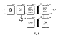
- Fig. 2 is a simplified block diagram that illustrates the most significant part of an inductive charger arrangement according to an embodiment of the invention.
- An AC supply voltage is brought into the input of a filtering and rectifying block 201 the task of which is to rectify the AC voltage and to prevent electromagnetic interference from entering from the AC mains supply to the inductive charger arrangement and equally to prevent electromagnetic interference generated within the inductive charger arrangement from propagating into the AC mains supply.
- the output of the filtering and rectifying block 201 is coupled to the input of a controllable pre-regulator 202 the task of which is to controllably convert the rectified supply voltage to another voltage.
- Said other voltage is led into a self-oscillating switching stage 203 the input of which is coupled to the output of the controllable pre-regulator 202.
- the output of the self-oscillating switching stage 203 is in turn coupled to the primary winding of a power transformer 204.
- a secondary winding of the power transformer 204 is coupled to a rectifying, filtering and regulating block 205 the task of which is to cyclically discharge energy from the magnetic field of the power transformer 204 and to convert it into a DC output voltage.
- a PWM controller 206 From the rectifying, filtering and regulating block 205 there is a measurement coupling to a PWM controller 206; the measurement coupling conveys to the PWM controller 206 certain measured values that are related to the DC output voltage and/or output current of the rectifying, filtering and regulating block 205.
- a PWM output of the PWM controller 206 is coupled to a first winding of a feedback transformer 207.
- a second winding of the feedback transformer 207 is coupled to the input of a filter 208.
- the filter 208 has a certain frequency response, which will be described in more detail later. From the output of the filter 208 there is a coupling through an amplifier 209 to a control input of the controllable pre-regulator 202.
- transformers 204 and 207 need not be conventional transformers in the sense that the primary and secondary windings would have a well-defined constant physical relation (for example so that in each transformer the primary and secondary windings would be wound around a common core).
- the windings of the transformers are located in mechanically separate entities so that the distance between a primary and a secondary winding as well as the relative directions of the windings depend heavily on the mechanical tolerances that are used in manufacturing said entities.
- the inductive charger arrangement that is schematically illustrated in fig. 2 operates as follows.
- the filtered and rectified output voltage of block 201 is brought as the input supply voltage to the controllable pre-regulator 202.
- the output voltage of the controllable pre-regulator 202 varies as a function of the duty cycle of a pulsed control signal that is brought into its control input.
- the self-oscillating switching stage 203 receives this variable output voltage of the controllable pre-regulator 202 as an input voltage that it uses as a source of the energy that it pumps cyclically to the magnetic field of the power transformer 204.
- the switching frequency or duty cycle of the self-oscillating switching stage 203 are not controlled by anything else than the selection of the component values that are used in its implementation.
- Such a self-oscillating switching stage is also referred to as (the primary part of) a resonant switched-mode power supply, because under steady-state conditions the switching frequency and duty cycle acquire certain essentially constant values that are determined by the resonance characteristics of the circuit.
- the output voltage of the controllable pre-regulator 202 was in turn a function of the duty cycle of a pulsed control signal that is brought into its control input, we may say that as a whole the controllable pre-regulator 202 and the self-oscillating switching stage 203 constitute the primary side of a PWM-controlled switched-mode power supply where the frequency of the PWM control pulses is not necessarily the same as the switching frequency at which power is pumped into the magnetic field of the power transformer 204. Below we will show that it is essential to the invention that these frequencies are different.
- the rectifying, filtering and regulating block 205 cyclically discharges energy from the magnetic field of the power transformer 204 at a frequency that is equal to that at which energy is pumped thereto by the primary side.
- the measurement performed by or for the PWM controller 206 may concern directly the DC output voltage and/or output current of the rectifying, filtering and regulating block 205, but this is not essential: a measurement of a quantity the value of which has a certain unambiguous relation to said DC output voltage and/or output current would do as well, as long as the PWM controller 206 has been programmed so that it interprets such unambiguous relation correctly.
- the PWM controller 206 varies the duty cycle of its output pulses so that the measured quantity would show that the DC output voltage and/or output current follows said voltage/current characteristics as closely as possible.
- the PWM controller 206 tries to keep the DC output voltage at a certain predefined level: if the measurement shows that the DC output voltage is below said level the duty cycle is increased, and correspondingly if the measurement shows that the DC output voltage is above said level the duty cycle is decreased.
- the frequency at which the PWM controller 206 gives its PWM output pulses is typically also a programmable value. According to the invention this frequency is selected so that it is different than the resonant switching frequency of the self-oscillating switching stage 203. Below we will give a detailed analysis on how far from each other the frequencies should most advantageously be.
- the PWM output pulses are transferred over the feedback transformer 207 back to the primary side.
- the frequency response of the filter 208 has been selected so that it defines a first range of frequencies to be passed and a second range of frequencies to be blocked. According to the invention the frequency at which the PWM controller 206 gives its PWM output pulses must be within the first range and the resonant switching frequency of the self-oscillating switching stage 203 must be within the second range.
- the PWM pulses which at this part of the circuit may also be designated as the feedback pulses, pass through the filter 208 while any spurious signals that result from electromagnetic coupling between the transformers 204 and 207, which occurs mainly at the switching frequency of the self-oscillating switching stage 203, are strongly attenuated.
- the "decontaminated" PWM pulses After filtering the "decontaminated" PWM pulses are amplified in the amplifier arrangement 209 and provided to the control input of the controllable pre-regulator 202.
- the distance in frequency units at which the frequency of the PWM output pulses from the PWM controller 206 must be from the resonant switching frequency of the self-oscillating switching stage 203, as well as the relative magnitudes of the frequencies, are affected by several factors. We may first discuss the latter issue. It is a known fact that the use of PWM control in a switched-mode power supply tends to set, at least at the priority date of this patent application, an upper limit to the usable range of switching frequencies. Usability in this sense means that the generation and handling of PWM pulses at the required accuracy becomes difficult, and remarkable switching losses are unavoidable, if the switching frequency becomes very high.
- the invention does not literally require that the relative magnitudes of the frequencies are selected in this way: at least theoretically it is possible to make the resonant switching frequency of the self-oscillating switching stage 203 lower than the frequency of the PWM output pulses from the PWM controller 206.
- the mechanical features of the portable electronic device and the charger determine, how close the transformer windings come within each transformer alone as well as to each other between transformers.
- the resonant switching frequency of the self-oscillating switching stage 203 is about 25 times the frequency of the PWM output pulses from the PWM controller 206 and the air gap per leg in an U-cored power transformer 204 (i.e. the distance between the core halves) is 2.6 mm.
- the inductances of the windings of the feedback transformer were 4.7 mH on the side of the PWM controller 206 and 1 mH on the side of the filter 208. It is possible to experiment with the values of the above-mentioned quantities in order to find other working combinations. Later improvements in the low pass filter combined with a simple technique of doubling the frequency of the feedback pulses, which will be described later in more detail, suggest that the resonant switching frequency of the self-oscillating switching stage need not be more than 6 times the frequency of the feedback pulses to achieve completely satisfactory results.
- each half of the power transformer had an U-core.
- the primary core had a 9 mm external width between the U legs, a total length of 5 mm for each leg from the bottom of the core, and a thickness of 3 mm.
- the dimensions of the secondary core were otherwise the same but the total length of the legs was slightly smaller.
- the primary and secondary windings both consisted of two separate windings, each being wound around a U leg of its own as close to the open end of the leg as possible.
- the U cores were placed so that the open ends of the U legs faced each other at a distance of 2.6 mm.
- Each winding of the feedback transformer was wound as a cylindrical coil around a ferrite rod having a thickness of approximately 0.8 mm.
- the ferrite rods were placed parallel to each other at an orthogonal axial displacement and a variable axial distance in the range of 3 to 12 mm.
- the direction of the ferrite rods was parallel to the direction of the bottom parts of the U cores in the power transformer, which means that the feedback windings were placed orthogonally against the direction of the power transformer coils.
- transformers for example one might consider placing cylindrical feedback coils on the same straight line so that their central axes would coincide, or one might use E cores for the power transformer so that the actual power transformer coils would be wound around the peripheral legs and the feedback coils would be wound around the center legs of the cores, with the open ends of the legs of the E cores facing each other in the transformer arrangement.
- the PWM pulse train that is to be transferred over the feedback transformer does not comprise, at least not intentionally, a DC component.
- the filter 208 does not need to be of a low-pass type. It may well be of a band-pass type with a relatively wide pass band. The requirement for the width of the pass band comes from the fact that basically we want to transfer essentially rectangular pulses, which means that it is not enough to pass the fundamental PWM frequency but a number of its harmonics must be passed as well. It may be even advantageous to use a band-pass filter instead of a low-pass one especially if we want to intentionally reject any spurious DC components.
- the component that implements the short-distance wireless feedback connection as a transformer.
- this is not a limitation: other kinds of short-distance wireless links such as capacitive transfer, an infrared transmitter-receiver pair or an optocoupler could be used as well.
- Some of these alternative embodiments gain remarkable advantage from the use of a band-pass filter instead of a low-pass one, because for example an infrared link is vulnerable to external low-frequency interference from the sun, artificial lighting and other known error sources.
- FIG. 3 illustrates the primary side of an inductive charger arrangement according to an embodiment of the invention.
- functional blocks that correspond to blocks 201, 202, 203, 208 and 209 of fig. 2 are shown in addition to said advantageous auxiliary features.
- the left-hand sides of the transformers designated as 204 and 207 in fig. 2 are represented in fig. 3.
- fig. 3 illustrates those parts that are located in the charger.
- a supply voltage generating block 301 takes 80...264 V AC or 10.8...28 V DC as an input voltage. For the purposes of simplifying the following description we may assume so far that the AC input voltage range is used.
- An output of the supply voltage generating block 301 is coupled to the input of a very low frequency clock 302; the frequency of 1 Hz is given in fig. 3 as an example.
- An output of the very low frequency clock 302 is coupled to the series coupling of a Schmitt trigger 303, a start oscillator 304 with an exemplary oscillating frequency of 47 kHz, a diode 305, a driver and latch block 306 and a pre-regulator 307, of which the latter is in fig.
- An output of the pre-regulator is coupled to the supply voltage input of a resonant switched-mode power supply 308 the outputs of which are in turn coupled to two windings 309 and 310 on an U-shaped core 311 of a power transformer.
- a reversely biased diode 315 couples the auxiliary supply voltage rail 314 to the pre-regulator 307.
- the Schmitt trigger block 303, the start oscillator block 304 and the driver and latch block 306 are all coupled to the auxiliary supply voltage rail 314. Further there is a high-voltage supply rail 316 that links the supply voltage generating block 301 essentially directly with the pre-regulator 307.
- the pickup winding 320 of a feedback transformer is coupled to a filter 321.
- the output of the filter 321 is coupled, through an AC amplifier 322, to a thresholding block 323.
- the output of the thresholding block 323 is coupled to the signal input of a DC amplifier 324.
- From the output of the DC amplifier 324 there are several signal paths, one of which goes through a front edge delay block 325, an additional amplifier 326 and a diode 327 to a point between diode 305 and the driver and latch block 306.
- Another signal path from the output of the DC amplifier 324 goes through a differentiation stage 328 and a diode 329 to a control input called the OFF input of the driver and latch block 306.
- the latter converts the supply voltage into a variable input voltage for the resonant switched-mode power supply 308, which in turn chops said variable input voltage in order to cyclically pump, through the primary windings 309 and 310, energy into the magnetic field of the power transformer.
- the resonance frequency of the resonant switched-mode power supply 308 is typically in the order of MHz; in the research work that led to the present invention a value of approximately 1.2 MHz was used, with values from 1.16 MHz to 1.6 MHz tested to show little practical significance to the key issues of the invention.
- pulse width modulated feedback pulses keep coming from the secondary side that is not shown in fig. 3. These are picked up by the pickup winding 320 and coupled to the filter 321.
- the pulse frequency of the feedback pulses was initially 47 kHz, but successful experiments were performed with feedback pulse frequencies of up to 200 kHz.
- the task of the filter 321 is to remove from the signal coming from the pickup winding 320 all high-frequency interference resulting from the power transformer, however so that the rectangular form of the feedback pulses is at least approximately preserved.
- the filter 321 may be a low-pass filter having only said upper cut-off frequency, or a band-pass filter in which case the lower cut-off frequency (the lower limit of the pass band) must lie below the pulse frequency of the feedback pulses.
- the filtered output of the filter 321 is amplified in the AC amplifier 322, which has most advantageously an automatic gain control amplification factor; this is illustrated schematically as the AGC block 332.
- the amplified pulses are taken to the thresholding block 323 the task of which is to reject residual ripple: a voltage swing from a level that is well below a threshold level to another level that is well above said threshold level is interpreted as the beginning of a pulse, whereas a corresponding voltage swing in the other direction is interpreted as the end of a pulse.
- the pulse width modulated feedback pulses should therefore appear essentially in the same form as the one they had at the output of the PWM controller on the secondary side (not shown in fig. 3).
- the leading and trailing edges of the feedback pulses are handled separately.
- the pulses as such are coupled both to the front edge delay block 325 and to the differentiation stage 328, but the couplings from the front edge delay block 325 through the amplifier 326 and diode 327 to the "ON" input of the driver and latch block 306 on one hand and from the differentiation stage 328 through the diode 329 to the "OFF" input of the driver and latch block 306 on the other hand are arranged so that only the leading (rising) edges of the pulses have an effect that is conveyed through the first-mentioned route and the trailing (falling) edges of the pulses have an effect that is conveyed through the last-mentioned route.
- the leading edges are slightly delayed in the front edge delay block 325.
- the reason thereto is the fact that the PWM controller that was used in the experimental coupling produces pulses at least at a minimum duty cycle of about 0,05. This is related to the upper bandpass limiting frequency of the filter 321; it is not possible to transfer needle pulses.
- the pre-regulator needs a wide range of PWM signals with duty cycles from practically zero to a certain maximum value. In the experimental coupling it was meant that the duty cycle could go all the way to zero (no pulses at all) if needed, and this was accomplished by delaying the leading edge of each pulse by an amount that was equal to the original minimum length of the pulses.
- the pre-regulator 307 which itself acts as a switched-mode power supply, receives pulse width modulated switching pulses at a frequency that is either the same as or two times that of the feedback pulses picked up by the pickup winding 320 and at a duty cycle that is slightly lower than that of the feedback pulses. Doubling the feedback pulse frequency is possible simply by inverting the negative part of the AC-type feedback pulse signal, which is symmetrical with respect to ground.
- This fact has to be taken into account in dimensioning the pre-regulator 307 and the resonant switched-mode power supply 308: it is simple as such to define the component values and other dimensioning factors so that each given duty cycle at the feedback transformer is mapped into a corresponding rate of transferring energy over the power transformer.
- the above-mentioned simple feedback pulse frequency doubling scheme in turn means that again the pre-regulator 307 and the resonant switched-mode power supply 308 must be dimensioned accordingly.
- pre-regulator 307 must start pre-regulating and the resonant switched-mode power supply 308 must start resonating already when no sufficient feedback is coming through the feedback transformer, and suitable soft-starting must be employed in order to avoid unnecessary and potentially harmful surges of energy at the starting moment.
- a non-charging state means that no feedback pulses are received, i.e. the blocks 320-329 at the lower part of fig. 3 are not operative in giving the driver and latch block 306 either ON or OFF commands.
- the pre-regulator 307 is generally not producing an output voltage at all; neither is it drawing energy from the high-voltage supply rail 316.
- the very low frequency clock 302 is operative and sets the switch 312 into an ON state regularly; for example for a period of 10 ms once every second. During these ON periods an auxiliary supply voltage is available at the auxiliary supply voltage rail 314 for the blocks coupled thereto, and so during said ON periods the start oscillator 304 produces switching pulses to the driver and latch block 306.
- Every such ON period represents an attempt of going into the charging state: for a short period of time the driver and latch block 306 gives - commanded by the start oscillator 304 - switching pulses to the pre-regulator 307, which in turn provides a certain amount of energy to the resonant switched-mode power supply 308 which pumps a kind of probing burst of energy into the magnetic field of the power transformer.
- the driver and latch block 306 gives - commanded by the start oscillator 304 - switching pulses to the pre-regulator 307, which in turn provides a certain amount of energy to the resonant switched-mode power supply 308 which pumps a kind of probing burst of energy into the magnetic field of the power transformer.
- the probing bursts start delivering energy to the feedback circuit of the device (not shown in fig. 3).
- the PWM controller contained therein (not shown in fig. 3) gradually starts to produce feedback pulses that are coupled to the pickup winding 320.
- the feedback pulses that come through the blocks 320-329 must replace the pulses coming from the start oscillator 304 as the ones that control the operation of the driver and latch block 306.
- One possibility for implementing the detection of an "illegal object" condition is to select a threshold level at a second thresholding block that is driven by a second AC-amplifier without automatic gain control so that attenuated feedback pulses would not suffice to be detected. Said possibility also calls for adding a peak-to-peak detector between the output of such a second AC amplifier and such a second thresholding block. Note that the amplification factor of the AC amplifier 322 involves automatic gain control, so attenuated feedback pulses would not result in attenuated output pulses from the AC amplifier 322. An output from said peak to peak detector could then be used for example to either enable or disable the passing of the feedback pulses further, depending on whether the peak to peak value of the AC amplified feedback signal was found to be sufficient or not.
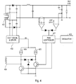
- Fig. 4 is an exemplary block diagram of the secondary side, which in our exemplary embodiment is located within the device the battery of which is to be charged. Not all parts of the secondary side need to be discussed in detail.
- a secondary power winding 401 that, together with its associated rectifying and filtering circuitry, cyclically discharges energy from the magnetic field of the power transformer. This energy is used, in addition to generating the secondary voltage that is the output voltage of the whole arrangement, in a voltage doubler and stabile auxiliary voltage generator 402 to generate a voltage which is used as the energy source for the pulses that are to be fed into the feedback transformer.
- a switching source for these pulses there is the PWM controller 407, the operating frequency of which comes from an associated oscillator 403.
- the switching pulses themselves do not contain sufficient power to be fed into the feedback transformer, so two constant current sources 404 and 405 that are coupled to the output of the voltage doubler and stabile auxiliary voltage generator 402 are used in series with their associated switching transistors.
- the bases of the switching transistors receive the switching pulses from the PWM controller 407 at a mutual phase shift of 180 degrees.
- the signal over the transmitting winding 406 is the difference signal of the phase shifted and pulse width modulated output signals of the PWM controller 407.
- the couplings to the ends of the transmitting winding 406 of the feedback transformer are from the collectors of the switching transistors.
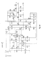
- Figs. 5a to 5d illustrate a detailed circuit diagram of the primary side, i.e. the charger side, of a charger that follows the structural principle of fig. 3.
- the circuit diagram is not exactly the optimal solution regarding the detection of an insufficient amplitude of the feedback pulses.
- Increasing the feedback pulse frequency towards 200 kHz and/or decreasing the resonance frequency of the resonant switched-mode power supply towards 1 MHz means that certain changes must be made in the circuit diagram of figs. 5a to 5d.
- the resonance capacitors that relate to the resonance frequency of the resonant switched-mode power supply on both the primary and the secondary side must be increased in capacitance in order to decrease the frequency.
- the component values that set the pulse frequency of the feedback pulse generator on the secondary side must be selected appropriately. Such dimensioning of circuits belongs to routine workshop modifications of a disclosed principle, and are well within the capability of a person skilled in the art.
- the circuit built around transistor T31 for detection of the "illegal object” condition should activate a shutdown circuit only after a sufficient delay which is large in comparison with the time factors involved in the starting procedure but still relatively small compared with the time it takes to cause significant overheating when the "illegal object” condition occurs.
- the efficiency of an inductively coupled switched-mode power supply is intimately coupled to the coupling coefficient of the power transformer.
- a simple way to increase the value of the coupling coefficient is to bring the halves of the power transformer closer to each other.
- the devices could be mechanically designed so that they include the halves of the power transformer very close to their outer surface, so that when the portable electronic device is placed into the receptive socket, the physical separation of the transformer halves is as small as possible.
Landscapes
- Engineering & Computer Science (AREA)
- Power Engineering (AREA)
- Computer Networks & Wireless Communication (AREA)
- Dc-Dc Converters (AREA)
- Charge And Discharge Circuits For Batteries Or The Like (AREA)
Applications Claiming Priority (2)
| Application Number | Priority Date | Filing Date | Title |
|---|---|---|---|
| FI20002493A FI20002493A7 (fi) | 2000-11-14 | 2000-11-14 | Teholähdejärjestely ja induktiivisesti kytketty akkulaturi, jossa on langattomasti kytketty ohjaus, ja menetelmä teholähdejärjestelyn ja induktiivisesti kytketyn akkulaturin ohjaamiseksi langattomasti |
| FI20002493 | 2000-11-14 |
Publications (1)
| Publication Number | Publication Date |
|---|---|
| EP1209791A2 true EP1209791A2 (de) | 2002-05-29 |
Family
ID=8559492
Family Applications (1)
| Application Number | Title | Priority Date | Filing Date |
|---|---|---|---|
| EP01660205A Withdrawn EP1209791A2 (de) | 2000-11-14 | 2001-11-14 | Stromversorgungsschaltung und induktiv gekoppeltes Batterieladegerät mit drahtlos gekoppelter Steuerung und dazu gehörendes Verfahren |
Country Status (4)
| Country | Link |
|---|---|
| US (1) | US20020057584A1 (de) |
| EP (1) | EP1209791A2 (de) |
| JP (1) | JP2002199712A (de) |
| FI (1) | FI20002493A7 (de) |
Cited By (18)
| Publication number | Priority date | Publication date | Assignee | Title |
|---|---|---|---|---|
| WO2003098773A1 (en) * | 2002-05-16 | 2003-11-27 | Koninklijke Philips Electronics N.V. | Single stage power converter for contact-less energy transfer |
| WO2004073150A1 (en) | 2003-02-04 | 2004-08-26 | Access Business Group International Llc | Adaptive inductive power supply |
| WO2004040857A3 (de) * | 2002-10-28 | 2004-08-26 | Siemens Ag | Verfahren zur datenübertragung von daten zur positionsbestimmung mit bluetooth-technologie |
| WO2004073176A3 (en) * | 2003-02-04 | 2005-03-17 | Access Business Group Int Llc | Adapter |
| US7180248B2 (en) | 1999-06-21 | 2007-02-20 | Access Business Group International, Llc | Inductively coupled ballast circuit |
| US7385357B2 (en) | 1999-06-21 | 2008-06-10 | Access Business Group International Llc | Inductively coupled ballast circuit |
| US7408324B2 (en) | 2004-10-27 | 2008-08-05 | Access Business Group International Llc | Implement rack and system for energizing implements |
| US7462951B1 (en) | 2004-08-11 | 2008-12-09 | Access Business Group International Llc | Portable inductive power station |
| WO2009089253A1 (en) * | 2008-01-07 | 2009-07-16 | Access Business Group International Llc | Inductive power supply with duty cycle control |
| WO2009090235A3 (de) * | 2008-01-18 | 2009-09-17 | Giesecke & Devrient Gmbh | Vorrichtung zum ansteuern eines aktuators |
| EP1787382A4 (de) * | 2004-08-20 | 2009-12-02 | Analog Devices Inc | Leistungs- und informationssignaltransfer unter verwendung von mikrotransformatoren |
| US8054651B2 (en) | 2006-08-09 | 2011-11-08 | Mbda Uk Limited | Simple and effective self regulating inductive power transfer system |
| CN103107709A (zh) * | 2003-02-04 | 2013-05-15 | 通达商业集团国际公司 | 具有通信能力的自适应感应电源 |
| US9293997B2 (en) | 2013-03-14 | 2016-03-22 | Analog Devices Global | Isolated error amplifier for isolated power supplies |
| US9660848B2 (en) | 2014-09-15 | 2017-05-23 | Analog Devices Global | Methods and structures to generate on/off keyed carrier signals for signal isolators |
| US9998301B2 (en) | 2014-11-03 | 2018-06-12 | Analog Devices, Inc. | Signal isolator system with protection for common mode transients |
| US10270630B2 (en) | 2014-09-15 | 2019-04-23 | Analog Devices, Inc. | Demodulation of on-off-key modulated signals in signal isolator systems |
| US10536309B2 (en) | 2014-09-15 | 2020-01-14 | Analog Devices, Inc. | Demodulation of on-off-key modulated signals in signal isolator systems |
Families Citing this family (61)
| Publication number | Priority date | Publication date | Assignee | Title |
|---|---|---|---|---|
| GB0229141D0 (en) | 2002-12-16 | 2003-01-15 | Splashpower Ltd | Improvements relating to contact-less power transfer |
| US6936975B2 (en) * | 2003-04-15 | 2005-08-30 | 02Micro International Limited | Power supply for an LCD panel |
| NO320439B1 (no) * | 2004-04-30 | 2005-12-05 | Geir Olav Gyland | Anordning og fremgangsmate for kontaktlos energioverforing |
| US7126289B2 (en) * | 2004-08-20 | 2006-10-24 | O2 Micro Inc | Protection for external electrode fluorescent lamp system |
| US9130602B2 (en) * | 2006-01-18 | 2015-09-08 | Qualcomm Incorporated | Method and apparatus for delivering energy to an electrical or electronic device via a wireless link |
| US8447234B2 (en) | 2006-01-18 | 2013-05-21 | Qualcomm Incorporated | Method and system for powering an electronic device via a wireless link |
| MX2009008011A (es) * | 2007-01-29 | 2010-02-18 | Powermat Ltd | Acoplamiento de energia sin clavija y metodo para controlar la transferenca de la energia atraves de un acoplamiento inductivo. |
| KR100999770B1 (ko) | 2007-02-20 | 2010-12-08 | 세이코 엡슨 가부시키가이샤 | 송전 제어 장치, 송전 장치, 전자 기기 및 무접점 전력전송 시스템 |
| US9774086B2 (en) * | 2007-03-02 | 2017-09-26 | Qualcomm Incorporated | Wireless power apparatus and methods |
| CN102106054A (zh) | 2007-03-22 | 2011-06-22 | 鲍尔马特有限公司 | 信号传递系统 |
| US7602142B2 (en) * | 2007-04-02 | 2009-10-13 | Visteon Global Technologies, Inc. | System for inductive power transfer |
| US9124120B2 (en) | 2007-06-11 | 2015-09-01 | Qualcomm Incorporated | Wireless power system and proximity effects |
| US7804197B2 (en) * | 2007-06-29 | 2010-09-28 | Seiko Epson Corporation | Power transmission control device, power transmission device, electronic instrument, and non-contact power transmission system |
| CN101842962B (zh) * | 2007-08-09 | 2014-10-08 | 高通股份有限公司 | 增加谐振器的q因数 |
| EP2188863A1 (de) | 2007-09-13 | 2010-05-26 | QUALCOMM Incorporated | Maximierung des pulverertrags aus drahtlosen leistungsmagnetresonatoren |
| EP2201641A1 (de) * | 2007-09-17 | 2010-06-30 | Qualcomm Incorporated | Sender und empfänger für drahtlosen energietransfer |
| AU2008303118A1 (en) * | 2007-09-25 | 2009-04-02 | Powermat Technologies Ltd. | Inductive power transmission platform |
| US10068701B2 (en) | 2007-09-25 | 2018-09-04 | Powermat Technologies Ltd. | Adjustable inductive power transmission platform |
| EP2208279A4 (de) * | 2007-10-11 | 2016-11-30 | Qualcomm Inc | Drahtloser stromtransfer unter verwendung von magnetomechanischen systemen |
| US8193769B2 (en) * | 2007-10-18 | 2012-06-05 | Powermat Technologies, Ltd | Inductively chargeable audio devices |
| US20100219183A1 (en) * | 2007-11-19 | 2010-09-02 | Powermat Ltd. | System for inductive power provision within a bounding surface |
| US8536737B2 (en) * | 2007-11-19 | 2013-09-17 | Powermat Technologies, Ltd. | System for inductive power provision in wet environments |
| RU2010133056A (ru) * | 2008-01-07 | 2012-02-20 | Эксесс Бизнес Груп Интернейшнл Ллс (Us) | Беспроводной силовой адаптер для компьютера |
| US9960640B2 (en) | 2008-03-17 | 2018-05-01 | Powermat Technologies Ltd. | System and method for regulating inductive power transmission |
| US9331750B2 (en) | 2008-03-17 | 2016-05-03 | Powermat Technologies Ltd. | Wireless power receiver and host control interface thereof |
| US7956491B2 (en) * | 2008-03-17 | 2011-06-07 | Asic Advantage Inc. | Integrated multi-transformer |
| KR20100130215A (ko) * | 2008-03-17 | 2010-12-10 | 파우워매트 엘티디. | 유도송전장치 |
| US9960642B2 (en) | 2008-03-17 | 2018-05-01 | Powermat Technologies Ltd. | Embedded interface for wireless power transfer to electrical devices |
| US9337902B2 (en) | 2008-03-17 | 2016-05-10 | Powermat Technologies Ltd. | System and method for providing wireless power transfer functionality to an electrical device |
| US8629576B2 (en) * | 2008-03-28 | 2014-01-14 | Qualcomm Incorporated | Tuning and gain control in electro-magnetic power systems |
| US8320143B2 (en) * | 2008-04-15 | 2012-11-27 | Powermat Technologies, Ltd. | Bridge synchronous rectifier |
| US20090299918A1 (en) * | 2008-05-28 | 2009-12-03 | Nigelpower, Llc | Wireless delivery of power to a mobile powered device |
| CA2726552A1 (en) * | 2008-06-02 | 2009-12-10 | Powermat Ltd. | Appliance mounted power outlets |
| US8981598B2 (en) | 2008-07-02 | 2015-03-17 | Powermat Technologies Ltd. | Energy efficient inductive power transmission system and method |
| US8188619B2 (en) | 2008-07-02 | 2012-05-29 | Powermat Technologies Ltd | Non resonant inductive power transmission system and method |
| US11979201B2 (en) | 2008-07-02 | 2024-05-07 | Powermat Technologies Ltd. | System and method for coded communication signals regulating inductive power transmissions |
| WO2010005324A1 (en) * | 2008-07-07 | 2010-01-14 | Powerbyproxi Limited | A contactless power receiver and method of operation |
| AU2009269574A1 (en) * | 2008-07-08 | 2010-01-14 | Powermat Technologies Ltd. | Display device |
| AU2009297963A1 (en) * | 2008-09-23 | 2010-04-01 | Powermat Technologies Ltd. | Combined antenna and inductive power receiver |
| JP5554937B2 (ja) * | 2009-04-22 | 2014-07-23 | パナソニック株式会社 | 非接触給電システム |
| US7990070B2 (en) * | 2009-06-05 | 2011-08-02 | Louis Robert Nerone | LED power source and DC-DC converter |
| US20100321968A1 (en) * | 2009-06-18 | 2010-12-23 | Hamilton Sundstrand Corporation | Load fault handling for switched reluctance or induction type machines |
| IT1400748B1 (it) * | 2010-06-30 | 2013-07-02 | St Microelectronics Srl | Apparato per il trasferimento wireless di energia fra due dispositivi e contemporaneo trasferimento di dati. |
| NZ589312A (en) | 2010-11-16 | 2013-03-28 | Powerbyproxi Ltd | Battery having inductive power pickup coils disposed within the battery casing and at an angle to the casing axis |
| KR101373769B1 (ko) * | 2011-02-15 | 2014-03-14 | 성균관대학교산학협력단 | 고효율 가변전력 전송 장치 및 방법 |
| JP5289489B2 (ja) * | 2011-03-17 | 2013-09-11 | 三菱電機株式会社 | 車両充電装置 |
| US8907580B2 (en) * | 2013-02-02 | 2014-12-09 | Supertex, Inc. | Circuit and method for flicker suppression in light emitting diodes (LEDs) |
| WO2014132345A1 (ja) * | 2013-02-27 | 2014-09-04 | 日立オートモティブシステムズ株式会社 | 電源起動システム |
| US9774208B2 (en) | 2013-06-10 | 2017-09-26 | Cellco Partnership | NFC assisted wireless charging |
| US9973038B2 (en) * | 2013-06-10 | 2018-05-15 | Celico Partnership | Self optimizing antenna for NFC and wireless charging |
| US9601267B2 (en) | 2013-07-03 | 2017-03-21 | Qualcomm Incorporated | Wireless power transmitter with a plurality of magnetic oscillators |
| US9211799B2 (en) * | 2013-08-15 | 2015-12-15 | Telefonix, Inc. | Mechanism for locking and fault detection in the electrical vehicle supply equipment cord |
| US9362755B2 (en) | 2013-12-16 | 2016-06-07 | Texas Instruments Incorporated | Circuit and architecture for a demodulator for a wireless power transfer system and method therefor |
| KR20160030672A (ko) * | 2014-09-11 | 2016-03-21 | 삼성전기주식회사 | 무선 전력 수신 장치 및 무선 전력 송수신 시스템 |
| US9838084B2 (en) | 2014-09-30 | 2017-12-05 | Texas Instruments Incorporated | Control of a tank circuit in a wireless power transmission system providing FSK communication |
| CN104578819B (zh) * | 2014-12-19 | 2017-05-10 | 中国石油天然气集团公司 | 水下勘探中频甲板电源及电磁勘探系统 |
| CN106487103B (zh) * | 2015-08-11 | 2019-03-05 | 纽艾吉科技有限公司 | 无线充电系统及其无线送电装置与无线送电方法 |
| EP3512087B1 (de) | 2018-01-12 | 2023-01-25 | STMicroelectronics S.r.l. | Galvanisch isolierte gleichspannungswandlerschaltung mit datenkommunikation, entsprechendes system und entsprechendes verfahren |
| IT201800004174A1 (it) * | 2018-04-03 | 2019-10-03 | Circuito e sistema ad isolamento galvanico, procedimento corrispondente | |
| TWI645648B (zh) * | 2018-04-03 | 2018-12-21 | 群光電能科技股份有限公司 | 充電裝置與應用於充電裝置之適應性分頻控制方法 |
| CN112393795B (zh) * | 2020-11-25 | 2022-03-15 | 深圳市西城微科电子有限公司 | 一种电子秤的数字处理方法及电子秤 |
-
2000
- 2000-11-14 FI FI20002493A patent/FI20002493A7/fi not_active IP Right Cessation
-
2001
- 2001-11-13 JP JP2001347833A patent/JP2002199712A/ja active Pending
- 2001-11-13 US US10/011,537 patent/US20020057584A1/en not_active Abandoned
- 2001-11-14 EP EP01660205A patent/EP1209791A2/de not_active Withdrawn
Cited By (35)
| Publication number | Priority date | Publication date | Assignee | Title |
|---|---|---|---|---|
| US7180248B2 (en) | 1999-06-21 | 2007-02-20 | Access Business Group International, Llc | Inductively coupled ballast circuit |
| US7385357B2 (en) | 1999-06-21 | 2008-06-10 | Access Business Group International Llc | Inductively coupled ballast circuit |
| WO2003098773A1 (en) * | 2002-05-16 | 2003-11-27 | Koninklijke Philips Electronics N.V. | Single stage power converter for contact-less energy transfer |
| WO2004040857A3 (de) * | 2002-10-28 | 2004-08-26 | Siemens Ag | Verfahren zur datenübertragung von daten zur positionsbestimmung mit bluetooth-technologie |
| CN103107709A (zh) * | 2003-02-04 | 2013-05-15 | 通达商业集团国际公司 | 具有通信能力的自适应感应电源 |
| US9246356B2 (en) | 2003-02-04 | 2016-01-26 | Access Business Group International Llc | Adaptive inductive power supply |
| EP2405552A3 (de) * | 2003-02-04 | 2015-05-06 | Access Business Group International LLC | Adaptiv induktives Netzteil |
| EP2405564A3 (de) * | 2003-02-04 | 2015-04-29 | Access Business Group International LLC | Adaptiv induktives Netzteil |
| WO2004073150A1 (en) | 2003-02-04 | 2004-08-26 | Access Business Group International Llc | Adaptive inductive power supply |
| US10505385B2 (en) | 2003-02-04 | 2019-12-10 | Philips Ip Ventures B.V. | Adaptive inductive power supply |
| EP2403096A3 (de) * | 2003-02-04 | 2014-01-22 | Access Business Group International LLC | Einstellbare induktive Stromversorgung mit Kommunikation |
| EP2403095A3 (de) * | 2003-02-04 | 2014-01-22 | Access Business Group International LLC | Einstellbare induktive Stromversorgung mit Kommunikation |
| KR101047702B1 (ko) * | 2003-02-04 | 2011-07-08 | 액세스 비지니스 그룹 인터내셔날 엘엘씨 | 적응성 유도성 전원 |
| EP2242161A3 (de) * | 2003-02-04 | 2014-01-22 | Access Business Group International LLC | Einstellbare Induktionsstromversorgung in Kommunikationsanwendungen |
| US9906049B2 (en) | 2003-02-04 | 2018-02-27 | Access Business Group International Llc | Adaptive inductive power supply |
| US9190874B2 (en) | 2003-02-04 | 2015-11-17 | Access Business Group International Llc | Adaptive inductive power supply |
| CN103107709B (zh) * | 2003-02-04 | 2016-03-16 | 通达商业集团国际公司 | 具有通信能力的自适应感应电源 |
| WO2004073176A3 (en) * | 2003-02-04 | 2005-03-17 | Access Business Group Int Llc | Adapter |
| US7462951B1 (en) | 2004-08-11 | 2008-12-09 | Access Business Group International Llc | Portable inductive power station |
| US7706154B2 (en) | 2004-08-20 | 2010-04-27 | Analog Devices, Inc. | Power and information signal transfer using micro-transformers |
| EP1787382A4 (de) * | 2004-08-20 | 2009-12-02 | Analog Devices Inc | Leistungs- und informationssignaltransfer unter verwendung von mikrotransformatoren |
| US7408324B2 (en) | 2004-10-27 | 2008-08-05 | Access Business Group International Llc | Implement rack and system for energizing implements |
| US8054651B2 (en) | 2006-08-09 | 2011-11-08 | Mbda Uk Limited | Simple and effective self regulating inductive power transfer system |
| WO2009089253A1 (en) * | 2008-01-07 | 2009-07-16 | Access Business Group International Llc | Inductive power supply with duty cycle control |
| AU2009204283B2 (en) * | 2008-01-07 | 2013-08-22 | Access Business Group International Llc | Inductive power supply with duty cycle control |
| US9257851B2 (en) | 2008-01-07 | 2016-02-09 | Access Business Group International Llc | Inductive power supply with duty cycle control |
| US8129864B2 (en) | 2008-01-07 | 2012-03-06 | Access Business Group International Llc | Inductive power supply with duty cycle control |
| US10170935B2 (en) | 2008-01-07 | 2019-01-01 | Philips Ip Ventures B.V. | Inductive power supply with duty cycle control |
| US8482377B2 (en) | 2008-01-18 | 2013-07-09 | Giesecke & Devrient Gmbh | Device for controlling an actuator |
| WO2009090235A3 (de) * | 2008-01-18 | 2009-09-17 | Giesecke & Devrient Gmbh | Vorrichtung zum ansteuern eines aktuators |
| US9293997B2 (en) | 2013-03-14 | 2016-03-22 | Analog Devices Global | Isolated error amplifier for isolated power supplies |
| US9660848B2 (en) | 2014-09-15 | 2017-05-23 | Analog Devices Global | Methods and structures to generate on/off keyed carrier signals for signal isolators |
| US10270630B2 (en) | 2014-09-15 | 2019-04-23 | Analog Devices, Inc. | Demodulation of on-off-key modulated signals in signal isolator systems |
| US10536309B2 (en) | 2014-09-15 | 2020-01-14 | Analog Devices, Inc. | Demodulation of on-off-key modulated signals in signal isolator systems |
| US9998301B2 (en) | 2014-11-03 | 2018-06-12 | Analog Devices, Inc. | Signal isolator system with protection for common mode transients |
Also Published As
| Publication number | Publication date |
|---|---|
| JP2002199712A (ja) | 2002-07-12 |
| US20020057584A1 (en) | 2002-05-16 |
| FI20002493A0 (fi) | 2000-11-14 |
| FI20002493A7 (fi) | 2002-05-15 |
Similar Documents
| Publication | Publication Date | Title |
|---|---|---|
| EP1209791A2 (de) | Stromversorgungsschaltung und induktiv gekoppeltes Batterieladegerät mit drahtlos gekoppelter Steuerung und dazu gehörendes Verfahren | |
| CN104604082B (zh) | 用于无线地传送电力的设备和方法以及计算机可读介质 | |
| US10128688B2 (en) | Systems and methods for limiting voltage in wireless power receivers | |
| EP3022823B1 (de) | System und verfahren für gleichzeitige effiziente datenübertragung und drahtlose stromübertragung | |
| EP2745397B1 (de) | Überlastungserkennung und -prophylaxe für einen klasse-e-verstärker | |
| JP3692541B2 (ja) | 電力伝送装置及び電力伝送方法 | |
| CN110011433B (zh) | 用于使用闭合磁性回路的感应充电的系统及方法 | |
| US9368975B2 (en) | High power RF field effect transistor switching using DC biases | |
| JP3906708B2 (ja) | 非接触電力伝達装置 | |
| US20130077360A1 (en) | Systems, methods, and apparatus for rectifier filtering for input waveform shaping | |
| US9496755B2 (en) | Systems, methods, and apparatus for rectifier filtering for input waveform shaping | |
| CN104604093B (zh) | 用于电力发射器的保护装置及方法 | |
| CN107104515A (zh) | Ss‑l无线电力传输补偿电路 | |
| WO2013126342A2 (en) | Push-pull driver with stage inversion and method of operation | |
| JPWO2015053246A1 (ja) | ワイヤレス電力伝送システム | |
| Anwar et al. | A 6.78-MHz burst-mode controlled inductive wireless power transfer system for biomedical implants with back-channel communication eliminated using transmitter Q-factor detection | |
| US20230343504A1 (en) | Improved performance of converter | |
| US20210021156A1 (en) | True optimizable wireless power systems | |
| JP2003037950A (ja) | 非接触電力伝達装置 | |
| CN217486399U (zh) | 一种单管反激式直流稳压电路 | |
| CN120498144B (zh) | 一种无线充电系统的近场通讯方法 | |
| JPH08275402A (ja) | 電磁誘導コイル駆動回路 | |
| Jamal et al. | Simulation Study on Self-Frequency Tracking Control Strategy for Inductive Power Transfer System | |
| CN117748964A (zh) | 一种基于谐振环的高频双e类逆变器系统 | |
| JP3181263U (ja) | 非接触トランス |
Legal Events
| Date | Code | Title | Description |
|---|---|---|---|
| PUAI | Public reference made under article 153(3) epc to a published international application that has entered the european phase |
Free format text: ORIGINAL CODE: 0009012 |
|
| AK | Designated contracting states |
Kind code of ref document: A2 Designated state(s): AT BE CH CY DE DK ES FI FR GB GR IE IT LI LU MC NL PT SE TR |
|
| AX | Request for extension of the european patent |
Free format text: AL;LT;LV;MK;RO;SI |
|
| STAA | Information on the status of an ep patent application or granted ep patent |
Free format text: STATUS: THE APPLICATION IS DEEMED TO BE WITHDRAWN |
|
| 18D | Application deemed to be withdrawn |
Effective date: 20040531 |