EP1213826A2 - Schaltenlastungsnetzwerk für Leistungshalbleiterschalter - Google Patents
Schaltenlastungsnetzwerk für Leistungshalbleiterschalter Download PDFInfo
- Publication number
- EP1213826A2 EP1213826A2 EP01250433A EP01250433A EP1213826A2 EP 1213826 A2 EP1213826 A2 EP 1213826A2 EP 01250433 A EP01250433 A EP 01250433A EP 01250433 A EP01250433 A EP 01250433A EP 1213826 A2 EP1213826 A2 EP 1213826A2
- Authority
- EP
- European Patent Office
- Prior art keywords
- power semiconductor
- semiconductor switches
- relief
- diode
- series
- Prior art date
- Legal status (The legal status is an assumption and is not a legal conclusion. Google has not performed a legal analysis and makes no representation as to the accuracy of the status listed.)
- Withdrawn
Links
Images









Classifications
-
- H—ELECTRICITY
- H02—GENERATION; CONVERSION OR DISTRIBUTION OF ELECTRIC POWER
- H02M—APPARATUS FOR CONVERSION BETWEEN AC AND AC, BETWEEN AC AND DC, OR BETWEEN DC AND DC, AND FOR USE WITH MAINS OR SIMILAR POWER SUPPLY SYSTEMS; CONVERSION OF DC OR AC INPUT POWER INTO SURGE OUTPUT POWER; CONTROL OR REGULATION THEREOF
- H02M1/00—Details of apparatus for conversion
- H02M1/32—Means for protecting converters other than automatic disconnection
- H02M1/34—Snubber circuits
-
- H—ELECTRICITY
- H02—GENERATION; CONVERSION OR DISTRIBUTION OF ELECTRIC POWER
- H02M—APPARATUS FOR CONVERSION BETWEEN AC AND AC, BETWEEN AC AND DC, OR BETWEEN DC AND DC, AND FOR USE WITH MAINS OR SIMILAR POWER SUPPLY SYSTEMS; CONVERSION OF DC OR AC INPUT POWER INTO SURGE OUTPUT POWER; CONTROL OR REGULATION THEREOF
- H02M7/00—Conversion of AC power input into DC power output; Conversion of DC power input into AC power output
- H02M7/42—Conversion of DC power input into AC power output without possibility of reversal
- H02M7/44—Conversion of DC power input into AC power output without possibility of reversal by static converters
- H02M7/48—Conversion of DC power input into AC power output without possibility of reversal by static converters using discharge tubes with control electrode or semiconductor devices with control electrode
- H02M7/53—Conversion of DC power input into AC power output without possibility of reversal by static converters using discharge tubes with control electrode or semiconductor devices with control electrode using devices of a triode or transistor type requiring continuous application of a control signal
- H02M7/537—Conversion of DC power input into AC power output without possibility of reversal by static converters using discharge tubes with control electrode or semiconductor devices with control electrode using devices of a triode or transistor type requiring continuous application of a control signal using semiconductor devices only, e.g. single switched pulse inverters
- H02M7/5387—Conversion of DC power input into AC power output without possibility of reversal by static converters using discharge tubes with control electrode or semiconductor devices with control electrode using devices of a triode or transistor type requiring continuous application of a control signal using semiconductor devices only, e.g. single switched pulse inverters in a bridge configuration
-
- H—ELECTRICITY
- H02—GENERATION; CONVERSION OR DISTRIBUTION OF ELECTRIC POWER
- H02M—APPARATUS FOR CONVERSION BETWEEN AC AND AC, BETWEEN AC AND DC, OR BETWEEN DC AND DC, AND FOR USE WITH MAINS OR SIMILAR POWER SUPPLY SYSTEMS; CONVERSION OF DC OR AC INPUT POWER INTO SURGE OUTPUT POWER; CONTROL OR REGULATION THEREOF
- H02M1/00—Details of apparatus for conversion
- H02M1/32—Means for protecting converters other than automatic disconnection
- H02M1/34—Snubber circuits
- H02M1/342—Active non-dissipative snubbers
-
- Y—GENERAL TAGGING OF NEW TECHNOLOGICAL DEVELOPMENTS; GENERAL TAGGING OF CROSS-SECTIONAL TECHNOLOGIES SPANNING OVER SEVERAL SECTIONS OF THE IPC; TECHNICAL SUBJECTS COVERED BY FORMER USPC CROSS-REFERENCE ART COLLECTIONS [XRACs] AND DIGESTS
- Y02—TECHNOLOGIES OR APPLICATIONS FOR MITIGATION OR ADAPTATION AGAINST CLIMATE CHANGE
- Y02B—CLIMATE CHANGE MITIGATION TECHNOLOGIES RELATED TO BUILDINGS, e.g. HOUSING, HOUSE APPLIANCES OR RELATED END-USER APPLICATIONS
- Y02B70/00—Technologies for an efficient end-user side electric power management and consumption
- Y02B70/10—Technologies improving the efficiency by using switched-mode power supplies [SMPS], i.e. efficient power electronics conversion e.g. power factor correction or reduction of losses in power supplies or efficient standby modes
Definitions
- the present invention relates to the field of power electronics, in particular in the field of converter technology and particularly in switching relief networks for power semiconductor switches.
- IGBTs are also increasingly used as power semiconductor switches used in high-performance converters. IGBTs need in contrast to gate turn off thyristors or GTO thyristors in principle no switching relief network. Nevertheless, these are, at high switching frequencies and high switching power to reduce the switching power loss of the Semiconductor switch is preferably used.
- a method for switching relief of IGBTs is known.
- the associated switching relief network is shown in Fig. 15.
- a resonant wiring network consisting of the current limiting inductor L CL , the resonance capacitor C RES , the control semiconductor switch V RES with antiparallel diode is used D RES and the cut-off relief capacitor C CL, the control semiconductor switch V CL and the diode D CL connected antiparallel to it.
- the current to be switched off is reduced by a resonant oscillation process and the switching voltage is reduced to zero at the start of the switch-off process.
- the voltage rise rate occurring during the switch-off process is limited by the resonance capacitor C RES , the switch-off overvoltage by the resonance and switch-off relief capacitors acting in parallel.
- the control semiconductor V CL remains switched off at low current during the switch-off processes of the power semiconductor switches V 11 to V 16 .
- the diode D CL which is antiparallel to it, conducts the energy stored in the current limiting inductor L CL into the cut-off relief capacitor C CL , which is thus charged somewhat above the intermediate circuit voltage level.
- a resonant circuit current is built up, which reduces the current amplitude in the current limiting inductor L CL .
- the predeterminable value of the current up to which the control semiconductor V CL remains in the conductive state is specified as a function of a balanced energy balance of the switch-off relief capacitor C CL during a full switching cycle of the power semiconductor switches V 11 to V 16 ; half of the current flowing through the power semiconductor switch V 11 to V 16 to the load is preferably selected.
- the relevant power semiconductor switch V 11 to V 16 is controlled in the blocking state, as a result of which the load current, driven by the stored energy in the current limiting inductor L CL, is directed via the diode D CL into the cut-off relief capacitor C CL and, in addition, the control semiconductor switch V CL commutated with almost no loss.
- DE 197 30 038 C1 discloses a circuit variant according to FIG. 17 that is theoretically theoretical and shows an arrangement for returning the wiring energy in a bridge circuit.
- the current limiting inductor L CL is also arranged in series and the cut-off relief capacitor C CL is also arranged in parallel with the power semiconductor switches V 11 to V 16 .
- the cut-off relief capacitor C CL is also partially decoupled from the intermediate circuit via a diode D CL polarized in the direction of the cut-off relief capacitor C CL .
- this circuit corresponds to the approach according to DE 196 36 248 C1 (Fig.
- FIG. 1 shows a switch-on relief network for power semiconductor switches with a resonant circuit converter arranged in series with the switch-off relief capacitor C CL , for feeding back the excess energy of the switch-off relief capacitor C CL .
- the resonant circuit converter is controlled independently of the power semiconductor switches V 11 to V 16 of the main converter.
- the power semiconductor switches V 11 to V 16 together with their anti-parallel reworking diodes D 11 to D 16 are part of a bridge circuit between a first pole of a DC voltage source, the connection of a load, which is shown in FIG. 1 is not shown and interconnects a second pole of the DC voltage source.
- a current limiting choke coil L CL is formed in the feed line of the first pole of the DC voltage source to the bridge circuit.
- the current limiting choke coil can optionally also be divided into two current limiting choke coils, the second current limiting choke coil being arranged in the supply line to the second pole of the DC voltage source for the bridge circuit, between the connections of the resonance capacitor C RES (description see below) and the cut-off relief capacitor C CL .
- a resonant circuit converter is designed in series with the cut-off relief capacitor C CL .
- This resonant circuit converter comprises two series-connected semiconductor switches V res1 , V res2 , which, starting from the connection point between the clamp diode D CL and the cut-off relief capacitor C CL , are connected to the first pole of the DC voltage source, in front of the current limiting choke L CL , and each have an anti-parallel reworking diode D res1 , res2 D possess, and a series resonance circuit of a resonance capacitor C RES, and a resonant inductor L RES, one polarized in the direction of the resonant inductor L R RES resonant diode D is connected in parallel with the resonance capacitor C RES.
- This series resonant circuit is arranged between a connection point between the first and second semiconductor switches V res1 , V res2 and the second pole of the DC voltage source.
- the resonance diode D R and the resonance capacitor C RES can also be designed as a series connection of two resonance diodes or resonance capacitors in converters with a high intermediate circuit voltage.
- the semiconductor switches V res1 , V res2 By arranging the semiconductor switches V res1 , V res2 , the resonant circuit converter between the first pole of the DC voltage source and the switch-off relief capacitor C CL , these are only stressed with the voltage difference DU C , ie about 100 V. Accordingly, a corresponding, inexpensive selection of the semiconductor switches V res1 , V res2 is possible, for example the use of 600V IGBTs with a 3000V DC voltage source.
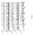
- FIG. 2 shows signal profiles in the switching relief network for power semiconductor switches according to FIG. 1, with an intermediate circuit voltage U D of 2800V, a cut-off relief capacitor C CL with a capacitance of 400 ⁇ F and a current limiting choke coil L CL with an inductance of 10 ⁇ H.
- the control method for the main converter with the power semiconductor switches V 11 to V 16 is triangular modulation with a triangular frequency f SW of 900 Hz and a modulation mod of 0.8.
- the load consists of a load inductance L load of 5 mH and a load resistance R load of 5 ⁇ .
- the oscillating circuit converter is controlled with a square wave signal with a switching frequency f RES of 8 kHz, a modulation mod RES of 0.5, an oscillating circuit inductance L RES of 250 ⁇ H and an oscillating circuit capacitance C RES of 1.5 ⁇ F.
- the current in the current limiting choke L CL with I L the current in the cut-off relief capacitor C CL with I C , the voltage difference across the resonant circuit converter with DU C , the current in the first semiconductor switch V res1 of the resonant circuit converter with I T1 and the voltage on the first semiconductor switch V res1 of the resonant circuit converter designated U T1 .
- the stresses on the components of the resonant circuit converter are illustrated in the expanded signal curves from FIG. 2 in FIG. 3.
- the semiconductor switches V res1 , V res2 of the resonant circuit converter are only stressed with the voltage difference DU C , which can be seen from FIGS. 2 and 3 below 100V. They work when switching on and off under zero current switching (ZCS) or zero current switching conditions.
- ZCS zero current switching
- FIGS. 4 and 5 are shown in FIGS. 4 and 5, FIG. 5 being an expanded representation of the signal curves according to FIG. 4.
- FIGS. 4 and 5 are shown in FIGS. 4 and 5, FIG. 5 being an expanded representation of the signal curves according to FIG. 4.
- the voltage applied to the resonant diode D R voltage U D shows a sinusoidal waveform and the resonance diode D R will only briefly conduct current I D, where it acts as a freewheeling diode for the resonant capacitor C res and prevents this is negatively charged. Due to the very slow rise in the cut-off voltage shown, the resonance diode D R has a soft cut-off behavior and is therefore only slightly stressed.
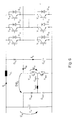
- FIG. 6 shows a further exemplary embodiment of the present invention, namely a switch-on relief network for power semiconductor switches with a resonant circuit converter arranged in parallel with the switch-off relief capacitor C CL , for feeding back the excess energy of the switch-off relief capacitor C CL .
- this circuit like the first exemplary embodiment of the invention described above with reference to FIGS. 1 to 5, is controlled independently of the control of the main converter V 11 to V 16 .
- the power semiconductor switches V 11 to V 16 together with their antiparallel reworking diodes D 11 to D 16 are part of a bridge circuit between a first pole of a DC voltage source, the connection of a Load, which is not shown in Fig. 6 and interconnects a second pole of the DC voltage source.
- a current limiting choke coil L CL is formed in the feed line of the first pole of the DC voltage source to the bridge circuit.
- a resonant circuit converter is arranged parallel to the cut-off relief capacitor C CL , which comprises two series-connected semiconductor switches V res1 , V res2 , which, starting from the connection point between the clamp diode D CL and the cut-off relief capacitor C CL , are connected to the second pole of the DC voltage source and each have an antiparallel feedback diode D res1 , D res2 , and a series resonant circuit a resonance capacitor C RES and a resonance choke coil L RES and the series connection of two resonance diodes D res3 , D res4 , which are poled starting from the second pole of the DC voltage source in the direction of the first pole of the DC voltage source and are connected in front of the current limiting choke coil L CL .
- the series resonant circuit L RES , C RES is connected to the connection point of the two semiconductor switches V res1 , V res2 and the connection point of the resonance diodes D res3
- the disadvantage of the switching relief network according to FIG. 6 compared to that according to FIG. 1 is that the semiconductor switches V res1 , V res2 are loaded with the full DC voltage source voltage U d because they are connected in parallel with the shutdown relief capacitor C CL .
- FIG. 7 shows waveforms in the switching relief circuit for power semiconductor switches according to FIG. 6 with an intermediate circuit voltage U d of 2800V, a clamp capacitor C CL with a capacitance of 400 ⁇ F and a current limiting inductance L CL of 10 ⁇ H.
- the control method for the main converter with the power semiconductor switches V 11 to V 16 is a triangular modulation with a triangular frequency f SW of 900 Hz, a modulation mod of 0.8, a load inductance L load of 5 mH and one Load resistance R load of 5 ⁇ .
- the resonant circuit converter is controlled with a square wave signal with a switching frequency f RES of 10 kHz, a modulation mod RES of 0.5, a resonant circuit inductance L RES of 100 ⁇ H and a resonant circuit capacitance C RES of 1 ⁇ F.
- a switching frequency f RES of 10 kHz a modulation mod RES of 0.5
- a resonant circuit capacitance C RES of 1 ⁇ F.
- the current in the current limiting inductor L CL with I L the current in the switch-off capacitor C CL with I C
- the voltage difference across the resonant circuit converter DU C the current in the first semiconductor switch V res1 of the resonant circuit converter with I T1 and the voltage on the semiconductor switch V res1 of the resonant circuit converter with U T1 .
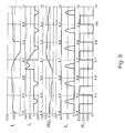
- the stresses on the components of the resonant circuit converter according to FIG. 6 are shown in FIG. 8 in extended signal profiles compared to the signal profiles from FIG. 7.
- the switching frequency f RES of the resonant circuit converter is selected to be lower than the resonant frequency of the resonant circuit L CL , C CL .
- the semiconductor switches V res1 , V res2 of the resonant circuit converter operate when switching on and off under zero current switching or zero current switching, which drastically reduces their switching losses.
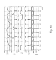
- FIGS. 9 and 10 show the same profiles as FIGS. 7 and 8, but in the partial load operation of the main converter (500/4 A).
- the switching frequency f RES of the resonant circuit converter has been reduced accordingly (10/4 kHz).
- the load current I L is approximately 200 A.
- the voltage difference DU C between the voltage U C at the clamp capacitor C CL and the intermediate circuit voltage U d remains below 50 V at this load current value, ie is halved compared to the previously discussed full-load operation.
- FIG. 11 A further development of the switching relief network according to the invention according to FIG. 1 is shown in FIG. 11.
- the clamp diode D CL which was connected in series with the cut-off relief capacitor C CL , is now replaced by three series circuits connected in parallel, each consisting of a clamp diode D CL and a snubber diode D SN .
- the diodes D CL and D SN are poled in the direction of the cut-off relief capacitor C CL .
- connection point between each clamp diode D CL and each snubber diode D SN is in each case via a snubber capacitor C SN , each with a connection point between two series-connected power semiconductor switches V 11 and V 12 , V 13 and V 14 or V 15 and V 16 and the respective connection of the load connected.
- FIG. 12 in turn shows a further development of the circuit according to the invention according to FIG. 11.
- the current limiting inductor L CL is now additionally replaced by three separate current limiting inductors connected in parallel.
- each connection point between a current limiting inductor L CL and an associated series connection of two power semiconductor switches V 11 and V 12 , V 13 and V 14 or V 15 and V 16 each with one of the series connections from the snubber diode D SN and the clamp Diode D CL connected.
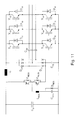
- FIG. 13 A corresponding development of the embodiment according to the invention according to FIG. 6 is shown in FIG. 13.
- the clamp diode D CL which was connected in series with the cut-off relief capacitor C CL , is now replaced by three parallel series connections, each consisting of a clamp diode D CL and a snubber diode D SN .
- the diodes D CL and D SN are poled in the direction of the cut-off relief capacitor C CL .
- the connection point between each clamp diode D CL and each snubber diode D SN is in each case connected via a snubber capacitor C SN to a connection point between two power semiconductor switches connected in series and the respective load connection.
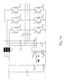
- FIG. 14 again shows a development of the circuit according to the invention according to FIG. 13.
- the current limiting choke coil L CL is now additionally divided into three separate current limiting choke coils.
- Each connection point between a current limiting inductor L CL and an associated series circuit comprising two power semiconductor switches V 11 and V 12 , V 13 and V 14 , V 15 and V 16 is then each with one of the series connections comprising the clamp diode D CL and a snubber diode D SN connected.
- the current limiting choke coil By dividing the current limiting choke coil into three individual coils, these are, as already described for the relief network according to FIG. 12, stressed with, for example, a factor of three smaller currents, which reduces the power loss per coil and simplifies the cooling of the coils.
- Another advantage is the decoupling achieved between the switching relief networks of the individual phases of the main converter. This prevents all switching operations within the main power converter from stressing all the snubber and clamp diodes.
- the controls of the circuit variants according to the invention are also very great easy to implement because they are independent of those of the power semiconductor switch of the main converter work.
- the level of the nominal operating overvoltage of the cut-off relief capacitor which is below 100 V, depends on the circuit variants according to the invention advantageously not from the regenerative converter, but only from the Height of the peak value of the load current and the capacitance of the cut-off relief capacitor from.
- Integrated bipolar transistors or bipolar transistors are currently preferred isolated gate electrode or IGBT as power semiconductor switch or Semiconductor switch used. It is also obvious to a person skilled in the art that also integrated gate commutated thyristors or IGCT and other power semiconductor switches used as a power semiconductor switch or semiconductor switch can be.
Landscapes
- Engineering & Computer Science (AREA)
- Power Engineering (AREA)
- Dc-Dc Converters (AREA)
Abstract
- Die Ansteuerung der Halbleiterschalter der Schwingkreisstromrichters ist unabhängig von der der Leistungshalbleiterschalter des Haupt-Stromrichters realisierbar.
- Die auftretende nominelle Betriebsüberspannung am Abschaltentlastungskondensator kann sehr klein gehalten werden, beispielsweise unter 100 V.
- Der Schaltungsaufwand ist verglichen mit herkömmlichen Schaltungen niedrig.
- Die Halbleiterschalter des Schwingkreisstromrichters werden unter Soft-Turn-On bzw. Einschaltentlastung und Soft-Turn-Off bzw. Abschaltentlastung betrieben (Resonanzbetrieb).
- Die Schaltung kann mit vertretbarem Aufwand für die Einschalt- und Abschaltentlastung des Hauptstromrichters erweitert werden.
- Die Ansteuerungen der erfindungsgemäßen Schaltungsvarianten sind zudem sehr einfach zu realisieren, da sie unabhängig von denen der Leistungshalbleiterschalter des Hauptstromrichters arbeiten.
Description
der zwei seriell verbundene Halbleiterschalter Vres1, Vres2 umfasst, die vom Verbindungspunkt zwischen Clamp-Diode DCL und Abschaltentlastungskondensator CCL ausgehend mit dem zweiten Pol der Gleichspannungsquelle verbunden sind und jeweils eine antiparallele Rückarbeitsdiode Dres1, Dres2 besitzen, sowie einen Reihenschwingkreis aus einem Resonanzkondensator CRES und einer Resonanzdrosselspule LRES und der Reihenschaltung zweier Resonanzdioden Dres3, Dres4, die vom zweiten Pol der Gleichspannungsquelle ausgehend in Richtung des ersten Poles der Gleichspannungsquelle gepolt und vor der Strombegrenzungsdrosselspule LCL angeschlossen sind. Der Reihenschwingkreis LRES, CRES ist mit dem Verbindungspunkt der zwei Halbleiterschalter Vres1, Vres2 und dem Verbindungspunkt der Resonanzdioden Dres3, Dres4 verbunden.
- Die Ansteuerung der Halbleiterschalter des Schwingkreisstromrichters ist unabhängig von der Leistungshalbleiterschalter des Hauptstromrichters realisierbar.
- Die nominelle Betriebsüberspannung des Abschaltentlastungskondensators kann sehr klein gehalten werden, beispielsweise unter 100 V, bei 3000V Gleichspannungsquellenspannung.
- Der Schaltungsaufwand ist verglichen mit herkömmlichen Schaltungen niedrig.
- Die Halbleiterschalter des Schwingkreisstromrichters werden unter Soft-Turn-On bzw. Einschaltentlastung und Soft-Turn-Off bzw. Abschaltentlastung betrieben (Resonanzbetrieb), dadurch werden sowohl Beanspruchungen durch Anstiege di/dt des Durchlassstromes beim Einschalten als auch Anstiege du/dt der Blokkierspannung beim Abschalten und die Abschaltüberspannung zuverlässig vermindert, so dass keine Schäden an den Bauelementen auftreten.
- Die Schaltung kann mit vertretbarem Aufwand für die Einschalt- und Abschaltentlastung der Leistungshalbleiterschalter des Haupt-Stromrichters erweitert werden.
Claims (9)
- Schaltentlastungsnetzwerk für Leistungshalbleiterschalter, mit:Leistungshalbleiterschaltern (V11 bis V16), die als Bestandteil einer Brückenschaltung zwischen einen ersten Pol einer Gleichspannungsquelle, den Anschlüssen einer Last und einen zweiten Pol der Gleichspannungsquelle, zusammen mit einer jedem Leistungshalbleiterschalter antiparallel geschalteten Rückarbeitsdioden (D11 bis D16) geschaltet sind,einer Strombegrenzungsdrosselspule (LCL) in der Zuleitung von der Gleichspannungsquelle zu den Leistungshalbleiterschalter (V11 bis V16 ),einem Abschaltentlastungskondensator (CCL) in Reihe mit einem Schwingkreisstromrichter, wobei der Schwingkreisstromrichter zur Rückführung der überschüssigen Energie des Abschaltentlastungskondensators (CCL) dient und unabhängig von den Leistungshalbleiterschaltern (V11 bis V16) ansteuerbar ist.
- Schaltentlastungsnetzwerk für Leistungshalbleiterschalter nach Anspruch 1, zusätzlich mit
einer zweiten, optionalen Strombegrenzungsdrosselspule in der Rückleitung zu dem zweiten Pol der Gleichspannungsquelle. - Schaltentlastungsnetzwerk für Leistungshalbleiterschalter nach Anspruch 1 oder 2, wobei
der Schwingkreisstromrichter eine in Richtung des Abschaltentlastungskondensators (CCL) gepolte Clamp-Diode (DCL), die mit dem Abschaltentlastungskondensator (CCL) in Reihe geschaltet ist, wobei diese Reihenschaltung diodenseitig mit der Verbindungsstelle der Leistungshalbleiterschalter (V11, V13 und V15) und der Einschaltentlastungsdrosselspule (LCL) und kondensatorseitig mit der Verbindungsstelle der Leistungshalbleiterschalter (V12, V14 und V16) mit der optionalen zweiten Strombegrenzungsdrosselspule oder dem zweiten Pol der Gleichspannungsquelle angeschlossen ist,
in Reihe verbundene erste und zweite Resonanz-Halbleiterschalter (Vres1, Vres2) jeweils mit antiparalleler Rückarbeitsdiode, wobei diese Reihenschaltung an den ersten Pol der Gleichspannungsquelle und einen Verbindungspunkt zwischen dem Abschaltentlastungskondensator (CCL) und der Clamp-Diode (DCL) angeschlossen ist, und
einen Reihenschwingkreis bestehend aus einer Resonanzdrosselspule (LRES) und einem Resonanzkondensator (CRES), wobei eine in Richtung der Resonanzdrosselspule (LRES) gepolte Resonanz-Diode (DRES) parallel zum Resonanzkondensator (CRES) geschaltet ist, wobei der Reihenschwingkreis an einem Verbindungspunkt zwischen dem ersten und zweiten Halbleiterschalter (Vres1, Vres2) und dem zweiten Pol der Gleichspannungsquelle angeschlossen ist, aufweist. - Schaltentlastungsnetzwerk für Leistungshalbleiterschalter, mit:Leistungshalbleiterschaltern (V11 bis V16), die als Bestandteil einer Brückenschaltung zwischen einen ersten Pol einer Gleichspannungsquelle, den Anschlüssen einer Last und einen zweiten Pol der Gleichspannungsquelle, zusammen mit einer jedem Leistungshalbleiterschalter antiparallel geschalteten Rückarbeitsdioden (D11 bis D16) geschaltet sind,einer Strombegrenzungsdrosselspule (LCL) in der Zuleitung von der Gleichspannungsquelle zu den Leistungshalbleitern (V11 bis V16),einem Abschaltentlastungskondensator (CCL) parallel zu einem Schwingkreisstromrichter, wobei der Schwingkreisstromrichter zur Rückführung der überschüssigen Energie des Abschaltentlastungskondensators (CCL) dient und unabhängig von den Leistungshalbleiterschaltern (V11 bis V16) ansteuerbar ist.
- Schaltentlastungsnetzwerk für Leistungshalbleiterschalter nach Anspruch 4, zusätzlich mit
einer optionalen, zweiten Strombegrenzungsdrosselspule in der Rückleitung zu dem zweiten Pol der Gleichspannungsquelle. - Schaltentlastungsnetzwerk für Leistungshalbleiterschalter nach Anspruch 4 oder 5, wobei
der Schwingkreisstromrichter eine in Richtung des Abschaltentlastungskondensators (CCL) gepolte Clamp-Diode (DCL), die mit dem Abschaltentlastungskondensator (CCL) in Reihe geschaltet ist, wobei die Reihenschaltung diodenseitig mit der Verbindungsstelle der Leistungshalbleiterschalter (V11, V13 und V15) und der Einschaltentlastungsdrosselspule (LCL) und kondensatorseitig mit der Verbindungsstelle der Leistungshalbleiterschalter (V12, V14 und V16) mit der optionalen zweiten Strombegrenzungsdrosselspule oder dem zweiten Pol der Gleichspannungsquelle angeschlossen ist,
in Reihe verbundene erste und zweite Halbleiterschalter (Vres1, Vres2) jeweils mit antiparalleler Rückarbeitsdiode, wobei diese Reihenschaltung an den zweiten Pol der Gleichspannungsquelle und einen Verbindungspunkt zwischen Clamp-Kondensator (CCL) und der Clamp-Diode (DCL) angeschlossen ist,
eine Reihenschaltung aus einer ersten und einer zweiten in Richtung auf den ersten Pol der Gleichspannungsquelle gepolten Resonanzdiode (Dres3, Dres4), wobei die Reihenschaltung zwischen dem ersten und dem zweiten Pol der Gleichspannungsquelle verbunden ist, und
einen Reihenschwingkreis bestehend aus einer Resonanz-Spule (LRES) und einem Resonanz-Kondensator (CRES), wobei der Reihenschwingkreis an einem Verbindungspunkt zwischen dem ersten und zweiten Halbleiterschalter (Vres1, Vres2) und dem Verbindungspunkt der ersten und der zweiten Resonanz-Diode (Dres3, Dres4) angeschlossen ist,
aufweist. - Schaltentlastungsnetzwerk nach einem der Ansprüche 1 bis 6, wobei
die Clamp-Diode (DCL) durch drei parallel geschaltete Reihenschaltungen jeweils aus einer Snubber-Diode (DSN) und einer Clamp-Diode (DCL) ersetzt ist, wobei die Snubber-Dioden (DSN) direkt mit dem Verbindungspunkt zwischen der Einschaltentlastungsdrosselspule (LCL) und den Leistungshalbleiterschaltern (V11, V13 und V15) verbunden sind, und der Verbindungspunkt zwischen jeder Clamp-Diode (DCL) und jeder Snubber-Diode (DSN) jeweils über einen Snubber-Kondensator (CSN) mit jeweils einem Verbindungspunkt zwischen zwei in Reihe geschalteten Leistungshalbleiterschaltern (V11 und V12, V13 und V14, V15 und V16) und dem jeweiligen Anschluss der Last verbunden ist. - Schaltentlastungsnetzwerk nach Anspruch 7, wobei
die Strombegrenzungsdrosselspule (LCL) durch drei parallel geschaltete Strombegrenzungsdrosselspulen (LCL) ersetzt ist, wobei jeder Verbindungspunkt zwischen einer Strombegrenzungsdrosselspule (LCL) und einer zugehörigen Reihenschaltung aus zwei Leistungshalbleiterschaltern (V11 und V12, V13 und V14, V15 und V16) mit jeweils einer der Reihenschaltungen aus der Clamp-Diode (DCL) und der weiteren Diode (DSN) verbunden ist. - Schaltentlastungsnetzwerk für Leistungshalbleiterschalter nach einem der vorangehenden Ansprüche 1 bis 8, wobei
die Leistungshalbleiterschalter (V11 bis V16) und/oder die ersten und zweiten Halbleiterschalter (Vres1, Vres2) durch Insulated Gate Bipolar Transistoren (IGBTs), Gate Turn Off Thyristoren (GTOs), Hard Driven Gate Turn Off Thyristoren (HDGTOs), Integrated Gate Commutated Tyhristoren (IGCTs) gebildet werden.
Applications Claiming Priority (2)
| Application Number | Priority Date | Filing Date | Title |
|---|---|---|---|
| DE10060766 | 2000-12-07 | ||
| DE10060766A DE10060766A1 (de) | 2000-12-07 | 2000-12-07 | Schaltentlastungsnetzwerk für Leistungshalbleiterschalter |
Publications (2)
| Publication Number | Publication Date |
|---|---|
| EP1213826A2 true EP1213826A2 (de) | 2002-06-12 |
| EP1213826A3 EP1213826A3 (de) | 2004-12-29 |
Family
ID=7666096
Family Applications (1)
| Application Number | Title | Priority Date | Filing Date |
|---|---|---|---|
| EP01250433A Withdrawn EP1213826A3 (de) | 2000-12-07 | 2001-12-07 | Schaltenlastungsnetzwerk für Leistungshalbleiterschalter |
Country Status (2)
| Country | Link |
|---|---|
| EP (1) | EP1213826A3 (de) |
| DE (1) | DE10060766A1 (de) |
Cited By (5)
| Publication number | Priority date | Publication date | Assignee | Title |
|---|---|---|---|---|
| WO2010000979A1 (fr) * | 2008-07-03 | 2010-01-07 | Sagem Defense Securite | Circuit d'amortissement actif pour un circuit electrique de decoupage |
| CN104638970A (zh) * | 2015-01-28 | 2015-05-20 | 华南理工大学 | 基于scc-lcl-t谐振网络的单相高频逆变器 |
| WO2017028989A1 (de) * | 2015-08-20 | 2017-02-23 | Robert Bosch Gmbh | Inverterschaltung mit einer schaltungsanordnung zum regenerativen dämpfen elektrischer schwingungen und verfahren zum regenerativen dämpfen elektrischer schwingungen |
| US10385509B2 (en) | 2015-05-01 | 2019-08-20 | The Procter & Gamble Company | Unitary deflection member for making fibrous structures having increased surface area and process for making same |
| EP4679697A1 (de) * | 2024-07-10 | 2026-01-14 | AmbiBox GmbH | Snubber für gleichspannungswandler |
Families Citing this family (1)
| Publication number | Priority date | Publication date | Assignee | Title |
|---|---|---|---|---|
| JP5679239B1 (ja) | 2013-08-27 | 2015-03-04 | 株式会社京三製作所 | 単相インバータ |
Family Cites Families (7)
| Publication number | Priority date | Publication date | Assignee | Title |
|---|---|---|---|---|
| DE4233573C2 (de) * | 1991-11-22 | 1994-04-28 | Licentia Gmbh | Selbstgeführter Stromrichter mit quasi-resonantem Gleichspannungs-Zwischenkreis |
| DE4303147C1 (de) * | 1993-01-30 | 1994-06-16 | Licentia Gmbh | GTO-Stromrichter mit quasi-resonantem Gleichspannungszwischenkreis |
| DE4447406C1 (de) * | 1994-12-24 | 1996-06-27 | Daimler Benz Ag | GTO-Stromrichter mit weicher Kommutierung |
| DE19636248C1 (de) * | 1996-08-28 | 1997-12-18 | Daimler Benz Ag | Verfahren zur Schaltentlastung eines IGBT |
| DE19730038C1 (de) * | 1997-07-14 | 1999-02-25 | Bosch Gmbh Robert | Anordnung zur Rückführung der Beschaltungsenergie bei einer Brückenschaltung |
| DE19735577C1 (de) * | 1997-08-09 | 1999-01-21 | Abb Daimler Benz Transp | Schaltungsanordnung zum entlasteten Schalten eines selbstgeführten Hochleistungs-Pulswechselrichters |
| US6111770A (en) * | 1997-10-28 | 2000-08-29 | Lockheed Martin Energy Research Corporation | Auxiliary resonant DC tank converter |
-
2000
- 2000-12-07 DE DE10060766A patent/DE10060766A1/de not_active Withdrawn
-
2001
- 2001-12-07 EP EP01250433A patent/EP1213826A3/de not_active Withdrawn
Cited By (13)
| Publication number | Priority date | Publication date | Assignee | Title |
|---|---|---|---|---|
| FR2933545A1 (fr) * | 2008-07-03 | 2010-01-08 | Sagem Defense Securite | Circuit d'amortissement actif pour circuit electrique de decoupage |
| CN102084580A (zh) * | 2008-07-03 | 2011-06-01 | 萨甘安全防护公司 | 电斩波电路用有源阻尼电路 |
| US8604860B2 (en) | 2008-07-03 | 2013-12-10 | Sagem Defense Securite | Active damping circuit for electric chopper circuit |
| CN102084580B (zh) * | 2008-07-03 | 2014-04-23 | 萨甘安全防护公司 | 电斩波电路用有源阻尼电路 |
| WO2010000979A1 (fr) * | 2008-07-03 | 2010-01-07 | Sagem Defense Securite | Circuit d'amortissement actif pour un circuit electrique de decoupage |
| CN104638970B (zh) * | 2015-01-28 | 2018-02-27 | 华南理工大学 | 基于scc‑lcl‑t谐振网络的单相高频逆变器 |
| CN104638970A (zh) * | 2015-01-28 | 2015-05-20 | 华南理工大学 | 基于scc-lcl-t谐振网络的单相高频逆变器 |
| US10385509B2 (en) | 2015-05-01 | 2019-08-20 | The Procter & Gamble Company | Unitary deflection member for making fibrous structures having increased surface area and process for making same |
| CN107960141A (zh) * | 2015-08-20 | 2018-04-24 | 罗伯特·博世有限公司 | 具有用于再生地衰减电振荡的线路布置的反相器线路和用于再生地衰减电振荡的方法 |
| WO2017028989A1 (de) * | 2015-08-20 | 2017-02-23 | Robert Bosch Gmbh | Inverterschaltung mit einer schaltungsanordnung zum regenerativen dämpfen elektrischer schwingungen und verfahren zum regenerativen dämpfen elektrischer schwingungen |
| US10608555B2 (en) | 2015-08-20 | 2020-03-31 | Robert Bosch Gmbh | Inverter circuit comprising a circuit arrangement for regenerative damping of electrical oscillations, and method for regenerative damping of electrical oscillations |
| CN107960141B (zh) * | 2015-08-20 | 2020-09-01 | 罗伯特·博世有限公司 | 具有用于再生地衰减电振荡的线路布置的反相器线路和用于再生地衰减电振荡的方法 |
| EP4679697A1 (de) * | 2024-07-10 | 2026-01-14 | AmbiBox GmbH | Snubber für gleichspannungswandler |
Also Published As
| Publication number | Publication date |
|---|---|
| DE10060766A1 (de) | 2002-06-13 |
| EP1213826A3 (de) | 2004-12-29 |
Similar Documents
| Publication | Publication Date | Title |
|---|---|---|
| DE102010008426B4 (de) | 3-Stufen-Pulswechselrichter mit Entlastungsnetzwerk | |
| EP2297842B1 (de) | Verfahren, schaltungsanordnung und brückenschaltung | |
| EP3523873B1 (de) | Gleichspannungswandler und verfahren zu dessen betrieb | |
| EP0852842A1 (de) | Verlustarmer leistungs-wechselrichter | |
| EP0969586A2 (de) | Dreipunkt-Stromrichter und Verfahren zum Betrieb | |
| DE102018210807A1 (de) | Elektrische Schaltung für Zero-Voltage-Soft-Switching in einem Gleichspannungswandler | |
| DE102010038511A1 (de) | Überspannungsschutzschaltung für mindestens einen Zweig einer Halbbrücke, Wechselrichter, Gleichspannungswandler und Schaltungsanordnung zum Betrieb einer elektrischen Maschine | |
| EP1213826A2 (de) | Schaltenlastungsnetzwerk für Leistungshalbleiterschalter | |
| EP3338351B1 (de) | Inverterschaltung mit einer schaltungsanordnung zum regenerativen dämpfen elektrischer schwingungen und verfahren zum regenerativen dämpfen elektrischer schwingungen | |
| DE3714175C2 (de) | ||
| DE3915510C2 (de) | ||
| DE102021213305B4 (de) | Drei-level-wandler mit aktivem angeschlossenem neutralpunkt und arcp entlastungsnetzwerk | |
| DE4447406C1 (de) | GTO-Stromrichter mit weicher Kommutierung | |
| DE4321988A1 (de) | Schaltungsanordnung für einen Zweipunkt-Wechselrichterschaltpol | |
| DE69814300T2 (de) | Stromwandler | |
| DE4042378C2 (de) | ||
| DE4430078A1 (de) | Schaltungsanordnung zur Vermeidung von Schaltverlusten eines Zweigpaares eines selbstgeführten Stromrichters mit eingeprägter Zwischenkreisgleichspannung | |
| EP3513475A1 (de) | Anlage zum übertragen elektrischer leistung mit filtereinheit | |
| EP3120447A1 (de) | Elektrische schaltung umfassend eine halbbrücke | |
| DE19527178C1 (de) | Rückspeiseschaltung für eine Entlastungsschaltung für einen Zweipunkt- bzw. Dreipunkt-Ventilzweig | |
| DE4106045C1 (en) | Multi-phase semiconductor three-stage AC inverter - has low inductance capacitors which limit sheet duration voltage transients | |
| EP2262087A1 (de) | Wandlerschaltung mit einem Umrichter | |
| DE3501925A1 (de) | Schaltungsanordnung fuer ein halbgesteuertes elektronisches zweigpaar | |
| DE102023111464A1 (de) | Umrichterschaltung | |
| DE3823399A1 (de) | Entlastungsnetzwerk fuer elektronische zweigpaare in antiparallelschaltung |
Legal Events
| Date | Code | Title | Description |
|---|---|---|---|
| PUAI | Public reference made under article 153(3) epc to a published international application that has entered the european phase |
Free format text: ORIGINAL CODE: 0009012 |
|
| AK | Designated contracting states |
Kind code of ref document: A2 Designated state(s): AT BE CH CY DE DK ES FI FR GB GR IE IT LI LU MC NL PT SE TR |
|
| AX | Request for extension of the european patent |
Free format text: AL;LT;LV;MK;RO;SI |
|
| PUAL | Search report despatched |
Free format text: ORIGINAL CODE: 0009013 |
|
| AK | Designated contracting states |
Kind code of ref document: A3 Designated state(s): AT BE CH CY DE DK ES FI FR GB GR IE IT LI LU MC NL PT SE TR |
|
| AX | Request for extension of the european patent |
Extension state: AL LT LV MK RO SI |
|
| AKX | Designation fees paid | ||
| REG | Reference to a national code |
Ref country code: DE Ref legal event code: 8566 |
|
| STAA | Information on the status of an ep patent application or granted ep patent |
Free format text: STATUS: THE APPLICATION IS DEEMED TO BE WITHDRAWN |
|
| 18D | Application deemed to be withdrawn |
Effective date: 20050701 |