EP1215524A2 - Illuminateur à lumière polarisée avec un diviseur de faisceau polarisant - Google Patents
Illuminateur à lumière polarisée avec un diviseur de faisceau polarisant Download PDFInfo
- Publication number
- EP1215524A2 EP1215524A2 EP01129139A EP01129139A EP1215524A2 EP 1215524 A2 EP1215524 A2 EP 1215524A2 EP 01129139 A EP01129139 A EP 01129139A EP 01129139 A EP01129139 A EP 01129139A EP 1215524 A2 EP1215524 A2 EP 1215524A2
- Authority
- EP
- European Patent Office
- Prior art keywords
- polarized light
- polarizing device
- light beam
- beam splitters
- integrator lens
- Prior art date
- Legal status (The legal status is an assumption and is not a legal conclusion. Google has not performed a legal analysis and makes no representation as to the accuracy of the status listed.)
- Withdrawn
Links
Images




Classifications
-
- G—PHYSICS
- G02—OPTICS
- G02F—OPTICAL DEVICES OR ARRANGEMENTS FOR THE CONTROL OF LIGHT BY MODIFICATION OF THE OPTICAL PROPERTIES OF THE MEDIA OF THE ELEMENTS INVOLVED THEREIN; NON-LINEAR OPTICS; FREQUENCY-CHANGING OF LIGHT; OPTICAL LOGIC ELEMENTS; OPTICAL ANALOGUE/DIGITAL CONVERTERS
- G02F1/00—Devices or arrangements for the control of the intensity, colour, phase, polarisation or direction of light arriving from an independent light source, e.g. switching, gating or modulating; Non-linear optics
- G02F1/01—Devices or arrangements for the control of the intensity, colour, phase, polarisation or direction of light arriving from an independent light source, e.g. switching, gating or modulating; Non-linear optics for the control of the intensity, phase, polarisation or colour
- G02F1/13—Devices or arrangements for the control of the intensity, colour, phase, polarisation or direction of light arriving from an independent light source, e.g. switching, gating or modulating; Non-linear optics for the control of the intensity, phase, polarisation or colour based on liquid crystals, e.g. single liquid crystal display cells
- G02F1/133—Constructional arrangements; Operation of liquid crystal cells; Circuit arrangements
- G02F1/1333—Constructional arrangements; Manufacturing methods
- G02F1/1337—Surface-induced orientation of the liquid crystal molecules, e.g. by alignment layers
-
- G—PHYSICS
- G02—OPTICS
- G02B—OPTICAL ELEMENTS, SYSTEMS OR APPARATUS
- G02B27/00—Optical systems or apparatus not provided for by any of the groups G02B1/00 - G02B26/00, G02B30/00
- G02B27/28—Optical systems or apparatus not provided for by any of the groups G02B1/00 - G02B26/00, G02B30/00 for polarising
- G02B27/283—Optical systems or apparatus not provided for by any of the groups G02B1/00 - G02B26/00, G02B30/00 for polarising used for beam splitting or combining
-
- G—PHYSICS
- G02—OPTICS
- G02B—OPTICAL ELEMENTS, SYSTEMS OR APPARATUS
- G02B27/00—Optical systems or apparatus not provided for by any of the groups G02B1/00 - G02B26/00, G02B30/00
- G02B27/09—Beam shaping, e.g. changing the cross-sectional area, not otherwise provided for
- G02B27/0927—Systems for changing the beam intensity distribution, e.g. Gaussian to top-hat
-
- G—PHYSICS
- G02—OPTICS
- G02B—OPTICAL ELEMENTS, SYSTEMS OR APPARATUS
- G02B27/00—Optical systems or apparatus not provided for by any of the groups G02B1/00 - G02B26/00, G02B30/00
- G02B27/09—Beam shaping, e.g. changing the cross-sectional area, not otherwise provided for
- G02B27/0938—Using specific optical elements
- G02B27/095—Refractive optical elements
- G02B27/0955—Lenses
-
- G—PHYSICS
- G02—OPTICS
- G02F—OPTICAL DEVICES OR ARRANGEMENTS FOR THE CONTROL OF LIGHT BY MODIFICATION OF THE OPTICAL PROPERTIES OF THE MEDIA OF THE ELEMENTS INVOLVED THEREIN; NON-LINEAR OPTICS; FREQUENCY-CHANGING OF LIGHT; OPTICAL LOGIC ELEMENTS; OPTICAL ANALOGUE/DIGITAL CONVERTERS
- G02F1/00—Devices or arrangements for the control of the intensity, colour, phase, polarisation or direction of light arriving from an independent light source, e.g. switching, gating or modulating; Non-linear optics
- G02F1/01—Devices or arrangements for the control of the intensity, colour, phase, polarisation or direction of light arriving from an independent light source, e.g. switching, gating or modulating; Non-linear optics for the control of the intensity, phase, polarisation or colour
- G02F1/13—Devices or arrangements for the control of the intensity, colour, phase, polarisation or direction of light arriving from an independent light source, e.g. switching, gating or modulating; Non-linear optics for the control of the intensity, phase, polarisation or colour based on liquid crystals, e.g. single liquid crystal display cells
- G02F1/133—Constructional arrangements; Operation of liquid crystal cells; Circuit arrangements
- G02F1/1333—Constructional arrangements; Manufacturing methods
- G02F1/1337—Surface-induced orientation of the liquid crystal molecules, e.g. by alignment layers
- G02F1/13378—Surface-induced orientation of the liquid crystal molecules, e.g. by alignment layers by treatment of the surface, e.g. embossing, rubbing or light irradiation
- G02F1/133788—Surface-induced orientation of the liquid crystal molecules, e.g. by alignment layers by treatment of the surface, e.g. embossing, rubbing or light irradiation by light irradiation, e.g. linearly polarised light photo-polymerisation
Definitions
- the invention relates to a polarized light illuminator in which an alignment layer of a liquid crystal cell element and a wide view film which is built into the liquid crystal cell are irradiated with polarized light.
- a liquid crystal cell element is produced as follows:
- optical alignment For the above described alignment treatment of the alignment layer of a liquid crystal cell element, there is a technique which is called "optical alignment".
- an alignment layer is irradiated with polarized light and exposed.
- a polarized light illuminator is disclosed, for example, in Japanese patent specification 2928226 and Japanese patent specification 2960392 (both corresponding to published European Patent Application EP 0 913 720 A2 and U.S. Patent 6190016).
- a wide view film is produced as follows:
- the reduction in image quality can be equalized by cementing a wide view film onto the liquid crystal cell.
- the polarizing device which is used for the above described illuminator to have resistance to heat and strong light.
- several glass plates are tilted with respect to the optical axis by the Brewster angle and located parallel to one another with distances (hereinafter called a "pile polarization plate").
- the invention was devised to eliminate the above described disadvantages of the prior art.
- primary objects of the present invention are to reduce the size of a polarizing device used for a polarized light illuminator, to cut the costs of the polarizing device and to reduce the size of the entire polarized light illuminator.
- a polarized light beam splitter can be imagined as a polarizing device which has resistance to heat and strong light.
- a polarized light beam splitter is produced by vacuum evaporation of an inorganic, dielectric, multi-layer film (which serves as a polarization separating film) onto the inclined surface of a right-angled prism, and by cementing the inclined surfaces of two right-angle prisms to one another.
- the unpolarized light incident in the polarized light beam splitter is separated into P-polarized and S-polarized light by the inorganic, dielectric, multi-layer film.
- the P-polarized light propagates in a straight line and is transmitted by the beam splitter.
- the S-polarized light is reflected. Since the prism is made of quartz glass, it is resistant to heat and strong light.
- the inorganic, dielectric, multi-layer film which is a polarization separation film made of an inorganic material, it has resistance to heat and strong light. Furthermore, an inorganic, dielectric, multi-layer film can be produced which, at a predetermined wavelength, has a good polarization separation characteristic (which has a good extinction ratio, for example, a small portion of the S-polarized light in the transmitted polarized P-polarized light).
- the irradiation area becomes larger, by which the device becomes larger and also a large polarizing device is needed.
- the size of the prisms comprising the polarized light beam splitter is, however, limited for reasons of production, such as due to the size of the vacuum evaporation device which forms the vacuum evaporated film. Furthermore, the costs of the quartz prism become very high when the prism becomes large.
- a polarizing device is formed by combination of several of these polarized light beam splitters with one another.
- combining small prisms yields a large polarizing device.
- an application for optical alignment of a large liquid crystal cell element is enabled and the costs can also be reduced.
- the length of the polarizing device can be reduced in the direction of the optical axis, the illuminator can be made smaller.
- the polarized light beam splitters are arranged such that the shadow formed by the areas of the boundary surfaces of the polarized light beam splitters is projected onto the boundary lines between several combined lenses of the integrator lens.
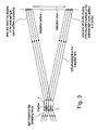
- the boundary surfaces between the respective lenses of the integrator lens are shadowy due to light irradiation. However, these shadows are projected onto the outer side of the irradiation area. Therefore, when the shadow of the boundary surfaces of the polarized light beam splitters is projected onto the boundary lines between the respective lens of the integrator lens, the shadows are prevented from being projected onto the irradiation surface by the boundary surfaces of the polarized light beam splitters.
- the illuminance of the light which emerges from the outer peripheral edge area on the respective outlet side of the respective lens of the several lenses which form the integrator lens is reduced more than the illuminance of the light which emerges from the middle area.
- the above described areas in which the illuminance decreases are projected onto the outside of the irradiation area.
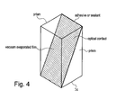
- an adhesive or sealant is used to cement the inclined surfaces of two right-angled prisms to one another.
- commercial adhesives or sealants absorb UV light and are damaged over time when they are irradiated with UV light with the wavelength which is used for optical alignment (currently with respect to the material for the alignment layer, often with a wavelength from 200 nm to 340 nm). In this way, the transmittance of the UV light is reduced. Therefore, to cement the polarized light beam splitters, an "optical contact" is used, and thus, joining takes place, but “optical contact” is easily lost by the influences of temperature changes and humidity.
- a polarized light illuminator In a polarized light illuminator, it is necessary to keep the properties, such as the extinction ratio of the emitted polarized light and the like, stable over a long time.
- the adhesive surfaces of the polarized light beam splitters become loose, the polarization characteristic decreases. Therefore, an adhesive or sealant is applied to the vicinity of the cemented surfaces and the humidity is prevented from being absorbed by the inner sides of the adhesive surfaces. Thus, the connection strength is maintained.
- Figure 1 is a schematic representation of the entire arrangement of an embodiment of a polarized light illuminator in accordance with the invention
- Figure 2 schematically depicts an embodiment in which there is a polarizing device on the light incidence side of the integrator lens
- Figure 3 is a schematic representation of the action of the integrator lens
- Figure 4 schematically represents cementing of the prisms of a polarized light beam splitter
- Figures 5(a) & 5(b) each show a schematic of an embodiment in which the integrator lens and the polarized light beam splitter are combined with one another;
- Figure 6 shows a schematic of a sample arrangement in which the integrator lens and the polarized light beam splitter are combined with one another;
- Figure 7 shows a schematic of an embodiment in which there is an optical element (a convex lens) on the incidence side of the polarizing device;
- Figure 8 is a schematic representation of an embodiment in which there is a polarizing device on the outlet side of an integrator lens.
- Figure 9 schematically depicts a conventional example in which a pile polarization plate is used as the polarizing device.
- FIG. 1 shows the overall arrangement of an embodiment of a polarized light illuminator in accordance with the invention.
- the light which is emitted from a lamp 1 and which contains UV radiation is focused by an oval focusing mirror 2, reflected by a first planar mirror 3 and is incident on an optical unit 10 comprised of a polarizing device 5 and an integrator lens 4.
- the polarizing device 5 is formed by combination of several polarized light beam splitters, as was described above.
- the integrator lens 4 in which on the outlet side of the polarizing device 5, as is described below.
- the polarizing device 5 transmits the P-polarized light and reflects most of the S-polarized light. Therefore, the light which is incident on the integrator lens 4 becomes mostly P-polarized light which is passed through a shutter 6 and reflected by means of a second planar mirror 7, converted into parallel light by means of a collimator 8 and emitted onto a workpiece W, such as a substrate or the like which has been placed on the workpiece carrier 9.
- optical unit 10 comprises the above described integrator lens 4 and the above described polarizing device 5.
- Figure 2 shows an embodiment in which the polarizing device 5 is located on the light incidence side of the integrator lens 4.
- the light is incident from a light source on the polarizing device 5 which is formed of several polarized light beam splitters 5a, is subjected to polarization separation and is incident on the integrator lens 4.
- the polarized light emerging from the integrator lens 4 is emitted via an optical element, such as a reflector or the like, onto the irradiation surface, as was described above.
- the polarizing device 5 is formed by a combination of several polarized light beam splitters 5a, in the areas of the combination surfaces (boundary surfaces) of the several polarized light beam splitters 5a, a shadow which is projected onto the irradiation surface is formed when the combination surfaces of the several polarized light beam splitters 5a are irradiated with light. In this way, a reduction in the illuminance and a deterioration of the distribution of the illuminance are caused.
- the polarizing device 5 and the integrator lens 4 are shown arranged at a distance from one another to show the shadow of the boundary surfaces of the polarized light beam splitters 5a.
- the two are brought into contact with one another, the shadow of the boundary surfaces of the polarized light beam splitters 5a is projected onto the boundary surfaces of the integrator lens 4 without broadening.
- the areas in which the illuminance is reduced becomes smaller.
- polarized light beam splitter 5a two prisms are connected to one another via a vacuum evaporated film. Since degradation by UV light occurs when an adhesive is applied to the joining surface, as was described above, they are joined to one another with "optical contact". "Optical contact” is described, for example, in Japanese patent disclosure document HEI 9-5518 and Japanese patent disclosure document HEI 10-142408.
- the size and the arrangement of the individual polarized light beam splitter can also be matched to the size and arrangement of the respective lenses 4a which form the integrator lens 4, as shown in Figure 5(a).
- Figure 5(b) using rod-shaped polarized light beam splitters 5a, their boundary surfaces can be positioned in the shadow areas of the boundary surfaces of the lens group 4a on the light incidence side.
- several polarized light beam splitters 5a with suitable sizes can be combined with one another. In this case, if the irradiation area is rectangular, the shape of the individual lenses 4a comprising the integrator lens 4 can be made rectangular and thus a rectangular polarized light beam splitter can be used. This also applies to the following embodiments.
- a polarizing device 5 which was formed by combining several polarized light beam splitters 5a, the size of the prisms of the individual polarized light beam splitter can be reduced and can be suitably adjusted to the device for irradiating large surfaces, and moreover, the production costs can be reduced. Furthermore, the length of the polarizing device in the direction of the optical axis can be reduced and therefore the illuminator can be made smaller.
- the arrangement in which the shadow of the boundary surfaces of several polarized light beam splitters 5a is projected onto the boundary lines between the several lenses 4a which form the integrator lens 4 prevents the shadow of the boundary lines of the polarized light beam splitters 5a from being projected onto the irradiation surface.
- the decrease in illuminance and the deterioration of the distribution of the illuminance can be prevented.
- the polarized light beam splitters 5a are produced according to the shape and size of the individual lenses comprising the integrator lens 4, and are located next to one another according to the arrangement of the above described individual lenses. If parallel light is allowed to be incident on the polarizing device 5 (this means that, in this case, the optical path lengths run parallel to one another), the shadow can be projected by the boundary surfaces of the polarized light beam splitters 5a onto the boundary surfaces of the integrator lens 4 in a more suitable manner.
- the optical path lines can be allowed to be incident on the polarizing device 5 in parallel, and thus, the shadow can be suitably projected by the boundary surfaces of the polarized light beam splitters 5a onto the boundary surfaces of the integrator lens 4 in a suitable manner. Furthermore, the disadvantages that the proportion of unpolarized light in the outer peripheral area of the irradiation area increases and that the illuminance of the polarized light is reduced can be eliminated.
- the polarizing device can also be located on the outlet side of the integrator lens.
- a pre-stage lens convex lens
- a post-stage lens concave lens
- Figure 8 shows an embodiment in which the polarizing device is on the outlet side of the integrator lens.
- the light from the light source (not shown in the drawings) is incident on the integrator lens 4.
- the respective optical path lines are made parallel to one another and are incident on the middle of the respective polarized light beam splitters 5a comprising the polarizing device 5. They are incident on the polarizing device 5, that is formed of several polarized light beam splitters 5a, and are subjected to polarization separation.
- the polarized light from the polarizing device 5 is incident on the post-stage lens 13, is converted into nonparallel scattered light, and emitted via an optical element, such as a reflector or the like, onto the irradiation surface, as described above.
- the illuminance of the light which emerges from the outer peripheral edge area on the respective outlet side of the respective lens of the several lenses which form the integrator lens is reduced more than the illuminance of the light which emerges from the middle area, when light is incident on the integrator lens.
- the areas in which the illuminance has been reduced are projected onto the outside of the irradiation area.
- the polarized light beam splitters 5a are arranged such that the boundary surfaces of the polarized light beam splitters 5a are positioned in the areas in which the illuminance decreases, that is, the outer peripheral edge areas of the several lenses which form the integrator lens 4 (of the boundary surfaces between the respective lenses). In this way, as was described using Figure 3, the shadow areas of the boundary surfaces of the polarized light beam splitters 5a are prevented from being projected onto the irradiation area.
- the boundary surfaces of the polarized light beam splitters are positioned in the shadow areas of the integrator lens.
- the size and the arrangement of the individual polarized light beam splitter can also be matched to the size and arrangement of the individual lenses 4a which form the integrator lens, as shown in above in Figures 5(a), 5(b) & 6.
- an arrangement using rod-shaped polarized light beam splitters can be undertaken or several polarized light beam splitters with suitable sizes can be combined with one another.
- the light emerging from the integrator lens 4 is scattered light, as is shown in Figure 8, and it broadens during incidence on the pre-stage lens 12 according to the distance between the two.
- the size of the individual polarized light beam splitter 5a which is located downstream of the pre-stage lens 12 must therefore be matched to the broadening of the light emerging from the integrator lens 4 so that the areas of the outer peripheral edge areas of the above described several lenses in which the illuminance decreases and the boundary surfaces of the polarized light beam splitters 5a agree with one another, and thus, the shadow of the boundary surfaces of the polarized light beam splitters 5a is not projected onto the irradiation area.
- the individual polarized light beam splitters 5a are, as described in the first embodiment, joined to one another with "optical contact" and the entire periphery of the joining surfaces is covered with an adhesive or sealant. Since the boundary surface areas of the polarized light beam splitters 5a to which the adhesive or sealant is applied are located in the areas in which the illuminance of the light emerging from the integrator lens 4 decreases, the adhesive or sealant is degraded. If it is assumed that the adhesive or sealant is degraded by scattered light or the like, there is no effect on the illuminance of the irradiation surface because this area is an area which is projected to outside the irradiation area.
Landscapes
- Physics & Mathematics (AREA)
- General Physics & Mathematics (AREA)
- Optics & Photonics (AREA)
- Nonlinear Science (AREA)
- Crystallography & Structural Chemistry (AREA)
- Chemical & Material Sciences (AREA)
- Mathematical Physics (AREA)
- Spectroscopy & Molecular Physics (AREA)
- Polarising Elements (AREA)
- Projection Apparatus (AREA)
- Microscoopes, Condenser (AREA)
- Exposure And Positioning Against Photoresist Photosensitive Materials (AREA)
- Optical Elements Other Than Lenses (AREA)
Applications Claiming Priority (2)
| Application Number | Priority Date | Filing Date | Title |
|---|---|---|---|
| JP2000377170 | 2000-12-12 | ||
| JP2000377170A JP2002182158A (ja) | 2000-12-12 | 2000-12-12 | 偏光ビームスプリッタを備えた光配向用偏光光照射装置 |
Publications (2)
| Publication Number | Publication Date |
|---|---|
| EP1215524A2 true EP1215524A2 (fr) | 2002-06-19 |
| EP1215524A3 EP1215524A3 (fr) | 2004-03-17 |
Family
ID=18845935
Family Applications (1)
| Application Number | Title | Priority Date | Filing Date |
|---|---|---|---|
| EP01129139A Withdrawn EP1215524A3 (fr) | 2000-12-12 | 2001-12-07 | Illuminateur à lumière polarisée avec un diviseur de faisceau polarisant |
Country Status (5)
| Country | Link |
|---|---|
| US (1) | US6724530B2 (fr) |
| EP (1) | EP1215524A3 (fr) |
| JP (1) | JP2002182158A (fr) |
| KR (1) | KR20020046148A (fr) |
| TW (1) | TWI225953B (fr) |
Cited By (1)
| Publication number | Priority date | Publication date | Assignee | Title |
|---|---|---|---|---|
| RU2676867C1 (ru) * | 2015-02-02 | 2019-01-11 | Телефонактиеболагет Лм Эрикссон (Пабл) | Использование информации о луче антенны |
Families Citing this family (12)
| Publication number | Priority date | Publication date | Assignee | Title |
|---|---|---|---|---|
| US20050134825A1 (en) * | 2002-02-08 | 2005-06-23 | Carl Zeiss Smt Ag | Polarization-optimized illumination system |
| US7344254B2 (en) * | 2003-03-28 | 2008-03-18 | Thomson Licensing | Projection system with a common light source sharing system |
| AU2003255441A1 (en) * | 2003-08-14 | 2005-03-29 | Carl Zeiss Smt Ag | Illuminating device for a microlithographic projection illumination system |
| JP4797468B2 (ja) | 2004-07-07 | 2011-10-19 | 大日本印刷株式会社 | 位相差制御部材、その製造方法、及び液晶ディスプレイ装置 |
| JP2006215684A (ja) * | 2005-02-02 | 2006-08-17 | Furukawa Electric Co Ltd:The | 侵入検知パネル及び光導波路装着方法 |
| EP2009678A4 (fr) * | 2006-04-17 | 2011-04-06 | Nikon Corp | Appareil optique d'éclairage, appareil d'exposition, et procédé de fabrication du dispositif |
| JP5012002B2 (ja) * | 2006-12-25 | 2012-08-29 | 凸版印刷株式会社 | 近接露光方法 |
| JP2010087388A (ja) * | 2008-10-02 | 2010-04-15 | Ushio Inc | 露光装置 |
| JP6391921B2 (ja) * | 2013-07-30 | 2018-09-19 | 浜松ホトニクス株式会社 | 波長板及び分割プリズム部材 |
| KR102235338B1 (ko) * | 2014-09-03 | 2021-04-05 | 삼성디스플레이 주식회사 | 곡면형 액정표시패널 제조방법 및 곡면형 액정표시패널 제조설비 |
| CN108345180B (zh) * | 2017-01-25 | 2020-04-10 | 上海微电子装备(集团)股份有限公司 | 一种曝光和光配向一体的装置及其使用方法 |
| CN112817168A (zh) * | 2019-11-15 | 2021-05-18 | 苏州大学 | 成像检测组件 |
Family Cites Families (23)
| Publication number | Priority date | Publication date | Assignee | Title |
|---|---|---|---|---|
| US2748659A (en) * | 1951-02-26 | 1956-06-05 | Jenaer Glaswerk Schott & Gen | Light source, searchlight or the like for polarized light |
| US2821114A (en) * | 1952-04-16 | 1958-01-28 | Pola Lux Ges Fur Blendschutz A | Symmetrical interference polarizers |
| JP3273955B2 (ja) * | 1991-04-09 | 2002-04-15 | キヤノン株式会社 | 画像投影装置 |
| WO1996020422A1 (fr) * | 1994-12-28 | 1996-07-04 | Seiko Epson Corporation | Appareil d'eclairage en lumiere polarisee et dispositif d'affichage du type a projection |
| JPH08334616A (ja) | 1995-06-09 | 1996-12-17 | Olympus Optical Co Ltd | 偏光プリズム |
| JPH095518A (ja) | 1995-06-19 | 1997-01-10 | Nikon Corp | 偏光ビームスプリッター及びその製造方法 |
| JPH09304734A (ja) * | 1996-05-15 | 1997-11-28 | Seiko Epson Corp | 偏光照明装置および投写型表示装置 |
| WO1997045768A1 (fr) * | 1996-05-29 | 1997-12-04 | Seiko Epson Corporation | Dispositif d'affichage par projection |
| US6404550B1 (en) * | 1996-07-25 | 2002-06-11 | Seiko Epson Corporation | Optical element suitable for projection display apparatus |
| US6109752A (en) * | 1996-08-26 | 2000-08-29 | Seiko Epson Corporation | Lighting device and projector |
| JPH10142408A (ja) | 1996-11-12 | 1998-05-29 | Canon Inc | 光学素子の製造方法及び該方法による光学素子 |
| KR19990076941A (ko) * | 1996-11-28 | 1999-10-25 | 이데이 노부유끼 | 광학블록과 표시장치 |
| KR100228430B1 (ko) * | 1996-12-30 | 1999-11-01 | 김영환 | 액정표시소자의 배향막 처리장치 및 이를 이용한 배향막 처리 방법 |
| EP0867734B1 (fr) * | 1997-03-28 | 2005-06-08 | Seiko Epson Corporation | Système optique d'illumination et dispositif d'affichage du type projection |
| US6292296B1 (en) * | 1997-05-28 | 2001-09-18 | Lg. Philips Lcd Co., Ltd. | Large scale polarizer and polarizer system employing it |
| US6067193A (en) * | 1997-10-15 | 2000-05-23 | Nikon Corporation | Polarization device and projection type display apparatus |
| TW536644B (en) * | 1997-10-29 | 2003-06-11 | Ushio Electric Inc | Polarized light radiation device for alignment film of liquid crystal display element |
| JPH11142850A (ja) * | 1997-11-05 | 1999-05-28 | Hitachi Ltd | 偏光照射方法とその装置 |
| JPH11183848A (ja) * | 1997-12-17 | 1999-07-09 | Seiko Epson Corp | 偏光照明装置および投写型表示装置 |
| JPH11218724A (ja) * | 1998-01-29 | 1999-08-10 | Fuji Photo Optical Co Ltd | 照明用光学系およびこれを用いた液晶プロジェクタ装置 |
| JP3384346B2 (ja) * | 1999-01-14 | 2003-03-10 | ウシオ電機株式会社 | 液晶表示素子の光配向用偏光光照射装置 |
| JP3622556B2 (ja) * | 1999-02-23 | 2005-02-23 | セイコーエプソン株式会社 | 照明光学系および投写型表示装置 |
| JP3817970B2 (ja) | 1999-05-31 | 2006-09-06 | ウシオ電機株式会社 | 偏光ビームスプリッタおよびそれを用いた液晶表示素子の配向膜光配向用偏光光照射装置 |
-
2000
- 2000-12-12 JP JP2000377170A patent/JP2002182158A/ja active Pending
-
2001
- 2001-10-04 TW TW090124565A patent/TWI225953B/zh not_active IP Right Cessation
- 2001-11-15 KR KR1020010070987A patent/KR20020046148A/ko not_active Ceased
- 2001-12-07 EP EP01129139A patent/EP1215524A3/fr not_active Withdrawn
- 2001-12-11 US US10/011,429 patent/US6724530B2/en not_active Expired - Fee Related
Cited By (1)
| Publication number | Priority date | Publication date | Assignee | Title |
|---|---|---|---|---|
| RU2676867C1 (ru) * | 2015-02-02 | 2019-01-11 | Телефонактиеболагет Лм Эрикссон (Пабл) | Использование информации о луче антенны |
Also Published As
| Publication number | Publication date |
|---|---|
| KR20020046148A (ko) | 2002-06-20 |
| TWI225953B (en) | 2005-01-01 |
| EP1215524A3 (fr) | 2004-03-17 |
| US6724530B2 (en) | 2004-04-20 |
| US20020080485A1 (en) | 2002-06-27 |
| JP2002182158A (ja) | 2002-06-26 |
Similar Documents
| Publication | Publication Date | Title |
|---|---|---|
| KR100454692B1 (ko) | 액정표시소자의배향막광배향용편광광조사장치 | |
| JP4063042B2 (ja) | 光配向用偏光光照射装置 | |
| US6724530B2 (en) | Polarized light illuminator with a polarized light beam splitter | |
| US6190016B1 (en) | Irradiation device for an alignment layer of a liquid crystal cell element | |
| CN101943800A (zh) | 偏振转换装置及其制造方法 | |
| EP1172684B1 (fr) | Dispositif d'irradiation à lumière polarisée pour une couche d'alignement pour dispositif d'affichage à cristaux liquide | |
| KR20010010649A (ko) | 광투사형 디스플레이장치의 편광변환소자 | |
| EP1162491A2 (fr) | Appareil d'irradiation par la lumière polarisée | |
| CN100386664C (zh) | 偏振转换光学系统 | |
| JP2005300886A (ja) | 液晶表示素子の製造方法および光配向用偏光光照射装置 | |
| EP1020739A2 (fr) | Dispositif d'irradiation de lumière polarisée pour l'alignement d'un élément d'affichage à cristaux liquides | |
| JPH11194344A (ja) | 液晶表示素子の配向膜光配向用偏光光照射装置 | |
| US20020080486A1 (en) | Polarized light illuminator for optical alignment | |
| JPH10161126A (ja) | 配向膜の形成方法および露光装置 | |
| JP2001056451A (ja) | 照明装置およびそれを用いた投写型表示装置 | |
| JPH0572417A (ja) | 偏光変換素子 | |
| JP2000147506A (ja) | 光照射装置 | |
| US6652111B2 (en) | Irradiation device for polarized light for optical alignment of a liquid crystal cell element | |
| KR20040100869A (ko) | 광 배향용 편광광 조사 장치 | |
| US6081377A (en) | Polarized light synthesizing device and display device using the same | |
| JP3319729B2 (ja) | 偏光光源装置 | |
| JPH08271836A (ja) | 偏光方向整列素子 |
Legal Events
| Date | Code | Title | Description |
|---|---|---|---|
| PUAI | Public reference made under article 153(3) epc to a published international application that has entered the european phase |
Free format text: ORIGINAL CODE: 0009012 |
|
| AK | Designated contracting states |
Kind code of ref document: A2 Designated state(s): AT BE CH CY DE DK ES FI FR GB GR IE IT LI LU MC NL PT SE TR |
|
| AX | Request for extension of the european patent |
Free format text: AL;LT;LV;MK;RO;SI |
|
| PUAL | Search report despatched |
Free format text: ORIGINAL CODE: 0009013 |
|
| AK | Designated contracting states |
Kind code of ref document: A3 Designated state(s): AT BE CH CY DE DK ES FI FR GB GR IE IT LI LU MC NL PT SE TR |
|
| AX | Request for extension of the european patent |
Extension state: AL LT LV MK RO SI |
|
| RIC1 | Information provided on ipc code assigned before grant |
Ipc: 7H 04N 9/31 B Ipc: 7G 02B 27/28 B Ipc: 7G 02B 27/00 A |
|
| AKX | Designation fees paid | ||
| REG | Reference to a national code |
Ref country code: DE Ref legal event code: 8566 |
|
| STAA | Information on the status of an ep patent application or granted ep patent |
Free format text: STATUS: THE APPLICATION IS DEEMED TO BE WITHDRAWN |
|
| 18D | Application deemed to be withdrawn |
Effective date: 20040918 |