EP1217648A2 - Verfahren zur Herstellung einer dielektrischen Zwischenschicht mit niedriger Dielektrizitätskonstante - Google Patents
Verfahren zur Herstellung einer dielektrischen Zwischenschicht mit niedriger Dielektrizitätskonstante Download PDFInfo
- Publication number
- EP1217648A2 EP1217648A2 EP01123338A EP01123338A EP1217648A2 EP 1217648 A2 EP1217648 A2 EP 1217648A2 EP 01123338 A EP01123338 A EP 01123338A EP 01123338 A EP01123338 A EP 01123338A EP 1217648 A2 EP1217648 A2 EP 1217648A2
- Authority
- EP
- European Patent Office
- Prior art keywords
- film
- insulating film
- semiconductor device
- forming
- manufacturing
- Prior art date
- Legal status (The legal status is an assumption and is not a legal conclusion. Google has not performed a legal analysis and makes no representation as to the accuracy of the status listed.)
- Withdrawn
Links
Images



Classifications
-
- H—ELECTRICITY
- H10—SEMICONDUCTOR DEVICES; ELECTRIC SOLID-STATE DEVICES NOT OTHERWISE PROVIDED FOR
- H10P—GENERIC PROCESSES OR APPARATUS FOR THE MANUFACTURE OR TREATMENT OF DEVICES COVERED BY CLASS H10
- H10P14/00—Formation of materials, e.g. in the shape of layers or pillars
- H10P14/60—Formation of materials, e.g. in the shape of layers or pillars of insulating materials
- H10P14/69—Inorganic materials
- H10P14/692—Inorganic materials composed of oxides, glassy oxides or oxide-based glasses
- H10P14/6921—Inorganic materials composed of oxides, glassy oxides or oxide-based glasses containing silicon
- H10P14/6922—Inorganic materials composed of oxides, glassy oxides or oxide-based glasses containing silicon the material containing Si, O and at least one of H, N, C, F or other non-metal elements, e.g. SiOC, SiOC:H or SiONC
- H10P14/6927—Inorganic materials composed of oxides, glassy oxides or oxide-based glasses containing silicon the material containing Si, O and at least one of H, N, C, F or other non-metal elements, e.g. SiOC, SiOC:H or SiONC the material being a silicon oxynitride, e.g. SiON or SiON:H
-
- C—CHEMISTRY; METALLURGY
- C23—COATING METALLIC MATERIAL; COATING MATERIAL WITH METALLIC MATERIAL; CHEMICAL SURFACE TREATMENT; DIFFUSION TREATMENT OF METALLIC MATERIAL; COATING BY VACUUM EVAPORATION, BY SPUTTERING, BY ION IMPLANTATION OR BY CHEMICAL VAPOUR DEPOSITION, IN GENERAL; INHIBITING CORROSION OF METALLIC MATERIAL OR INCRUSTATION IN GENERAL
- C23C—COATING METALLIC MATERIAL; COATING MATERIAL WITH METALLIC MATERIAL; SURFACE TREATMENT OF METALLIC MATERIAL BY DIFFUSION INTO THE SURFACE, BY CHEMICAL CONVERSION OR SUBSTITUTION; COATING BY VACUUM EVAPORATION, BY SPUTTERING, BY ION IMPLANTATION OR BY CHEMICAL VAPOUR DEPOSITION, IN GENERAL
- C23C16/00—Chemical coating by decomposition of gaseous compounds, without leaving reaction products of surface material in the coating, i.e. chemical vapour deposition [CVD] processes
- C23C16/22—Chemical coating by decomposition of gaseous compounds, without leaving reaction products of surface material in the coating, i.e. chemical vapour deposition [CVD] processes characterised by the deposition of inorganic material, other than metallic material
- C23C16/30—Deposition of compounds, mixtures or solid solutions, e.g. borides, carbides, nitrides
- C23C16/40—Oxides
- C23C16/401—Oxides containing silicon
-
- C—CHEMISTRY; METALLURGY
- C23—COATING METALLIC MATERIAL; COATING MATERIAL WITH METALLIC MATERIAL; CHEMICAL SURFACE TREATMENT; DIFFUSION TREATMENT OF METALLIC MATERIAL; COATING BY VACUUM EVAPORATION, BY SPUTTERING, BY ION IMPLANTATION OR BY CHEMICAL VAPOUR DEPOSITION, IN GENERAL; INHIBITING CORROSION OF METALLIC MATERIAL OR INCRUSTATION IN GENERAL
- C23C—COATING METALLIC MATERIAL; COATING MATERIAL WITH METALLIC MATERIAL; SURFACE TREATMENT OF METALLIC MATERIAL BY DIFFUSION INTO THE SURFACE, BY CHEMICAL CONVERSION OR SUBSTITUTION; COATING BY VACUUM EVAPORATION, BY SPUTTERING, BY ION IMPLANTATION OR BY CHEMICAL VAPOUR DEPOSITION, IN GENERAL
- C23C16/00—Chemical coating by decomposition of gaseous compounds, without leaving reaction products of surface material in the coating, i.e. chemical vapour deposition [CVD] processes
- C23C16/44—Chemical coating by decomposition of gaseous compounds, without leaving reaction products of surface material in the coating, i.e. chemical vapour deposition [CVD] processes characterised by the method of coating
- C23C16/50—Chemical coating by decomposition of gaseous compounds, without leaving reaction products of surface material in the coating, i.e. chemical vapour deposition [CVD] processes characterised by the method of coating using electric discharges
- C23C16/505—Chemical coating by decomposition of gaseous compounds, without leaving reaction products of surface material in the coating, i.e. chemical vapour deposition [CVD] processes characterised by the method of coating using electric discharges using radio frequency discharges
- C23C16/509—Chemical coating by decomposition of gaseous compounds, without leaving reaction products of surface material in the coating, i.e. chemical vapour deposition [CVD] processes characterised by the method of coating using electric discharges using radio frequency discharges using internal electrodes
- C23C16/5096—Flat-bed apparatus
-
- H—ELECTRICITY
- H10—SEMICONDUCTOR DEVICES; ELECTRIC SOLID-STATE DEVICES NOT OTHERWISE PROVIDED FOR
- H10P—GENERIC PROCESSES OR APPARATUS FOR THE MANUFACTURE OR TREATMENT OF DEVICES COVERED BY CLASS H10
- H10P14/00—Formation of materials, e.g. in the shape of layers or pillars
- H10P14/60—Formation of materials, e.g. in the shape of layers or pillars of insulating materials
- H10P14/66—Formation of materials, e.g. in the shape of layers or pillars of insulating materials characterised by the type of materials
- H10P14/662—Laminate layers, e.g. stacks of alternating high-k metal oxides
-
- H—ELECTRICITY
- H10—SEMICONDUCTOR DEVICES; ELECTRIC SOLID-STATE DEVICES NOT OTHERWISE PROVIDED FOR
- H10P—GENERIC PROCESSES OR APPARATUS FOR THE MANUFACTURE OR TREATMENT OF DEVICES COVERED BY CLASS H10
- H10P14/00—Formation of materials, e.g. in the shape of layers or pillars
- H10P14/60—Formation of materials, e.g. in the shape of layers or pillars of insulating materials
- H10P14/69—Inorganic materials
- H10P14/692—Inorganic materials composed of oxides, glassy oxides or oxide-based glasses
- H10P14/6921—Inorganic materials composed of oxides, glassy oxides or oxide-based glasses containing silicon
- H10P14/69215—Inorganic materials composed of oxides, glassy oxides or oxide-based glasses containing silicon the material being a silicon oxide, e.g. SiO2
-
- H—ELECTRICITY
- H10—SEMICONDUCTOR DEVICES; ELECTRIC SOLID-STATE DEVICES NOT OTHERWISE PROVIDED FOR
- H10W—GENERIC PACKAGES, INTERCONNECTIONS, CONNECTORS OR OTHER CONSTRUCTIONAL DETAILS OF DEVICES COVERED BY CLASS H10
- H10W20/00—Interconnections in chips, wafers or substrates
- H10W20/01—Manufacture or treatment
- H10W20/071—Manufacture or treatment of dielectric parts thereof
- H10W20/074—Manufacture or treatment of dielectric parts thereof of dielectric parts comprising thin functional dielectric layers, e.g. dielectric etch-stop, barrier, capping or liner layers
- H10W20/075—Manufacture or treatment of dielectric parts thereof of dielectric parts comprising thin functional dielectric layers, e.g. dielectric etch-stop, barrier, capping or liner layers of multilayered thin functional dielectric layers
-
- H—ELECTRICITY
- H10—SEMICONDUCTOR DEVICES; ELECTRIC SOLID-STATE DEVICES NOT OTHERWISE PROVIDED FOR
- H10W—GENERIC PACKAGES, INTERCONNECTIONS, CONNECTORS OR OTHER CONSTRUCTIONAL DETAILS OF DEVICES COVERED BY CLASS H10
- H10W20/00—Interconnections in chips, wafers or substrates
- H10W20/01—Manufacture or treatment
- H10W20/071—Manufacture or treatment of dielectric parts thereof
- H10W20/074—Manufacture or treatment of dielectric parts thereof of dielectric parts comprising thin functional dielectric layers, e.g. dielectric etch-stop, barrier, capping or liner layers
- H10W20/077—Manufacture or treatment of dielectric parts thereof of dielectric parts comprising thin functional dielectric layers, e.g. dielectric etch-stop, barrier, capping or liner layers on sidewalls or on top surfaces of conductors
-
- H—ELECTRICITY
- H10—SEMICONDUCTOR DEVICES; ELECTRIC SOLID-STATE DEVICES NOT OTHERWISE PROVIDED FOR
- H10P—GENERIC PROCESSES OR APPARATUS FOR THE MANUFACTURE OR TREATMENT OF DEVICES COVERED BY CLASS H10
- H10P14/00—Formation of materials, e.g. in the shape of layers or pillars
- H10P14/60—Formation of materials, e.g. in the shape of layers or pillars of insulating materials
- H10P14/63—Formation of materials, e.g. in the shape of layers or pillars of insulating materials characterised by the formation processes
- H10P14/6326—Deposition processes
- H10P14/6328—Deposition from the gas or vapour phase
- H10P14/6334—Deposition from the gas or vapour phase using decomposition or reaction of gaseous or vapour phase compounds, i.e. chemical vapour deposition
- H10P14/6336—Deposition from the gas or vapour phase using decomposition or reaction of gaseous or vapour phase compounds, i.e. chemical vapour deposition in the presence of a plasma [PECVD]
-
- H—ELECTRICITY
- H10—SEMICONDUCTOR DEVICES; ELECTRIC SOLID-STATE DEVICES NOT OTHERWISE PROVIDED FOR
- H10P—GENERIC PROCESSES OR APPARATUS FOR THE MANUFACTURE OR TREATMENT OF DEVICES COVERED BY CLASS H10
- H10P14/00—Formation of materials, e.g. in the shape of layers or pillars
- H10P14/60—Formation of materials, e.g. in the shape of layers or pillars of insulating materials
- H10P14/66—Formation of materials, e.g. in the shape of layers or pillars of insulating materials characterised by the type of materials
- H10P14/665—Porous materials
-
- H—ELECTRICITY
- H10—SEMICONDUCTOR DEVICES; ELECTRIC SOLID-STATE DEVICES NOT OTHERWISE PROVIDED FOR
- H10P—GENERIC PROCESSES OR APPARATUS FOR THE MANUFACTURE OR TREATMENT OF DEVICES COVERED BY CLASS H10
- H10P14/00—Formation of materials, e.g. in the shape of layers or pillars
- H10P14/60—Formation of materials, e.g. in the shape of layers or pillars of insulating materials
- H10P14/66—Formation of materials, e.g. in the shape of layers or pillars of insulating materials characterised by the type of materials
- H10P14/668—Formation of materials, e.g. in the shape of layers or pillars of insulating materials characterised by the type of materials the materials being characterised by the deposition precursor materials
- H10P14/6681—Formation of materials, e.g. in the shape of layers or pillars of insulating materials characterised by the type of materials the materials being characterised by the deposition precursor materials the precursor containing a compound comprising Si
- H10P14/6682—Formation of materials, e.g. in the shape of layers or pillars of insulating materials characterised by the type of materials the materials being characterised by the deposition precursor materials the precursor containing a compound comprising Si the compound being a silane, e.g. disilane, methylsilane or chlorosilane
-
- H—ELECTRICITY
- H10—SEMICONDUCTOR DEVICES; ELECTRIC SOLID-STATE DEVICES NOT OTHERWISE PROVIDED FOR
- H10P—GENERIC PROCESSES OR APPARATUS FOR THE MANUFACTURE OR TREATMENT OF DEVICES COVERED BY CLASS H10
- H10P14/00—Formation of materials, e.g. in the shape of layers or pillars
- H10P14/60—Formation of materials, e.g. in the shape of layers or pillars of insulating materials
- H10P14/66—Formation of materials, e.g. in the shape of layers or pillars of insulating materials characterised by the type of materials
- H10P14/668—Formation of materials, e.g. in the shape of layers or pillars of insulating materials characterised by the type of materials the materials being characterised by the deposition precursor materials
- H10P14/6681—Formation of materials, e.g. in the shape of layers or pillars of insulating materials characterised by the type of materials the materials being characterised by the deposition precursor materials the precursor containing a compound comprising Si
- H10P14/6684—Formation of materials, e.g. in the shape of layers or pillars of insulating materials characterised by the type of materials the materials being characterised by the deposition precursor materials the precursor containing a compound comprising Si the compound comprising silicon and oxygen
- H10P14/6686—Formation of materials, e.g. in the shape of layers or pillars of insulating materials characterised by the type of materials the materials being characterised by the deposition precursor materials the precursor containing a compound comprising Si the compound comprising silicon and oxygen the compound being a molecule comprising at least one silicon-oxygen bond and the compound having hydrogen or an organic group attached to the silicon or oxygen, e.g. a siloxane
-
- H—ELECTRICITY
- H10—SEMICONDUCTOR DEVICES; ELECTRIC SOLID-STATE DEVICES NOT OTHERWISE PROVIDED FOR
- H10P—GENERIC PROCESSES OR APPARATUS FOR THE MANUFACTURE OR TREATMENT OF DEVICES COVERED BY CLASS H10
- H10P14/00—Formation of materials, e.g. in the shape of layers or pillars
- H10P14/60—Formation of materials, e.g. in the shape of layers or pillars of insulating materials
- H10P14/69—Inorganic materials
- H10P14/692—Inorganic materials composed of oxides, glassy oxides or oxide-based glasses
- H10P14/6921—Inorganic materials composed of oxides, glassy oxides or oxide-based glasses containing silicon
- H10P14/6922—Inorganic materials composed of oxides, glassy oxides or oxide-based glasses containing silicon the material containing Si, O and at least one of H, N, C, F or other non-metal elements, e.g. SiOC, SiOC:H or SiONC
Definitions
- the present invention relates to a semiconductor device in which an interlayer insulating film having a low dielectric constant is formed by covering wiring primarily made of a copper film, and to a method of manufacturing the same.
- a low dielectric insulating film that has a low dielectric constant for small RC delay (hereinafter referred to as a low dielectric insulating film) is used.
- a plasma enhanced CVD method that uses trimethylsilane (SiH(CH 3 ) 3 ) and N 2 O is known as one method.
- SiH(CH 3 ) 3 trimethylsilane
- N 2 O a plasma enhanced CVD method that uses trimethylsilane (SiH(CH 3 ) 3 ) and N 2 O.
- Si(CH 3 ) 4 trimethylsilane
- Si(CH 3 ) 4 tetramethylsilane
- N 2 O description is made in "J. Shi, M. A-Plano, T. Mountsier, and S. Nag, SEMICON Korea Technical Symposium 2000, p.279 (2000)” and the like.
- the low dielectric insulating film formed by the above-mentioned methods is relatively weak in adhesion strength with wiring primarily made of a copper film and is low in film hardness. Improvements are therefore expected.
- An object of the present invention is to provide a method of manufacturing a semiconductor device capable of forming an insulating film that has a low dielectric constant, the insulating film also having a good adhesion property with wiring primarily made of a copper film and appropriate film hardness, and a semiconductor device produced by the method.
- film forming is performed by adjusting pressure of a film-forming gas. Specifically, film forming is performed under low gas pressure at an initial stage of film forming, then under high gas pressure for the remainder.
- the invention has a step of forming an insulating film (hereinafter, referred to as a low-pressure insulating film) on a substrate by converting a film-forming gas into a plasma state under the gas pressure below 1 Torr for reaction, and a step of forming an insulating film (hereinafter, referred to as a high-pressure insulating film) on the low-pressure insulating film by converting a film-forming gas formed into a plasma state under the gas pressure of 1 Torr or higher for reaction.
- a low-pressure insulating film a low-pressure insulating film
- exfoliation intensity between the substrate and the insulating film is inversely proportional to the gas pressure of the film-forming gas.
- the exfoliation intensity rises extremely high under gas pressure below 1 Torr.
- the dielectric constant of the formed film is high in the film formed under low gas pressure, and low in the film formed under high gas pressure.
- film forming is performed by reaction with the film-forming gas of low gas pressure converted into a plasma state at the initial stage of film forming, thereafter, film forming is performed by converting the film-forming gas of high gas pressure into plasma for reaction, whereby an insulating film with high adhesion and of a low dielectric constant as a whole can be formed.
- film forming is performed on a silicon substrate, however, the same result may be obtained in a case when film forming is performed on a copper substrate.
- the barrier insulating film is formed by the method of manufacturing a semiconductor device of the present invention. Specifically, initial film forming is performed so as to form a low-pressure insulating film, and the remainder is formed as a high-pressure insulating film. As for a frequency of electric power for forming plasma, a low frequency is set for both the low-pressure insulating film and the high-pressure insulating film.
- film forming with electric power of a low frequency imparts strong adhesion force, however, the adhesion strength even increases more when film forming is performed by use of a film-forming gas of low pressure at the initial stage of the film forming.
- a nitrogen-containing gas such as ammonia (NH 3 ) or nitrogen (N 2 ) as a film-forming gas of a barrier insulating film improves a barrier property.
- nitrogen (N 2 ) an inert gas such as helium (He) or argon (Ar) or the like, the film-forming gas can be diluted without losing the adhesion force of the formed film.
- the foregoing invention is applied to a method of forming a barrier insulating film as a base for the main insulating film and a main insulating film having a low dielectric constant.
- the gas pressure does not have to be changed during the film forming.
- FIG. 1 is a side view showing a constitution of a plasma film-forming apparatus used for a method of manufacturing a semiconductor device according to an embodiment of the present invention.
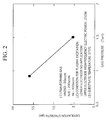
- FIG. 2 is a graph showing a relation of exfoliation intensity to gas pressure of a film-forming gas for a low dielectric insulating film according to a first embodiment of the present invention.
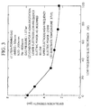
- FIG. 3 is a graph showing a relation of exfoliation intensity to low-frequency electric power for substrate bias in the event that the film-forming gas for the low dielectric insulating film according to the first embodiment of the present invention is converted into plasma.
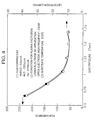
- FIG. 4 is a graph showing relations of film hardness and Young's modulus to the gas pressure of the film-forming gas for the low dielectric insulating film according to the first embodiment of the present invention.
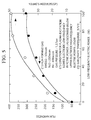
- FIG. 5 is a graph showing relations of film hardness and Young's modulus to the low-frequency electric power for substrate bias in the event that the film-forming gas for the low dielectric insulating film according to the first embodiment of the present invention is converted into plasma.
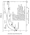
- FIG. 6 is a graph showing relations, each of a relative dielectric constant to the low-frequency electric power for substrate bias in the event that the film-forming gas for the low dielectric insulating film according to the first embodiment of the present invention is converted into plasma.
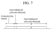
- FIG. 7 is a view showing procedures of film forming according to the first embodiment of the present invention.
- FIG. 8A and FIG. 8B are cross-sectional views showing a semiconductor device and a method of manufacturing the same according to a second embodiment of the present invention.
- FIG. 9A and FIG. 9B are cross-sectional views showing a semiconductor device and a method of manufacturing the same according to a third and a fourth embodiments of the present invention.
- FIG.1 is a side view showing a configuration of the parallel-plate type plasma enhanced CVD film forming apparatus 101 employed in a film forming method according to an embodiment of the present invention.
- This plasma enhanced CVD film forming apparatus 101 comprises a film forming portion 101A that is the place at which a silicon-containing insulating film is formed by the plasma gas on a substrate 21 subject to a film formation (hereinbelow, referred to as a substrate), and a film forming gas supplying portion 101B having a plurality of gas supply sources constituting the film forming gas.
- the film forming portion 101A has a chamber 1 whose pressure can be reduced, and the chamber 1 is connected to an exhausting device 6 via an exhaust pipe 4.
- a switching valve 5 for controlling the open and the close between the chamber 1 and the exhausting device 6 is provided in the middle of the exhaust pipe 4.
- a pressure measuring means such as a vacuum gauge (not shown) for monitoring the pressure in the chamber 1 is provided to the chamber 1.
- a pair of opposing upper electrode (second electrode) 2 and lower electrode (first electrode) 3 are provided to the chamber 1.
- a high frequency power supply (RF power supply) 7 for supplying a high frequency power having a frequency of 13.56 MHz is connected to the upper electrode 2
- a low frequency electric power supply 8 for supplying a low frequency electric power having a frequency of 380 kHz is connected to the lower electrode 3.
- the film forming gas is plasmanized by supplying the power to the upper electrode 2 and the lower electrode 3 from these power supplies 7, 8.
- the upper electrode 2, the lower electrode 3, and the power supplies 7, 8 constitute the plasma generating means for plasmanizing the film forming gas.
- the upper electrode 2 is also used as a film forming gas distributor.
- a plurality of through holes are formed in the upper electrode 2, and opening portions of the through holes in the surface opposing to the lower electrode 3 serve as discharge ports (inlet ports) of the film forming gas.
- the discharge ports of the film forming gas, etc. are connected to the film forming gas supplying portion 101B via a pipe 9a.
- a heater (not shown) may be provided to the upper electrode 2, as the case may be. This is because, if the upper electrode 2 is heated at the temperature of almost 100 °C during the film formation, particles made of reaction products of the film forming gas, etc. can be prevented from sticking onto the upper electrode 2.
- the lower electrode 3 is also used as a loading table for the substrate 21.
- a heater 12 for heating the substrate 21 on the loading table is provided to the lower electrode 3.
- switching means 10u to 10z for controlling the open and the close between the branch pipe 9j, that is connected to the N 2 gas supply source, and remaining branch pipes 9b to 9e, 9g, 9h are provided.
- the N 2 gas purges the residual gas in the pipe 9a and the chamber 1 in addition to the branch pipes 9b to 9e, 9g, 9h.
- the N 2 gas also is employed as a diluting gas as the case may be.
- the supply source for supplying the alkyl compound having siloxane bond the supply source for supplying the hydrocarbon, the supply source for supplying the oxygen-containing gas and the supply source for supplying the inert gas are provided, and also the plasma generating means 2, 3, 7, 8 for plasmanizing the film forming gas are provided.
- the exhausting device 6 and flow rate controlling means 11a to 11i are provided.
- a means for generating a plasma by the upper and lower electrodes 2, 3 of parallel-plate type is employed as a plasma generating means, and the power supplies 7, 8 for supplying the powers having two high and low frequencies are connected to the upper and lower electrodes 2, 3 respectively. Therefore, the plasma can be generated by applying the powers having these two high and low frequencies to the electrodes 2, 3 respectively.
- the insulating film formed in this manner is dense, and the insulating film has a low dielectric constant as CH 3 is contained in the insulating film.
- a low frequency electric power of 100kHz or more and less than 1 MHz is applied to the lower electrode 3, or the low frequency electric power is applied to the lower electrode 3 and a high frequency electric power of 1MHz or more is applied to the upper electrode 2.
- a high frequency electric power is applied to the upper electrode 2.
- the low frequency electric power is applied to the lower electrode 3 in addition to applying the high frequency electric power to the upper electrode 2.
- the low frequency electric power of 100kHz or more and less than 1 MHz is applied to the lower electrode 3, and in a process of forming a high-pressure insulating film, the low frequency electric power is applied to the lower electrode 3.
- the high frequency power may be applied to the upper electrode 2.
- the alkyl compound having the siloxane bond the methyl silane, the hydrocarbon, the oxygen containing gas and the diluting gas as the film forming gas to which the present invention is applied, followings may be employed as the typical examples.
- a silicon insulating film was formed on a Si substrate using plasma enhanced CVD method (PE-CVD method) under the following film forming condition.
- the HMDSO was employed as the alkyl compound having siloxane bond, the N 2 O as the oxygen containing gas, and the He as the diluting gas.
- one minute and thirty seconds are taken as a period (a stabilizing period) for substitution of gases in the chamber from the gas introduction to the chamber to a start of the film formation, and the upper electrode 2 is heated at 100 °C to prevent reaction products from sticking to the upper electrode 2.
- FIG. 2 is a view showing a relation between gas pressure of a film-forming gas and exfoliation intensity of a film formed on a silicon substrate.
- the axis of ordinates thereof shows the exfoliation intensity (gw) of a formed film scaled by linear graduations, and the axis of abscissas thereof shows the gas pressure (Torr) of a film-forming gas scaled by linear graduations.
- Insulating films for examination were formed on silicon substrates in accordance with the parameters of the above-described conditions for film forming except that application of the low-frequency electric power to the lower electrode 3 was not carried out, and under two conditions of the gas pressure of the film-forming gas by 0.9 and 1.5 Torr, respectively.
- the exfoliation intensity was measured by use of a measurement instrument made by Shimadzu Corporation (Shimadzu Scanning Scratch Tester SST101.)
- the exfoliation intensity which was in the range from 5 to 6 gw in the case of the gas pressure of 1.5 Torr, was significantly improved in the case of the gas pressure of 0.9 Torr by nearly three times, which was in the range from 15 to 16 gw.
- FIG. 3 is a view showing a relation between low-frequency electric power of the plasma-excited condition applied to the lower electrode 3 and exfoliation intensity of a film formed on a silicon substrate.
- the axis of ordinates thereof shows the exfoliation intensity (gw) of a formed film scaled by linear graduations, and the axis of abscissas thereof shows the low-frequency electric power (W) scaled by linear graduations.
- Insulating films for examination were formed on silicon substrates in accordance with the above-described conditions for film forming while setting the gas pressure of the film-forming gas to 1.5 Torr, and under six conditions of the low-frequency electric power of 0, 10, 30, 50, 75 and 100 W, respectively.
- the same measurement instrument as in the case (a) was used.
- the exfoliation intensity decreased as the electric power increased, such as from some 6 gw at 0 W to some 3.3 gw at 30 W.
- the exfoliation intensity did not decrease significantly, and was settled around 3 gw.
- FIG. 4 is a view showing relations between gas pressure of a film-forming gas and film hardness as well as Young's modulus of a film formed on a silicon substrate.
- the left axis of ordinates thereof shows the film hardness of a formed film scaled by linear graduations, while the right axis of ordinates shows Young's modulus (GP) of the formed film scaled by linear graduations.
- the axis of abscissas shows the gas pressure (Torr) of a film-forming gas scaled by linear graduations.
- Insulating films for examination were formed on silicon substrates in accordance with the above-described conditions for film forming except that application of the low-frequency electric power to the lower electrode 3 was not carried out, and under six conditions of the gas pressure of the film-forming gas of 0.7, 0.9, 1.1, 1.3, 1.5 and 1.7 Torr, respectively.
- the film hardness and Young's modulus were measured by use of a measurement instrument made by Shimadzu Corporation (Shimadzu Dynamic Ultra Micro Hardness Tester DUH-W201S).
- the film hardness decreases as the gas pressure increases.
- the film hardness was about 230 when the gas pressure was 0.7 Torr, and around 70 to 80 when the gas pressure was 1.3 Torr.
- the film hardness did not significantly change any more, and was settled around 50.
- Young's modulus also showed a tendency substantially similar to that of the film hardness. Young's modulus was about 40 GP when the gas pressure was 0.7 Torr, and it was about 10 GP when the gas pressure was 1.3 Torr. When the gas pressure exceeded 1.3 Torr, Young's modulus was settled around 10 GP.
- FIG. 5 is a view showing relations between low-frequency electric power applied to the lower electrode 3 for forming direct current bias voltage to a substrate subject to film forming, and film hardness as well as Young's modulus of a film formed on a silicon substrate.
- the left axis of ordinates thereof shows the film hardness of a formed film scaled by linear graduations, while the right axis of ordinates shows Young's modulus (GP) of the formed film scaled by linear graduations.
- the axis of abscissas shows the low-frequency electric power (W) scaled by linear graduations.
- Insulating films for examination were formed on silicon substrates in accordance with the above-described conditions for film forming while setting the gas pressure of the film-forming gas to 1.5 Torr, and under six conditions of the low-frequency electric power of 0, 10, 30, 50, 75 and 100 W, respectively.
- the same measurement instrument as in the case (c) was used.
- the film hardness increases along with an increase of the electric power.
- the increase of the film hardness becomes gentle.
- the film hardness was about 50 when the low-frequency electric power was not applied, about 290 at 75 W, and about 300 at 100 W.
- Young's modulus also showed a tendency similar to that of the film hardness. Young's modulus was about 8 GP when the low-frequency electric power was not applied, about 47 GP at 75 W, and about 50 at 100 W.
- FIG. 6 is a view showing relations, each between low-frequency electric power applied to the lower electrode 3 for forming direct current bias voltage to a substrate subject to film forming and a relative dielectric constant of a film formed on a silicon substrate.
- the axis of ordinates thereof shows the relative dielectric constant of a formed film scaled by linear graduations.
- the axis of abscissas shows the low-frequency electric power (W) scaled by linear graduations.
- Insulating films for examination were formed on silicon substrates in accordance with the above-described conditions for film forming under three conditions of the gas pressure of the film-forming gas by 0.9, 1.2 and 1.5 Torr, respectively, and under six conditions of the low-frequency electric power of 0, 10, 20, 50, 75 and 100 W, respectively.
- the relative dielectric constants were measured by the C-V method, in which a signal of a frequency of 1 MHz is superposed on a direct current bias.
- the relative dielectric constant sharply increases in a range of the low-frequency electric power from 0 to 20 W, which was observed as ranging from about 2.9 to 4.3.
- the relative dielectric constant then gently decreases as the low-frequency electric power further increases beyond 20 W.
- the relative dielectric constant sharply increases in a range of the low-frequency electric power from 0 to 20 W, which was observed as ranging from about 2.7 to 3.9.
- the relative dielectric constant gently increases beyond 20 W to be about 4.8 at 100 W.
- the relative dielectric constant sharply increases in a range of the low-frequency electric power from 0 to 20 W, which was observed as ranging from about 2.7 to 3.6.
- the relative dielectric constant gently increases beyond 20 W to be about 4.1 at 100 W.
- the exfoliation intensity is large when the pressure is low, however, the relative dielectric constant becomes high.
- the exfoliation intensity is large at lower than 1 Torr, and the relative dielectric constant is low at 1 Torr or higher.
- the exfoliation intensity becomes high and the relative dielectric constant becomes low when the electric power is low.
- the gas pressure will be adjusted for a low-pressure insulating film and a high-pressure insulating film as similarly to the case of forming the interlayer insulating film, while a frequency of the electric power for plasma excitation will not be adjusted but maintained to a low frequency for both the low-pressure insulating film as well as the high-pressure insulating film.
- the gas pressure such as below 1 Torr for example, and to lower the low-frequency electric power in an initial stage of film-forming, thus enhancing exfoliation intensity at a little sacrifice of a relative dielectric constant, then for the remainder, to perform film forming with gas pressure of 1 Torr or higher for example, thus lowering the relative dielectric constant of the entire film.
- gas pressure below 1 Torr is preferable at the initial stage of film forming
- the gas pressure below 0.1 Torr brings a slow film-forming rate hence it is not practical.
- the gas pressure of 1 Torr or higher is preferable for forming the rest of the film
- the gas pressure within the maximum of 10 Torr is practical in light of electrical discharge.
- FIG. 8A and FIG. 8B Next, a semiconductor device and a method of manufacturing the same according to a second embodiment of the present invention will be described with reference to the FIG. 8A and FIG. 8B.
- FIG 8A is a cross-sectional view showing a semiconductor device produced by the method of manufacturing a semiconductor device according to the second embodiment of the present invention.
- FIG. 8B is a cross-sectional view of FIG. 8A taken along a line I-I.
- a film-forming gas composed of HMDSO + N 2 O + He is used in order to form an interlayer insulating film 34 between wiring-embedded films, the interlayer insulating film being sandwiched a lower wiring-embedded insulating film 32 where lower wiring 33 is embedded and an upper wiring-embedded insulating film 35 where upper wiring 37 is embedded.
- the wiring-embedded insulating film 32 is formed on a base substrate 31, the wiring-embedded insulating film being composed of either a SiO 2 film or a SiOCH film in a film thickness of about 1 ⁇ m. It should be noted that the SiOCH film is an insulating film that contains Si, O, C and H.
- a wiring groove is formed by etching the wiring-embedded insulating film 32, thereafter a TaN film 33a is formed inside the wiring groove as a anti-diffusion film for copper.
- an unillustrated copper seed layer is formed on a surface of the TaN film 33a by a sputtering method, then a copper film is embedded by a plating method.
- the copper film and the TaN film 33a projected from the wiring groove are then subjected to polishing by a chemical mechanical polishing (CMP) method, thus the surface of the lower wiring is planarized.
- CMP chemical mechanical polishing
- the interlayer insulating film 34 between wiring-embedded films composed of a PE-CVD SiOCH film in a film thickness of several tens of nanometers, is formed by a plasma enhanced CVD method using HMDSO + N 2 O + He. Detail description thereof will be made hereunder.
- a substrate 21 is introduced to a chamber 1 of a film-forming apparatus 101, and is held on a substrate holder 3. Subsequently, the substrate 21 is heated and maintained at a temperature of 375°C. HMDSO at a flow rate of 50 sccm, N 2 O gas at a flow rate of 200 sccm, and He gas at a flow rate of 400 sccm are introduced to the chamber 1 of the plasma film-forming apparatus 101 as shown in FIG. 1, and maintained at pressure of 0.7 Torr.
- low-frequency electric power of a frequency of 380 kHz in a range from 100 to 150 W is applied to a lower electrode 3
- high-frequency electric power of a frequency of 13.56 MHz at 250 W is applied to an upper electrode 2.
- a low-pressure insulating film 34a composed of a PE-CVD SiOC film in a film thickness of about 100 nm is formed.
- the SiOC film is an insulating film that contains Si, O and C within the film.
- a high-pressure insulating film 34b composed of a PE-CVD SiOCHfilm in a film thickness of about 500 nm is thereby formed.
- the interlayer insulating film 34 between wiring-embedded films, composed of the low-pressure insulating film 34a and the high-pressure insulating film 34b, is thereby formed.
- the wiring-embedded insulating film 35 composed of either a SiO 2 film or a SiOCH film in a film thickness of about 1 ⁇ m is formed on the interlayer insulating film 34 between wiring-embedded layers, by the same method used for forming either the SiO 2 film or the SiOCH film 32.
- a connecting conductor 36 and upper wiring 37 primarily made of a copper film are formed by the well-known dual-damascene method.
- the reference numerals 36a and 37a denote a TaN film and reference numerals 36b and 37b denote a copper film.
- a barrier insulating film 38 is formed on an entire top surface. The semiconductor device is thereby formed.
- initial film-forming is performed under a gas pressure of a film-forming gas below 1 Torr, and film-forming for the remainder is performed under the gas pressure of 1 Torr or higher by means of the plasma enhanced CVD method in order to form the interlayer insulating film 34 for wiring-embedded films.
- the interlayer insulating film 34 for wiring-embedded films with high adhesion to the copper film 33b and with a low relative dielectric constant of 3 or less as a whole can be thereby formed.
- HMDSO methylsilane
- description will be omitted here as they have been indicated in the first embodiment.
- the film-forming gas one containing any one of acetylene (C 2 H 2 ), methylcyclohexane (CH 3 C 6 H 11 ) and cyclohexane (C 6 H 12 ) may be used.
- acetylene C 2 H 2
- methylcyclohexane CH 3 C 6 H 11
- cyclohexane C 6 H 12
- the film-forming gas may be one that contains benzene (C 6 H 6 ).
- the film-forming gas may be one that contains either methyl alcohol (CH 3 OH) or ethyl alcohol (C 2 H 5 OH).
- any one of argon (Ar) and nitrogen (N 2 ) may be added to the film-forming gas instead of helium (He).
- the barrier insulating film 38 may be formed by the same method of film forming as that of forming a barrier insulating film 39a described hereunder in a third embodiment.
- FIG. 9A is a cross-sectional view showing a method of manufacturing a semiconductor device according to a third embodiment of the present invention.
- FIG. 9B is a cross-sectional view of FIG. 9A taken along a line II-II.
- FIG. 8A and FIG. 8B A deference from the FIG. 8A and FIG. 8B is that, of an interlayer insulating film 39 that includes barrier insulating films 39a and 39c, the manufacturing method of the invention is applied particularly to the barrier insulating film 39a that contacts with the wiring primarily made of a copper film.
- FIG. 9A and FIG. 9B the elements indicated with the same reference numerals as those indicated in FIG. 8A and FIG. 8B. represent the same, accordingly, description in this regard will be omitted.
- a wiring-embedded insulating film 32 is formed on a base substrate 31, the wiring-embedded insulating film being composed of either a SiO 2 film or a SiOCH film in a film thickness of about 1 ⁇ m.
- lower wiring composed of wiring 33b primarily made of a copper film and a TaN film 33a is formed in a wiring groove of the wiring-embedded insulating film 32.
- the barrier insulating film 39a that contacts with the copper film is formed by a plasma enhanced CVD method using a film-forming gas composed of HMDSO + N 2 O + NH 3 . Detail description thereof will be made hereunder.
- a substrate 21 is introduced to a chamber 1 of a film-forming apparatus 101, and is held on a substrate holder 3. Subsequently, the substrate 21 is heated and maintained at a temperature of 375°C.
- HMDSO at a flow rate of approximately 50 sccm
- N 2 O at a flow rate of approximately 200 sccm
- NH 3 gas at a flow rate of approximately 50 sccm are introduced to the chamber 1 of the plasma film-forming apparatus 101 as shown in FIG. 1, and maintained at pressure of 0.7 Torr.
- He gas may be also added to the above-described film-forming gas. In this case, a flow rate thereof is satisfactorily set to 400 sccm.
- low-frequency electric power of a frequency of 380 kHz in about 150 W is applied to a lower electrode 3.
- High-frequency electric power is not applied to an upper electrode 2.
- HMDSO, N 2 O and NH 3 are thereby converted into plasma. This state is maintained for 5 seconds, thus a low-pressure insulating film 39aa composed of a PE-CVD SiO 2 film in a film thickness of 10 nm is formed.
- a high-pressure insulating film 39ab composed of a PE-CVD SiOCN film in a film thickness of about 90 nm is thereby formed.
- the barrier insulating film 39a composed of the low-pressure film 39aa and the high-pressure film 39ab is formed.
- a main insulating film 39b having a low dielectric constant and a barrier insulating film 39c are serially formed by a generally known method of forming an insulating film having a low dielectric constant.
- the interlayer insulating film 39 between wiring-embedded layers is thereby formed.
- a wiring-embedded insulating film 35, a connecting conductor 36, upper wiring 37 and a barrier insulating film 38 are formed in this order from the bottom.
- the interlayer insulating film 39 including the barrier insulating films 39a and 39c is formed on wiring primarily made of a copper film
- initial film-forming is performed so as to form a low-pressure insulating film 39aa and the remainder is formed as a high-pressure insulating film 39ab in order to form the barrier insulating film 39a.
- the film-forming gas is converted into plasma by use of the low-frequency electric power.
- Film forming with low-frequency electric power originally imparts a strong adhesion force.
- adhesion strength can be further improved.
- HMDSO methylsilane
- description will be omitted here as they have been indicated in the first embodiment.
- the film-forming gas may contain a nitrogen-containing gas of any one of ammonia (NH 3 ) and nitrogen (N 2 ).
- the film-forming gas may contain any one of helium (He), argon (Ar) and nitrogen (N 2 ). So-called “clouded” in a formed film may be thereby prevented.
- the barrier insulating film 39b out of the interlayer insulating film 39 may be formed by the same method of forming the insulating film 34b as described in the second embodiment.
- the barrier insulating film 39c out of the interlayer insulating film 39 may be formed by the same method of forming the insulating film 39a, provided that a side contacting with the upper wiring 37 should be formed as a low-pressure insulating film.
- the barrier insulating film 38 may be formed by the same method of forming the barrier insulating film 39a.
- a deference from the third embodiment is that, of an interlayer insulating film 39 that includes the upper and lower barrier insulating films 39a and 39c and the main insulating film 39b having a low dielectric constant, the manufacturing method of the invention is applied particularly to the main barrier insulating film 39b having a low dielectric constant and sandwiched by the barrier insulating films 39a and 39c.
- Film-forming conditions for the main insulating film 39b are as follows: Film-forming gas HMDSO flow rate 50 sccm N 2 O flow rate 200 sccm CH 3 C 6 H 11 flow rate 50 sccm gas pressure 0.9 Torr
- a wiring-embedded insulating film 32 is formed on a base substrate 31, the wiring-embedded insulating film being composed of a PE-CVD SiO 2 film in a film thickness of about 1 ⁇ m. And, lower wiring composed of wiring 33b primarily made of a copper film and a TaN film 33a is formed in a wiring groove of the wiring-embedded insulating film 32.
- the barrier insulating film 39a that contacts with the copper film is formed by a plasma enhanced CVD method using a film-forming gas composed of HMDSO + N 2 O + NH 3 , similarly to the third embodiment.
- the barrier insulating film 39a includes a low-pressure insulating film 39aa and a high-pressure insulating film 39ab.
- a main insulating film 39b having a low dielectric constant and a barrier insulating film 39c are serially formed by the plasma enhanced CVD method using the film-forming gas of the above-described film-forming conditions.
- the interlayer insulating film 39 between wiring-embedded layers is thereby formed.
- a substrate 21 is introduced to a chamber 1 of a film-forming apparatus 101, and is held on a substrate holder 3. Subsequently, the substrate 21 is heated and maintained at a temperature of 375°C. HMDSO at a flow rate of 50 sccm, N 2 O gas at a flow rate of 200 sccm, and CH 3 C 6 H 11 at a flow rate of 50 sccm are introduced to the chamber 1 of the plasma film-forming apparatus 101 as shown in FIG. 1, and maintained at pressure of 0.9 Torr. Next, high-frequency electric power of a frequency of 13.56 MHz in about 250 W (equivalent to 0.3 W/cm 2 ) is applied to an upper electrode 2. In this event, low-frequency electric power is not applied to a lower electrode 3.
- HMDSO at a flow rate of 50 sccm
- N 2 O gas at a flow rate of 200 sccm
- CH 3 C 6 H 11 at a flow rate of 50 sccm
- HMDSO, N 2 O and CH 3 C 6 H 11 are thereby converted into plasma. This state is maintained for 40 seconds, thus the main insulating film 39b composed of a PE-CVD SiO 2 film in a film thickness of about 500 nm is formed.
- a wiring-embedded insulating film 35, a connecting conductor 36, upper wiring 37 and a barrier insulating film 38 are serially formed similarly to the second embodiment.
- HMDSO methylsilane
- description will be omitted here as they have been indicated in the first embodiment.
- the film-forming gas may contain any one of helium (He), argon (Ar) and nitrogen (N 2 ).
- benzene (C 6 H 6 ) may be used instead of any one of acetylene (C 2 H 2 ), methylcyclohexane (CH 3 C 6 H 11 ) and cyclohexane (C 6 H 12 ).
- an insulating film favorable in adhesion to wiring primarily made of a copper film can be formed.
- an insulating film of a low dielectric constant can be formed.
- barrier insulating film by applying low-frequency electric power and performing the above-described two-step adjustment, formation of the barrier insulating film more favorable in adhesion to wiring primarily made of a copper film becomes feasible.
- the gas pressure does not have to be changed during the film forming.
Landscapes
- Chemical & Material Sciences (AREA)
- Engineering & Computer Science (AREA)
- Mechanical Engineering (AREA)
- Chemical Kinetics & Catalysis (AREA)
- General Chemical & Material Sciences (AREA)
- Materials Engineering (AREA)
- Metallurgy (AREA)
- Organic Chemistry (AREA)
- Inorganic Chemistry (AREA)
- Physics & Mathematics (AREA)
- Plasma & Fusion (AREA)
- Internal Circuitry In Semiconductor Integrated Circuit Devices (AREA)
- Formation Of Insulating Films (AREA)
- Chemical Vapour Deposition (AREA)
- Local Oxidation Of Silicon (AREA)
Applications Claiming Priority (4)
| Application Number | Priority Date | Filing Date | Title |
|---|---|---|---|
| JP2000384825 | 2000-12-19 | ||
| JP2000384825 | 2000-12-19 | ||
| JP2001197279A JP3545364B2 (ja) | 2000-12-19 | 2001-06-28 | 半導体装置及びその製造方法 |
| JP2001197279 | 2001-06-28 |
Publications (2)
| Publication Number | Publication Date |
|---|---|
| EP1217648A2 true EP1217648A2 (de) | 2002-06-26 |
| EP1217648A3 EP1217648A3 (de) | 2003-12-03 |
Family
ID=26606063
Family Applications (1)
| Application Number | Title | Priority Date | Filing Date |
|---|---|---|---|
| EP01123338A Withdrawn EP1217648A3 (de) | 2000-12-19 | 2001-10-09 | Verfahren zur Herstellung einer dielektrischen Zwischenschicht mit niedriger Dielektrizitätskonstante |
Country Status (5)
| Country | Link |
|---|---|
| US (1) | US6852651B2 (de) |
| EP (1) | EP1217648A3 (de) |
| JP (1) | JP3545364B2 (de) |
| KR (1) | KR100476128B1 (de) |
| TW (1) | TW520550B (de) |
Cited By (2)
| Publication number | Priority date | Publication date | Assignee | Title |
|---|---|---|---|---|
| EP1799877B2 (de) † | 2004-08-18 | 2016-04-20 | Dow Corning Corporation | Sioc:h-beschichtete substrate |
| CN110235248A (zh) * | 2017-04-27 | 2019-09-13 | 应用材料公司 | 用于3d nand应用的低介电常数氧化物和低电阻op堆叠 |
Families Citing this family (25)
| Publication number | Priority date | Publication date | Assignee | Title |
|---|---|---|---|---|
| JP3926588B2 (ja) * | 2001-07-19 | 2007-06-06 | キヤノンマーケティングジャパン株式会社 | 半導体装置の製造方法 |
| US6890850B2 (en) * | 2001-12-14 | 2005-05-10 | Applied Materials, Inc. | Method of depositing dielectric materials in damascene applications |
| US6838393B2 (en) * | 2001-12-14 | 2005-01-04 | Applied Materials, Inc. | Method for producing semiconductor including forming a layer containing at least silicon carbide and forming a second layer containing at least silicon oxygen carbide |
| US7485570B2 (en) | 2002-10-30 | 2009-02-03 | Fujitsu Limited | Silicon oxycarbide, growth method of silicon oxycarbide layer, semiconductor device and manufacture method for semiconductor device |
| JP4338495B2 (ja) | 2002-10-30 | 2009-10-07 | 富士通マイクロエレクトロニクス株式会社 | シリコンオキシカーバイド、半導体装置、および半導体装置の製造方法 |
| JP3898133B2 (ja) * | 2003-01-14 | 2007-03-28 | Necエレクトロニクス株式会社 | SiCHN膜の成膜方法。 |
| JP2004253791A (ja) | 2003-01-29 | 2004-09-09 | Nec Electronics Corp | 絶縁膜およびそれを用いた半導体装置 |
| JP4068072B2 (ja) * | 2003-01-29 | 2008-03-26 | Necエレクトロニクス株式会社 | 半導体装置及びその製造方法 |
| JP4032044B2 (ja) | 2003-06-17 | 2008-01-16 | 株式会社半導体プロセス研究所 | 成膜方法、半導体装置の製造方法及び半導体装置 |
| US20050064629A1 (en) * | 2003-09-22 | 2005-03-24 | Chen-Hua Yu | Tungsten-copper interconnect and method for fabricating the same |
| JP2005294333A (ja) * | 2004-03-31 | 2005-10-20 | Semiconductor Process Laboratory Co Ltd | 成膜方法及び半導体装置 |
| JP4854938B2 (ja) * | 2004-07-06 | 2012-01-18 | ルネサスエレクトロニクス株式会社 | 半導体装置およびその製造方法 |
| US7265437B2 (en) * | 2005-03-08 | 2007-09-04 | International Business Machines Corporation | Low k dielectric CVD film formation process with in-situ imbedded nanolayers to improve mechanical properties |
| JP4894153B2 (ja) * | 2005-03-23 | 2012-03-14 | 株式会社アルバック | 多孔質膜の前駆体組成物及びその調製方法、多孔質膜及びその作製方法、並びに半導体装置 |
| JP2007042747A (ja) * | 2005-08-01 | 2007-02-15 | Taiyo Nippon Sanso Corp | 絶縁膜の成膜方法及び絶縁膜 |
| JP2007059705A (ja) * | 2005-08-25 | 2007-03-08 | Seiko Epson Corp | キャパシタおよびその製造方法、強誘電体メモリ装置の製造方法、アクチュエータの製造方法、並びに、液体噴射ヘッドの製造方法 |
| JP5030478B2 (ja) | 2006-06-02 | 2012-09-19 | 株式会社アルバック | 多孔質膜の前駆体組成物及びその調製方法、多孔質膜及びその作製方法、並びに半導体装置 |
| US8047653B2 (en) | 2006-11-10 | 2011-11-01 | Sumitomo Electric Industries, Ltd. | Si-O containing hydrogenated carbon film, optical device including the same, and method for manufacturing the Si-O containing hydrogenated carbon film and the optical device |
| JP2009177023A (ja) * | 2008-01-25 | 2009-08-06 | Nec Corp | 多孔質絶縁膜及びその形成方法並びに半導体装置の製造方法 |
| US8461683B2 (en) * | 2011-04-01 | 2013-06-11 | Intel Corporation | Self-forming, self-aligned barriers for back-end interconnects and methods of making same |
| KR102136845B1 (ko) * | 2013-09-16 | 2020-07-23 | 삼성전자 주식회사 | 적층형 이미지 센서 및 그 제조방법 |
| KR102350589B1 (ko) | 2015-08-24 | 2022-01-14 | 삼성전자주식회사 | 박막 형성 방법 및 이를 이용한 집적회로 소자의 제조 방법 |
| CN110158052B (zh) | 2019-05-17 | 2021-05-14 | 江苏菲沃泰纳米科技股份有限公司 | 低介电常数膜及其制备方法 |
| CN110129769B (zh) | 2019-05-17 | 2021-05-14 | 江苏菲沃泰纳米科技股份有限公司 | 疏水性的低介电常数膜及其制备方法 |
| US20240332071A1 (en) * | 2023-03-31 | 2024-10-03 | Intel Corporation | Plasma enhanced atomic layer deposition of dielectric material upon oxidizable material |
Family Cites Families (20)
| Publication number | Priority date | Publication date | Assignee | Title |
|---|---|---|---|---|
| US4988573A (en) * | 1988-07-14 | 1991-01-29 | Tdk Corporation | Medium related members |
| JPH08227888A (ja) * | 1995-02-21 | 1996-09-03 | Sony Corp | 誘電体膜の形成方法 |
| JPH10176273A (ja) * | 1996-12-16 | 1998-06-30 | Sony Corp | Cvd膜形成方法およびcvd膜形成装置 |
| US6127285A (en) * | 1997-02-28 | 2000-10-03 | Dallas Instruments Incorporated | Interlevel dielectrics with reduced dielectric constant |
| AU7371898A (en) | 1997-05-07 | 1998-11-27 | Mark J. Hampden-Smith | Low density film for low dielectric constant applications |
| JPH113888A (ja) | 1997-05-28 | 1999-01-06 | Texas Instr Inc <Ti> | 集積回路誘電体及び方法 |
| JP3178375B2 (ja) | 1997-06-03 | 2001-06-18 | 日本電気株式会社 | 絶縁膜の形成方法 |
| US5821168A (en) * | 1997-07-16 | 1998-10-13 | Motorola, Inc. | Process for forming a semiconductor device |
| US6051321A (en) * | 1997-10-24 | 2000-04-18 | Quester Technology, Inc. | Low dielectric constant materials and method |
| JP3141827B2 (ja) * | 1997-11-20 | 2001-03-07 | 日本電気株式会社 | 半導体装置の製造方法 |
| JP3726226B2 (ja) | 1998-02-05 | 2005-12-14 | 日本エー・エス・エム株式会社 | 絶縁膜及びその製造方法 |
| US6054379A (en) * | 1998-02-11 | 2000-04-25 | Applied Materials, Inc. | Method of depositing a low k dielectric with organo silane |
| US6068884A (en) * | 1998-04-28 | 2000-05-30 | Silcon Valley Group Thermal Systems, Llc | Method of making low κ dielectric inorganic/organic hybrid films |
| US6147009A (en) * | 1998-06-29 | 2000-11-14 | International Business Machines Corporation | Hydrogenated oxidized silicon carbon material |
| JP3888794B2 (ja) * | 1999-01-27 | 2007-03-07 | 松下電器産業株式会社 | 多孔質膜の形成方法、配線構造体及びその形成方法 |
| US6312793B1 (en) * | 1999-05-26 | 2001-11-06 | International Business Machines Corporation | Multiphase low dielectric constant material |
| US6436824B1 (en) * | 1999-07-02 | 2002-08-20 | Chartered Semiconductor Manufacturing Ltd. | Low dielectric constant materials for copper damascene |
| EP1123991A3 (de) * | 2000-02-08 | 2002-11-13 | Asm Japan K.K. | Materialen mit niedrieger Dielektrizitätskonstante und Verfahren |
| EP1128421A3 (de) | 2000-02-28 | 2002-03-06 | Canon Sales Co., Inc. | Verfahren zur Herstellung einer Zwischenisolationsschicht mit Si, O, C und H für Halbleiterbauelemente |
| JP3532830B2 (ja) | 2000-05-24 | 2004-05-31 | キヤノン販売株式会社 | 半導体装置及びその製造方法 |
-
2001
- 2001-06-28 JP JP2001197279A patent/JP3545364B2/ja not_active Expired - Fee Related
- 2001-10-02 US US09/967,991 patent/US6852651B2/en not_active Expired - Fee Related
- 2001-10-04 TW TW090124493A patent/TW520550B/zh not_active IP Right Cessation
- 2001-10-09 EP EP01123338A patent/EP1217648A3/de not_active Withdrawn
- 2001-10-25 KR KR10-2001-0065994A patent/KR100476128B1/ko not_active Expired - Fee Related
Cited By (3)
| Publication number | Priority date | Publication date | Assignee | Title |
|---|---|---|---|---|
| EP1799877B2 (de) † | 2004-08-18 | 2016-04-20 | Dow Corning Corporation | Sioc:h-beschichtete substrate |
| CN110235248A (zh) * | 2017-04-27 | 2019-09-13 | 应用材料公司 | 用于3d nand应用的低介电常数氧化物和低电阻op堆叠 |
| CN110235248B (zh) * | 2017-04-27 | 2024-03-26 | 应用材料公司 | 用于3d nand应用的低介电常数氧化物和低电阻op堆叠 |
Also Published As
| Publication number | Publication date |
|---|---|
| EP1217648A3 (de) | 2003-12-03 |
| JP3545364B2 (ja) | 2004-07-21 |
| US20020113316A1 (en) | 2002-08-22 |
| US6852651B2 (en) | 2005-02-08 |
| KR20020050091A (ko) | 2002-06-26 |
| JP2002252228A (ja) | 2002-09-06 |
| TW520550B (en) | 2003-02-11 |
| KR100476128B1 (ko) | 2005-03-15 |
Similar Documents
| Publication | Publication Date | Title |
|---|---|---|
| US6852651B2 (en) | Semiconductor device and method of manufacturing the same | |
| KR100494480B1 (ko) | 반도체 장치의 제조 방법 | |
| KR100407012B1 (ko) | 반도체 장치 및 그 제조 방법 | |
| JP3745257B2 (ja) | 半導体装置及びその製造方法 | |
| KR100546958B1 (ko) | 반도체 장치 및 그 제조 방법 | |
| JP2003531493A (ja) | 炭化ケイ素密着プロモータ層を用いた低誘電率フッ素含有アモルファスカーボンへの窒化ケイ素の密着性を高めるための方法 | |
| KR20010106215A (ko) | 반도체 장치 및 그 제조 방법 | |
| KR100658479B1 (ko) | 성막 방법 및 반도체 장치의 제조 방법 | |
| JP3532830B2 (ja) | 半導体装置及びその製造方法 | |
| KR100771122B1 (ko) | 반도체 장치 및 그 제조 방법 | |
| JP3934343B2 (ja) | 半導体装置及びその製造方法 | |
| KR20040065193A (ko) | 성막 방법, 반도체 장치 및 그 제조 방법 | |
| JP3749162B2 (ja) | 半導体装置の製造方法 | |
| JP2002305242A (ja) | 半導体装置の製造方法 | |
| JP2004200713A (ja) | 半導体装置及びその製造方法 |
Legal Events
| Date | Code | Title | Description |
|---|---|---|---|
| PUAI | Public reference made under article 153(3) epc to a published international application that has entered the european phase |
Free format text: ORIGINAL CODE: 0009012 |
|
| AK | Designated contracting states |
Kind code of ref document: A2 Designated state(s): AT BE CH CY DE DK ES FI FR GB GR IE IT LI LU MC NL PT SE TR |
|
| AX | Request for extension of the european patent |
Free format text: AL;LT;LV;MK;RO;SI |
|
| 17P | Request for examination filed |
Effective date: 20030814 |
|
| PUAL | Search report despatched |
Free format text: ORIGINAL CODE: 0009013 |
|
| AK | Designated contracting states |
Kind code of ref document: A3 Designated state(s): AT BE CH CY DE DK ES FI FR GB GR IE IT LI LU MC NL PT SE TR |
|
| AX | Request for extension of the european patent |
Extension state: AL LT LV MK RO SI |
|
| AKX | Designation fees paid |
Designated state(s): DE FR GB NL |
|
| STAA | Information on the status of an ep patent application or granted ep patent |
Free format text: STATUS: THE APPLICATION IS DEEMED TO BE WITHDRAWN |
|
| 18D | Application deemed to be withdrawn |
Effective date: 20060824 |