EP1217657A1 - Procédé de fabriquer un ruban enterré dans une cellule DRAM - Google Patents
Procédé de fabriquer un ruban enterré dans une cellule DRAM Download PDFInfo
- Publication number
- EP1217657A1 EP1217657A1 EP00128017A EP00128017A EP1217657A1 EP 1217657 A1 EP1217657 A1 EP 1217657A1 EP 00128017 A EP00128017 A EP 00128017A EP 00128017 A EP00128017 A EP 00128017A EP 1217657 A1 EP1217657 A1 EP 1217657A1
- Authority
- EP
- European Patent Office
- Prior art keywords
- trench
- conductive material
- active area
- etching
- isolating
- Prior art date
- Legal status (The legal status is an assumption and is not a legal conclusion. Google has not performed a legal analysis and makes no representation as to the accuracy of the status listed.)
- Withdrawn
Links
- 238000000034 method Methods 0.000 title claims abstract description 35
- 239000000463 material Substances 0.000 claims abstract description 49
- 239000000758 substrate Substances 0.000 claims abstract description 38
- 239000004020 conductor Substances 0.000 claims abstract description 27
- 239000003990 capacitor Substances 0.000 claims abstract description 17
- 239000004065 semiconductor Substances 0.000 claims abstract description 14
- 238000005530 etching Methods 0.000 claims description 33
- 238000002955 isolation Methods 0.000 claims description 23
- 229920002120 photoresistant polymer Polymers 0.000 claims description 5
- 238000000059 patterning Methods 0.000 claims description 3
- 230000015654 memory Effects 0.000 abstract description 2
- 239000010410 layer Substances 0.000 description 29
- VYPSYNLAJGMNEJ-UHFFFAOYSA-N Silicium dioxide Chemical compound O=[Si]=O VYPSYNLAJGMNEJ-UHFFFAOYSA-N 0.000 description 20
- 229910021420 polycrystalline silicon Inorganic materials 0.000 description 15
- 229920005591 polysilicon Polymers 0.000 description 15
- 235000012239 silicon dioxide Nutrition 0.000 description 10
- 239000000377 silicon dioxide Substances 0.000 description 10
- 229910052581 Si3N4 Inorganic materials 0.000 description 9
- HQVNEWCFYHHQES-UHFFFAOYSA-N silicon nitride Chemical compound N12[Si]34N5[Si]62N3[Si]51N64 HQVNEWCFYHHQES-UHFFFAOYSA-N 0.000 description 9
- 239000006117 anti-reflective coating Substances 0.000 description 8
- XUIMIQQOPSSXEZ-UHFFFAOYSA-N Silicon Chemical compound [Si] XUIMIQQOPSSXEZ-UHFFFAOYSA-N 0.000 description 5
- 229910052710 silicon Inorganic materials 0.000 description 5
- 239000010703 silicon Substances 0.000 description 5
- 238000000151 deposition Methods 0.000 description 4
- 238000001459 lithography Methods 0.000 description 4
- 238000012545 processing Methods 0.000 description 3
- 239000003795 chemical substances by application Substances 0.000 description 2
- 238000005229 chemical vapour deposition Methods 0.000 description 2
- 239000011248 coating agent Substances 0.000 description 2
- 238000000576 coating method Methods 0.000 description 2
- 239000002019 doping agent Substances 0.000 description 2
- 239000011521 glass Substances 0.000 description 2
- 239000011368 organic material Substances 0.000 description 2
- 230000003667 anti-reflective effect Effects 0.000 description 1
- 229910052785 arsenic Inorganic materials 0.000 description 1
- RQNWIZPPADIBDY-UHFFFAOYSA-N arsenic atom Chemical compound [As] RQNWIZPPADIBDY-UHFFFAOYSA-N 0.000 description 1
- 238000007796 conventional method Methods 0.000 description 1
- 230000003247 decreasing effect Effects 0.000 description 1
- 230000001419 dependent effect Effects 0.000 description 1
- 230000008021 deposition Effects 0.000 description 1
- 238000013461 design Methods 0.000 description 1
- 230000000694 effects Effects 0.000 description 1
- 239000007772 electrode material Substances 0.000 description 1
- 230000005669 field effect Effects 0.000 description 1
- 239000007789 gas Substances 0.000 description 1
- 239000012212 insulator Substances 0.000 description 1
- 238000004518 low pressure chemical vapour deposition Methods 0.000 description 1
- 238000005259 measurement Methods 0.000 description 1
- 230000005055 memory storage Effects 0.000 description 1
- 238000000206 photolithography Methods 0.000 description 1
- 238000001020 plasma etching Methods 0.000 description 1
- 238000005498 polishing Methods 0.000 description 1
- 229920000642 polymer Polymers 0.000 description 1
- 239000000126 substance Substances 0.000 description 1
Images



Classifications
-
- H—ELECTRICITY
- H10—SEMICONDUCTOR DEVICES; ELECTRIC SOLID-STATE DEVICES NOT OTHERWISE PROVIDED FOR
- H10B—ELECTRONIC MEMORY DEVICES
- H10B12/00—Dynamic random access memory [DRAM] devices
- H10B12/01—Manufacture or treatment
- H10B12/02—Manufacture or treatment for one transistor one-capacitor [1T-1C] memory cells
- H10B12/03—Making the capacitor or connections thereto
- H10B12/038—Making the capacitor or connections thereto the capacitor being in a trench in the substrate
Definitions
- Dynamic random access memory (DRAM) cells are composed of two main components, a storage capacitor for storing the charge and an access transistor for transferring charge to or from the capacitor.
- the capacitor may be either arranged on the substrate surface or in a trench which is etched into the semiconductor substrate.
- the trench capacitor layout is clearly favored because this particular setup results in a reduction in the space required for the capacitor without sacrificing capacitance.
- a very important and delicate element in the DRAM cell is the electrical connection made between the trench capacitor and the access transistor.
- Such a contact is often referred to in the art as a self-aligned conductive strap.
- This strap may be on the surface or may be buried, and it is formed at the intersection of the storage trench and the junction of the array device.
- dopants from the highly doped polysilicon fill in the storage trench are outdiffused into the substrate from which the trench was cut.
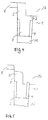
- Figure 1 shows a portion of an exemplary DRAM cell formed in a substrate 1 wherein the buried strap 5 is formed according to the method described in U.S. Pat. No. 5,360,758.
- a field-effect transistor denoted generally by numeral 10 has a source 11 and a drain 12 controlled by gate 13 as is conventional.
- a trench capacitor is formed as is known in the art by etching a deep trench 2 down into the substrate 1, forming an insulator along the trench surface (typically silicon dioxide and/or silicon nitride), filling it with doped polysilicon 15 up to a first level, then adding an isolating collar 4 of some convenient dielectric such as silicon dioxide or silicon nitride.
- the substrate surface is planarized by applying a filling material 9 followed by a layer of antireflective coating 6 so that the lithography can properly be performed.
- Typical filling materials comprise for example boronsilicate glass which is applied by chemical vapour deposition.
- an antireflective coating (ARC) which is applied in an appropriate thickness so as to additionally planarize the substrate surface, polymers, resist materials or other organic materials similar to resist materials can be used. Alternatively, such an antireflective material can also be used as the filling material itself.
- the trench 2 after lithographically patterning the resist layer 7.
- the isolation trench 17 for shallow trench isolation is etched as is shown in Figure 8.
- the etching depth amounts to the depth of the shallow trench isolation depth which is approximately 290 nm in the present case and the terminating point of this etching process is controlled by measuring the etching depth using an atomic force microscope.
- the resist 7 is stripped as is shown in Figure 9, and the process of defining the buried strap as well as the isolation trenches for shallow trench isolation is completed. Thereafter, an isolating material 14 will be filled into the isolation trench.
- planarizing material has to be filled into the recessed trench in order to planarize the surface of the substrate.
- this large thickness must be etched.
- any etching process will also attack the resist layer.
- a thick layer of resist material will be necessary, in order to make sure that a sufficient thickness of the photoresist material will remain after this etching step.
- a thick layer of photoresist material is disadvantageous when performing the lithography.
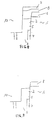
- FIG. 2 there is shown a portion of a DRAM cell formed in the semiconductor substrate 1 which is isolated by a thin silicon dioxide layer and a 150 nm silicon nitride layer 8.
- a deep trench 2 is filled with a center electrode material 15, which is usually doped polysilicon.
- the center electrode 15 is isolated from the substrate by a dielectric such as silicon dioxide, silicon nitride or a layered structure of silicon nitride/silicon dioxide or silicon dioxide/silicon nitride/silicon dioxide (20 in figure 1).
- an isolating collar 4 of a suitable dielectric such as silicon dioxide or silicon nitride is formed, and the conductive polysilicon 3 is filled into the center portion of the isolating collar 4.
- the strap material 5 is not recessed, i.e. the whole surface of the strap material remains at the same level as the isolating layer 8. Instead, the entire surface of the substrate including the deep trench 2 is coated with an antireflective coating 6 which normally is made of an organic material. Additionally, the resulting surface is covered by a resist layer 7 which is patterned by employing the methods commonly known in the art (photolithography).
- the shallow trench and the buried strap are etched to the final depth.
- the silicon in the trench and in the substrate are anisotropically etched.
- the remaining part of the silicon nitride layer 8 serves as an etching mask.
- the whole surface of the conductive material is etched down to a depth at which the part of the conductive material 5, which was covered with the resist material in Figure 3, now is below the lower edge of the substrate. Accordingly, a buried strap is formed.
- an isolating trench 17 is formed in the substrate 1.
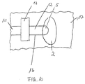
- Figure 10 is a schematic plan view of the DRAM cell which corresponds to the commonly known DRAM cell design.
- the active area 16 is adjacent to one side of the deep trench 2, and the remaining parts of the deep trench are surrounded by the isolation trench 17 which is filled with the isolating material 14. Thereby, an electric isolation of the DRAM cell is accomplished.
- the contour of the deep trench can be arbitrary and is not limited to be elliptic.
- the DRAM cell is finished by the conventional methods.
Landscapes
- Engineering & Computer Science (AREA)
- Manufacturing & Machinery (AREA)
- Semiconductor Memories (AREA)
- Semiconductor Integrated Circuits (AREA)
Priority Applications (1)
| Application Number | Priority Date | Filing Date | Title |
|---|---|---|---|
| EP00128017A EP1217657A1 (fr) | 2000-12-20 | 2000-12-20 | Procédé de fabriquer un ruban enterré dans une cellule DRAM |
Applications Claiming Priority (1)
| Application Number | Priority Date | Filing Date | Title |
|---|---|---|---|
| EP00128017A EP1217657A1 (fr) | 2000-12-20 | 2000-12-20 | Procédé de fabriquer un ruban enterré dans une cellule DRAM |
Publications (1)
| Publication Number | Publication Date |
|---|---|
| EP1217657A1 true EP1217657A1 (fr) | 2002-06-26 |
Family
ID=8170738
Family Applications (1)
| Application Number | Title | Priority Date | Filing Date |
|---|---|---|---|
| EP00128017A Withdrawn EP1217657A1 (fr) | 2000-12-20 | 2000-12-20 | Procédé de fabriquer un ruban enterré dans une cellule DRAM |
Country Status (1)
| Country | Link |
|---|---|
| EP (1) | EP1217657A1 (fr) |
Cited By (3)
| Publication number | Priority date | Publication date | Assignee | Title |
|---|---|---|---|---|
| CN101042997B (zh) * | 2006-03-21 | 2012-05-23 | 国际商业机器公司 | 利用前向馈送数据使沟槽凹陷至目标深度的方法和系统 |
| CN101958279B (zh) * | 2009-07-21 | 2013-01-16 | 中芯国际集成电路制造(上海)有限公司 | 提高沟槽宽度均匀性的方法 |
| CN102034735B (zh) * | 2009-09-27 | 2013-02-06 | 中芯国际集成电路制造(上海)有限公司 | 提高连接孔特征尺寸均匀性的方法 |
Citations (1)
| Publication number | Priority date | Publication date | Assignee | Title |
|---|---|---|---|---|
| US5389559A (en) * | 1993-12-02 | 1995-02-14 | International Business Machines Corporation | Method of forming integrated interconnect for very high density DRAMs |
-
2000
- 2000-12-20 EP EP00128017A patent/EP1217657A1/fr not_active Withdrawn
Patent Citations (1)
| Publication number | Priority date | Publication date | Assignee | Title |
|---|---|---|---|---|
| US5389559A (en) * | 1993-12-02 | 1995-02-14 | International Business Machines Corporation | Method of forming integrated interconnect for very high density DRAMs |
Non-Patent Citations (1)
| Title |
|---|
| "INTEGRATABLE RECESS 2 PROCESS FOR MEMORY STRUCTURES", IBM TECHNICAL DISCLOSURE BULLETIN,US,IBM CORP. NEW YORK, vol. 34, no. 4B, 1 September 1991 (1991-09-01), pages 291 - 292, XP000256682, ISSN: 0018-8689 * |
Cited By (3)
| Publication number | Priority date | Publication date | Assignee | Title |
|---|---|---|---|---|
| CN101042997B (zh) * | 2006-03-21 | 2012-05-23 | 国际商业机器公司 | 利用前向馈送数据使沟槽凹陷至目标深度的方法和系统 |
| CN101958279B (zh) * | 2009-07-21 | 2013-01-16 | 中芯国际集成电路制造(上海)有限公司 | 提高沟槽宽度均匀性的方法 |
| CN102034735B (zh) * | 2009-09-27 | 2013-02-06 | 中芯国际集成电路制造(上海)有限公司 | 提高连接孔特征尺寸均匀性的方法 |
Similar Documents
| Publication | Publication Date | Title |
|---|---|---|
| KR100413277B1 (ko) | 다이내믹 랜덤 엑세스 메모리 | |
| US5360758A (en) | Self-aligned buried strap for trench type DRAM cells | |
| US6426253B1 (en) | Method of forming a vertically oriented device in an integrated circuit | |
| US20050104110A1 (en) | Electronic devices including electrodes with insulating spacers thereon and related methods | |
| US5723381A (en) | Formation of self-aligned overlapping bitline contacts with sacrificial polysilicon fill-in stud | |
| EP0977256A2 (fr) | Procédé de fabriquer un condensateur ensillonné de type DRAM | |
| EP0682372A1 (fr) | Dispositif DRAM à condensateur supérieur et inférieur et méthode de fabrication | |
| CN107369686A (zh) | 半导体存储器元件及其制作方法 | |
| KR100509210B1 (ko) | Dram셀장치및그의제조방법 | |
| US6552381B2 (en) | Trench capacitors in SOI substrates | |
| US5843819A (en) | Semiconductor memory device with trench capacitor and method for the production thereof | |
| KR960003773B1 (ko) | 디램(DRAM) 셀(Cell) 제조방법 | |
| US6117726A (en) | Method of making a trench capacitor | |
| KR19980020386A (ko) | 반도체소자의 캐패시터 형성방법 | |
| JP3665614B2 (ja) | Dramセル装置の製法 | |
| US20040241939A1 (en) | METHOD OF FORMING A COLLAR USING SELECTIVE SiGe/AMORPHOUS Si ETCH | |
| US5701264A (en) | Dynamic random access memory cell having increased capacitance | |
| EP1217657A1 (fr) | Procédé de fabriquer un ruban enterré dans une cellule DRAM | |
| US6909136B2 (en) | Trench-capacitor DRAM cell having a folded gate conductor | |
| US6184078B1 (en) | Method for fabricating a capacitor for a dynamic random access memory cell | |
| US7078315B2 (en) | Method for eliminating inverse narrow width effects in the fabrication of DRAM device | |
| JP3685997B2 (ja) | 集積回路装置に適した凹部を備えた基板及びその製造方法 | |
| KR100305401B1 (ko) | 반도체소자의캐패시터형성방법 | |
| KR960011665B1 (ko) | 반도체 소자용 적층 캐패시터 형성방법 | |
| KR960003769B1 (ko) | 반도체메모리장치 및 그 제조방법 |
Legal Events
| Date | Code | Title | Description |
|---|---|---|---|
| PUAI | Public reference made under article 153(3) epc to a published international application that has entered the european phase |
Free format text: ORIGINAL CODE: 0009012 |
|
| AK | Designated contracting states |
Kind code of ref document: A1 Designated state(s): AT BE CH CY DE DK ES FI FR GB GR IE IT LI LU MC NL PT SE TR |
|
| AX | Request for extension of the european patent |
Free format text: AL;LT;LV;MK;RO;SI |
|
| AKX | Designation fees paid | ||
| REG | Reference to a national code |
Ref country code: DE Ref legal event code: 8566 |
|
| STAA | Information on the status of an ep patent application or granted ep patent |
Free format text: STATUS: THE APPLICATION IS DEEMED TO BE WITHDRAWN |
|
| 18D | Application deemed to be withdrawn |
Effective date: 20021228 |