EP1217725A1 - Monolithisch integrierte Spannungsschiebediode für Hyperfrequenzen, insbesondere für einen optoelektronischen Hyperfrequenzsender mit sehr hoher Bandbreite - Google Patents
Monolithisch integrierte Spannungsschiebediode für Hyperfrequenzen, insbesondere für einen optoelektronischen Hyperfrequenzsender mit sehr hoher Bandbreite Download PDFInfo
- Publication number
- EP1217725A1 EP1217725A1 EP01403225A EP01403225A EP1217725A1 EP 1217725 A1 EP1217725 A1 EP 1217725A1 EP 01403225 A EP01403225 A EP 01403225A EP 01403225 A EP01403225 A EP 01403225A EP 1217725 A1 EP1217725 A1 EP 1217725A1
- Authority
- EP
- European Patent Office
- Prior art keywords
- circuit
- diode
- offset
- downstream
- upstream
- Prior art date
- Legal status (The legal status is an assumption and is not a legal conclusion. Google has not performed a legal analysis and makes no representation as to the accuracy of the status listed.)
- Withdrawn
Links
- 230000005693 optoelectronics Effects 0.000 title description 4
- 238000011144 upstream manufacturing Methods 0.000 claims abstract description 22
- 238000005516 engineering process Methods 0.000 claims abstract description 9
- 230000010287 polarization Effects 0.000 claims description 15
- 238000001914 filtration Methods 0.000 claims description 6
- 230000000694 effects Effects 0.000 claims description 4
- 230000005669 field effect Effects 0.000 description 9
- 230000003321 amplification Effects 0.000 description 3
- 238000003199 nucleic acid amplification method Methods 0.000 description 3
- 239000013307 optical fiber Substances 0.000 description 3
- 230000005540 biological transmission Effects 0.000 description 2
- 238000010586 diagram Methods 0.000 description 2
- 239000000835 fiber Substances 0.000 description 2
- 229910052751 metal Inorganic materials 0.000 description 2
- 239000002184 metal Substances 0.000 description 2
- 238000005036 potential barrier Methods 0.000 description 2
- 239000004065 semiconductor Substances 0.000 description 2
- JBRZTFJDHDCESZ-UHFFFAOYSA-N AsGa Chemical compound [As]#[Ga] JBRZTFJDHDCESZ-UHFFFAOYSA-N 0.000 description 1
- 229910001218 Gallium arsenide Inorganic materials 0.000 description 1
- 239000008186 active pharmaceutical agent Substances 0.000 description 1
- 230000006978 adaptation Effects 0.000 description 1
- 230000015556 catabolic process Effects 0.000 description 1
- 238000010276 construction Methods 0.000 description 1
- 238000006731 degradation reaction Methods 0.000 description 1
- 235000021183 entrée Nutrition 0.000 description 1
- 229910052732 germanium Inorganic materials 0.000 description 1
- GNPVGFCGXDBREM-UHFFFAOYSA-N germanium atom Chemical compound [Ge] GNPVGFCGXDBREM-UHFFFAOYSA-N 0.000 description 1
- PCHJSUWPFVWCPO-UHFFFAOYSA-N gold Chemical compound [Au] PCHJSUWPFVWCPO-UHFFFAOYSA-N 0.000 description 1
- 239000010931 gold Substances 0.000 description 1
- 229910052737 gold Inorganic materials 0.000 description 1
- 230000001939 inductive effect Effects 0.000 description 1
- 238000004519 manufacturing process Methods 0.000 description 1
- 239000000463 material Substances 0.000 description 1
- 238000005272 metallurgy Methods 0.000 description 1
- 230000002787 reinforcement Effects 0.000 description 1
- 230000001502 supplementing effect Effects 0.000 description 1
Images




Classifications
-
- H—ELECTRICITY
- H03—ELECTRONIC CIRCUITRY
- H03F—AMPLIFIERS
- H03F3/00—Amplifiers with only discharge tubes or only semiconductor devices as amplifying elements
- H03F3/60—Amplifiers in which coupling networks have distributed constants, e.g. with waveguide resonators
- H03F3/605—Distributed amplifiers
- H03F3/607—Distributed amplifiers using FET's
-
- H—ELECTRICITY
- H03—ELECTRONIC CIRCUITRY
- H03F—AMPLIFIERS
- H03F1/00—Details of amplifiers with only discharge tubes, only semiconductor devices or only unspecified devices as amplifying elements
- H03F1/08—Modifications of amplifiers to reduce detrimental influences of internal impedances of amplifying elements
- H03F1/18—Modifications of amplifiers to reduce detrimental influences of internal impedances of amplifying elements by use of distributed coupling, i.e. distributed amplifiers
-
- H—ELECTRICITY
- H03—ELECTRONIC CIRCUITRY
- H03F—AMPLIFIERS
- H03F3/00—Amplifiers with only discharge tubes or only semiconductor devices as amplifying elements
- H03F3/04—Amplifiers with only discharge tubes or only semiconductor devices as amplifying elements with semiconductor devices only
- H03F3/08—Amplifiers with only discharge tubes or only semiconductor devices as amplifying elements with semiconductor devices only controlled by light
- H03F3/085—Amplifiers with only discharge tubes or only semiconductor devices as amplifying elements with semiconductor devices only controlled by light using opto-couplers between stages
Definitions
- the present invention relates to a shift diode in voltage realized in integrated microwave monolithic technology.
- Said offset diode is intended to ensure a voltage offset between two circuits including the downstream circuit consumes a relatively high bias current.
- the downstream circuit is an optoelectronic transmitter very broadband microwave, from a few Hz to several GHz, such as a laser diode.
- MMIC Monolithic Microwave Integrated Circuit
- a distributed amplifier (simple or transimpedance) has a plurality of amplifying cells basic, mounted between an input line and a line Release.
- Each basic amplifier cell has at least minus a field effect transistor, bipolar, or the like.
- each transistor is connected to the common drain line (outlet line) through its drain as well than to the common grid line (entry line) by its wire rack.
- the description will be limited to field effect transistors, but the skilled person knows that he can easily transpose the present invention to bipolar transistors or the like.
- the polarization filter circuits must let pass the DC bias voltages or currents and isolate the microwave power.
- the power supply terminal which receives the bias voltage from the drains of transistors is connected to the common drain line across bias resistance and decoupling ability in parallel connected to ground.
- the terminal which receives the bias voltage of transistor grids is connected to the grid line common across a bias resistor and a parallel decoupling capacity connected to ground.
- a link capacity is provided between the line of drains common, which forms the output of the distributed amplifier, and the anode of the laser diode.
- Such a link capacity isolates microwave power of continuous polarization.
- connection capacity by high-value capacity mounted outside the circuit cannot be considered here to increase the impedance of bonding capacity.
- a bonding capacity is placed between two non-zero voltage points, which prevents mounting of a capacity outside the integrated circuit (MMIC chip).
- the present invention provides a solution to this problem.
- It relates to an interface device between two circuits, the upstream circuit of which comprises an outlet and means for DC voltage polarization, and the downstream circuit includes input, uses DC bias voltage of higher value than that of the upstream circuit and consumes a relatively large bias current which is a function of the power delivered by the circuit downstream.
- the device interface includes a voltage offset diode mounted between the output of the upstream circuit and the input of the downstream circuit, the characteristic of the shift diode being chosen from so that the bias voltage of the upstream circuit either offset by an offset corresponding substantially to the difference between the bias voltages of the upstream circuits and downstream and whose value corresponds substantially to the threshold voltage of the shift diode, and the current of polarization of the downstream circuit being relatively large by relation to the threshold current of the shift diode.
- Such an offset diode eliminates the capacitance of connection between the upstream and downstream circuits, which makes said downstream circuit capable of operating over a very wide frequency band from a few Hz to several GHz.
- the bridge at diodes is used in a feedback loop in which passes a relatively weak current, substantially equal to the threshold current of the elementary diodes of the bridge at diodes.
- the shift diode comprises a plurality of transistors made in monolithic integrated technology microwave and mounted in parallel between the output of the upstream circuit and the input of the downstream circuit.
- each shift diode transistor includes a drain and a source connected to each other, each grid finger forming a diode effect contact.
- the downstream circuit includes a laser diode capable of emitting very broadband microwave signals.
- the upstream circuit includes a control circuit of the 50 ohm impedance laser diode and an amplifier distributed power acting as a low adapter impedance.
- the designs contain elements of a certain character. AT as such they can not only serve to do better understand the invention but also to contribute to the definition if necessary.
- the link uses direct amplitude modulation.
- the emitting head 4 comprises a laser diode 8 whose current is modulated by the radio frequency and microwave signal incident 12.
- the emitting head 4 comprises a device for polarization 10, if necessary a pre-amplification stage 14, and an impedance amplification and adaptation stage 16.
- the role of stage 16 is to adapt between the low impedance of the laser diode (around 10 ohms) and the classical impedance (50 ohms) of the input device (command) of the laser diode.
- a photodiode 20 picks up the signals transmitted by optical fiber 2.
- the receiving head 6 also includes an impedance matching stage 22, the if necessary a pre-amplification stage 24, and a device polarization of the photodiode 26.
- the output 28 of the receiving head can deliver a microwave signal at very broadband ranging from a few Hz to several GHz.
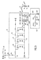
- stage 16 includes an amplifier distributed 18 says transimpedance playing the role of amplifier and low impedance adapter for the laser diode 8.
- the distributed amplifier 18 comprises a plurality of base amplifying cells AB, mounted between an input line (common line of drains LD in the case of field effect transistors mounted in common source) and an output line (LG common grid line).
- Each basic amplifier cell AB has at least one TEF field effect transistor mounted in common O source and connected to the common line of drains LD by its drain D as well than to the common grid line LG by its grid G.
- the BG supply terminal which receives the voltage of polarization VG of the gates of the transistors is connected to the common grid line LG through a resistor RG (from about 1 Kiloohms for example) and a capacity of decoupling CG in parallel connected to ground.
- Sons inductance IG1 and IG2 connect the power supply delivering the VG voltage at terminal BG.
- the common line of drains LD is polarized in voltage VD via a power supply filter circuit PD connected to the power supply terminal BD through inductors ID1, ID2 and ID3 and decoupling capacities CD1 and CD2 in parallel and connected to ground.
- the output S of the distributed amplifier 18 is connected to the anode 11 of the laser diode 8 through a ribbon or wire 17.
- the cathode 13 of the laser diode 8 is connected to ground.
- the laser diode 8 is biased at a bias voltage continues VL through an inductor 15, for example from around 15nH.
- the current of the laser diode 8 is of the order of 150 mA and the voltage of the laser diode 8 is around 1.4 volts.
- CL connection capacity is provided according to the prior art between the end of the common line of drains LD which forms the output S of the distributed amplifier and the anode 11 of the laser diode 8 (via ribbon 17).
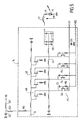
- the amplifier is shown distributed 18 described with reference to FIG. 2 in which has in particular replaced the CL capacitance by a diode DD offset according to the invention.
- the DD voltage offset diode is mounted between the end 32 of an inductor 34 forming the output S of the amplifier distributed 18 and the anode 11 of the laser diode 8 to through the wire or ribbon 17.
- the shift diode comprises a plurality of transistors made in monolithic microwave technology broadband and mounted in parallel between the outlet of the upstream circuit and the input of the downstream circuit.
- each transistor of the shift diode includes a drain and a source connected to each other, which forms an elementary diode DE.
- the DD shift diode includes for example two rows RA1 and RA2 of elementary diodes DE connected in parallel between the amplifier output distributed and the laser diode.
- the first row RA1 of elementary diodes DE comprises n individualized diodes in DE11 to DE1n, with for example n equal to 74 and the second row RA2 of elementary diodes includes n individualized diodes in DE21 to DE2n, with by example n equal to 74.
- the elementary diodes are arranged according to a arrangement in which the node 30-1 is connected in series to the output (here the end of inductance 34) of the amplifier distributed, and in parallel with the anode of the diode DE11 and at the anode of the diode DE21.
- node 30-2 is connected in series to node 30-1, and in parallel to the anode of the diode DE12 and the anode of diode DE22.
- the knot 30-n is connected in series to node 30-n-1, and in parallel with the anode of the diode DE1n and the anode of the diode DE2n.
- the cathodes of the elementary diodes DE are connected to the node 40 intended to be connected to the anode of the laser diode 8, via the ribbon 17 (if applicable).
- the 30-n node can advantageously play the power supply terminal which receives the bias voltage VD from the line of common drains LD through the filter circuit PD described with reference to Figure 2.
- the filtering circuit PD can also play the role of filtering the bias voltage VL of the laser diode 8, which eliminates the inductance 15 described with reference to Figure 2.
- CQ of the DD offset diode which gives the voltage continuous VL (in volts) across the offset diode DD as a function of the intensity ID (in amperes) passing through it.
- the DD offset diode is chosen so that the bias voltage VD of the common drain line LD either offset by an offset corresponding substantially to the difference between the bias voltage VD of the line of common drains LD and the bias voltage VL of the laser diode.
- the operating point PF of the diode of offset is chosen equal to 1.1 V with maximum intensity of 164 mA and the SL threshold of the diode offset is chosen equal to 0.925 V with an intensity 11 mA minimum.
- the threshold current (here 11 mA) of the offset diode is therefore relatively small compared to the current consumed by the downstream circuit (here 164 mA).
- the voltage offset is thus of the order of 1.1 V, which roughly corresponds to the operating point value PF of the DD offset diode.
- laser diode 8 Due to the removal of CL link capacity between the upstream 16 and downstream 8 circuits and its replacement by DD shift diode, laser diode 8 can work in a very wide frequency band ranging for example from a few Hz to several GHz.
- the PS circuit includes a plurality of transistors additional TS operating at saturable load.
- the SS sources of additional TS transistors are distributively connected to the common line of drains LD.
- the DS drains of the additional TS transistors receive series the bias voltage VD.
- the GS grids of the additional transistors receive in series a second VG2 gate bias voltage, the if necessary respectively through additional resistance RS.
- the voltage VG2 is connected to ground in parallel through a CSS decoupling capacity.
- each additional grid is linked to its source respective through additional capacity CS.
- the PS circuit remedies the drawbacks (energy loss, congestion) resulting from the filtering of the polarization across RG terminal resistors like that described with reference to Figure 2.
- the PS circuit remedies the disadvantages (degradations performance, impedance mismatch, resonance, dimensions, welds) resulting from the filtering of the polarization through inductive elements 15, ID1, ID2, ID3 like those described with reference to Figures 2 and / or 3.
- the shift diode DD comprises for example two rows RA1 and RA2 of n transistors. Each transistor forms a diode elementary DE by connecting its drain to its source.
- Each transistor includes a DG gate finger, individualized in DG11 to DG1n for the first row RA1 and in DG21 to DG2n for the second row RA2.
- Each gate finger DG of the diode DD is produced according to a contact called "Schottky” SK similar to the transistor grids field effect.
- a “Schottky” SK contact is a metal / semiconductor contact that results in a AC potential barrier. Such a “Schottky” contact presents a diode effect.
- the drains and the sources of the transistors of the shift diode are made according to a so-called "ohmic" contact OH which is a metal / semiconductor contact requiring a more complex metallurgy than that of the Schottky contact SK.
- ohmic contact generally involves materials of the Germanium, Gold, or Gallium Arsenide type, and results in the absence of a potential barrier. So it's a contact without diode effect with low resistance value.
- the intermediate zone AC between the ohmic contact and the Schottky contact is an active area.
- Each grid finger has an individual development of around 5 micrometers. So the shift diode has a total grid development of the order of 148 x 5 micrometers, or of the order of 740 micrometers.
- FIG 7 there is shown a mask which illustrates the construction of circuit 16 described with reference to Figure 3 and which includes a distributed amplifier 18 according to the invention and a DD shift diode.
Landscapes
- Engineering & Computer Science (AREA)
- Power Engineering (AREA)
- Amplifiers (AREA)
- Semiconductor Lasers (AREA)
- Microwave Amplifiers (AREA)
- Electrodes Of Semiconductors (AREA)
Applications Claiming Priority (2)
| Application Number | Priority Date | Filing Date | Title |
|---|---|---|---|
| FR0016937 | 2000-12-22 | ||
| FR0016937A FR2818829B1 (fr) | 2000-12-22 | 2000-12-22 | Diode de decalage en tension realisee en technologie integree monolithique hyperfrequence, notamment pour emetteur optoelectronique hyperfrequence a tres large bande |
Publications (1)
| Publication Number | Publication Date |
|---|---|
| EP1217725A1 true EP1217725A1 (de) | 2002-06-26 |
Family
ID=8858122
Family Applications (1)
| Application Number | Title | Priority Date | Filing Date |
|---|---|---|---|
| EP01403225A Withdrawn EP1217725A1 (de) | 2000-12-22 | 2001-12-12 | Monolithisch integrierte Spannungsschiebediode für Hyperfrequenzen, insbesondere für einen optoelektronischen Hyperfrequenzsender mit sehr hoher Bandbreite |
Country Status (4)
| Country | Link |
|---|---|
| US (1) | US20020139998A1 (de) |
| EP (1) | EP1217725A1 (de) |
| JP (1) | JP2002290169A (de) |
| FR (1) | FR2818829B1 (de) |
Cited By (1)
| Publication number | Priority date | Publication date | Assignee | Title |
|---|---|---|---|---|
| US6730945B2 (en) * | 2001-09-26 | 2004-05-04 | Mitsubishi Denki Kabushiki Kaisha | Semiconductor device |
Families Citing this family (3)
| Publication number | Priority date | Publication date | Assignee | Title |
|---|---|---|---|---|
| US6924697B2 (en) * | 2003-02-27 | 2005-08-02 | Freescale Semiconductor, Inc. | Semiconductor device and method thereof |
| JP2014096405A (ja) * | 2012-11-07 | 2014-05-22 | Sumitomo Electric Ind Ltd | 光送信回路 |
| CN104883800B (zh) * | 2015-06-15 | 2017-04-12 | 南京大学 | 一种GHz高速LED光通信驱动器 |
Citations (2)
| Publication number | Priority date | Publication date | Assignee | Title |
|---|---|---|---|---|
| EP0801467A1 (de) * | 1996-04-11 | 1997-10-15 | Dassault Electronique | Kettenverstärkender Adapter niedriger Impedanz für einen optoelektronischen Mikrowellensender mit sehr grosser Bandbreite |
| US5880640A (en) * | 1989-11-24 | 1999-03-09 | Dassault Electronique | Distributed amplifier for wide band hyperfrequency signals |
Family Cites Families (2)
| Publication number | Priority date | Publication date | Assignee | Title |
|---|---|---|---|---|
| FR2661790B1 (fr) * | 1990-05-03 | 1995-08-25 | France Etat | Dispositif d'amplification tres large bande continu-hyperfrequences, notamment realisable en circuit integre. |
| GB9920081D0 (en) * | 1999-08-24 | 1999-10-27 | Sgs Thomson Microelectronics | Current reference circuit |
-
2000
- 2000-12-22 FR FR0016937A patent/FR2818829B1/fr not_active Expired - Fee Related
-
2001
- 2001-12-05 US US10/001,978 patent/US20020139998A1/en not_active Abandoned
- 2001-12-06 JP JP2001372331A patent/JP2002290169A/ja not_active Withdrawn
- 2001-12-12 EP EP01403225A patent/EP1217725A1/de not_active Withdrawn
Patent Citations (3)
| Publication number | Priority date | Publication date | Assignee | Title |
|---|---|---|---|---|
| US5880640A (en) * | 1989-11-24 | 1999-03-09 | Dassault Electronique | Distributed amplifier for wide band hyperfrequency signals |
| EP0801467A1 (de) * | 1996-04-11 | 1997-10-15 | Dassault Electronique | Kettenverstärkender Adapter niedriger Impedanz für einen optoelektronischen Mikrowellensender mit sehr grosser Bandbreite |
| FR2747523A1 (fr) * | 1996-04-11 | 1997-10-17 | Dassault Electronique | Amplificateur distribue adaptateur basse impedance pour emetteur optoelectronique de signaux hyperfrequences a tres large bande |
Non-Patent Citations (1)
| Title |
|---|
| KIMURA S ET AL: "A 0-TO-40-GHZ DIRECT-COUPLED DISTRIBUTED BASEBAND AMPLIFIER IC WITHSCFL INTERFACE", IEEE MICROWAVE AND GUIDED WAVE LETTERS, IEEE INC, NEW YORK, US, vol. 6, no. 12, 1 December 1996 (1996-12-01), pages 444 - 446, XP000635323, ISSN: 1051-8207 * |
Cited By (1)
| Publication number | Priority date | Publication date | Assignee | Title |
|---|---|---|---|---|
| US6730945B2 (en) * | 2001-09-26 | 2004-05-04 | Mitsubishi Denki Kabushiki Kaisha | Semiconductor device |
Also Published As
| Publication number | Publication date |
|---|---|
| FR2818829B1 (fr) | 2003-03-28 |
| JP2002290169A (ja) | 2002-10-04 |
| US20020139998A1 (en) | 2002-10-03 |
| FR2818829A1 (fr) | 2002-06-28 |
Similar Documents
| Publication | Publication Date | Title |
|---|---|---|
| EP0586285B1 (de) | Optischer Sender-Empfänger für optische Datenübertragung und Schalteinrichtung | |
| EP0455570B1 (de) | Sehr breitbandige Verstärkungseinrichtung für Gleichstrom bis Mikrowellen, insbesondere geeignet für integrierte Schaltungen | |
| FR2842963A1 (fr) | Dispositif de charge active permettant de polariser un circuit amplificateur distribue tres large bande avec controle de gain | |
| EP1217725A1 (de) | Monolithisch integrierte Spannungsschiebediode für Hyperfrequenzen, insbesondere für einen optoelektronischen Hyperfrequenzsender mit sehr hoher Bandbreite | |
| Miyamoto et al. | 10-Gb/s strained MQW DFB-LD transmitter module and superlattice APD receiver module using GaAs MESFET IC's | |
| FR2855883A1 (fr) | Dispositif optoelectronique integre comportant un modulateur a electroabsorption et un element electronique de commande du modulateur | |
| EP0199332B1 (de) | Empfänger für optische Breitbandsignale | |
| EP0318379A1 (de) | Ultrahochfrequenzverstärker mit sehr breitem Durchlassbereich | |
| EP1771944B1 (de) | Klasse-ad-audioverstärker | |
| EP0726648B1 (de) | Abstimmschaltung für Empfangsgerät insbesondere Fernsehempfänger | |
| EP0368742B1 (de) | Digitalverstärker und diesen enthaltende integrierte Schaltung | |
| EP2182631A2 (de) | Mikrowellen-Breitband-Verstärkerzelle mit regelbarer Verstärkung und eine solche Zelle umfassender Verstärker | |
| EP0420106B1 (de) | Attenuatorschaltung mit einem Dual-Gate-Feldeffekttransistor | |
| EP0467450A1 (de) | Breitbandverstärker mit getrennten Ausgängen | |
| EP0801467B1 (de) | Kettenverstärkender Adapter niedriger Impedanz für einen optoelektronischen Mikrowellensender mit sehr grosser Bandbreite | |
| EP1017171B1 (de) | Phasensteuervorrichtung mit einer Vielzahl von Kettenverstärkerstrukturen mit schaltbaren aktiven Elementen zur Erstellung einer Übertragungsleitung mit programmierbarer Länge | |
| EP0986170A1 (de) | Schnittstelle zwischen einem breitbandigen optoelektronischen Sensor für Hyperfrequenzen und einer Last | |
| FR2759508A1 (fr) | Amplificateur distribue | |
| FR2747524A1 (fr) | Amplificateur adaptateur haute impedance pour recevoir des signaux hyperfrequences a tres large bande d'une source de courant capacitive a haute impedance telle qu'une photodiode | |
| WO2016097397A1 (fr) | Chaîne d'amplification du type dispositif de plot de gain améliorée | |
| WO1996008857A1 (en) | A low noise photon coupled circuit | |
| FR2955721A1 (fr) | Cellule amplificatrice hyperfrequence large bande a gain reglable faible cout et amplificateur distribue comportant une telle cellule | |
| FR2970388A1 (fr) | Amplificateur distribue large bande a gain controle automatiquement | |
| JP2923969B2 (ja) | 光スイッチ | |
| FR2955722A1 (fr) | Cellule amplificatrice hyperfrequence large bande a deux sorties a gain reglable de faible cout et repartiteur hyperfrequence comportant une telle cellule |
Legal Events
| Date | Code | Title | Description |
|---|---|---|---|
| PUAI | Public reference made under article 153(3) epc to a published international application that has entered the european phase |
Free format text: ORIGINAL CODE: 0009012 |
|
| AK | Designated contracting states |
Kind code of ref document: A1 Designated state(s): AT BE CH CY DE DK ES FI FR GB GR IE IT LI LU MC NL PT SE TR |
|
| AX | Request for extension of the european patent |
Free format text: AL;LT;LV;MK;RO;SI |
|
| 17P | Request for examination filed |
Effective date: 20020607 |
|
| D17P | Request for examination filed (deleted) | ||
| R17P | Request for examination filed (corrected) |
Effective date: 20021209 |
|
| AKX | Designation fees paid |
Designated state(s): AT BE CH CY DE DK ES FI FR GB GR IE IT LI LU MC NL PT SE TR |
|
| STAA | Information on the status of an ep patent application or granted ep patent |
Free format text: STATUS: THE APPLICATION IS DEEMED TO BE WITHDRAWN |
|
| 18D | Application deemed to be withdrawn |
Effective date: 20050701 |