EP1220077A2 - Dispositif de traitement de données et une carte mémoire qui utilise ce dispositif - Google Patents
Dispositif de traitement de données et une carte mémoire qui utilise ce dispositif Download PDFInfo
- Publication number
- EP1220077A2 EP1220077A2 EP01130510A EP01130510A EP1220077A2 EP 1220077 A2 EP1220077 A2 EP 1220077A2 EP 01130510 A EP01130510 A EP 01130510A EP 01130510 A EP01130510 A EP 01130510A EP 1220077 A2 EP1220077 A2 EP 1220077A2
- Authority
- EP
- European Patent Office
- Prior art keywords
- data
- control signal
- read
- write
- circuit
- Prior art date
- Legal status (The legal status is an assumption and is not a legal conclusion. Google has not performed a legal analysis and makes no representation as to the accuracy of the status listed.)
- Granted
Links
Images


Classifications
-
- G—PHYSICS
- G06—COMPUTING OR CALCULATING; COUNTING
- G06F—ELECTRIC DIGITAL DATA PROCESSING
- G06F12/00—Accessing, addressing or allocating within memory systems or architectures
- G06F12/14—Protection against unauthorised use of memory or access to memory
-
- G—PHYSICS
- G06—COMPUTING OR CALCULATING; COUNTING
- G06F—ELECTRIC DIGITAL DATA PROCESSING
- G06F13/00—Interconnection of, or transfer of information or other signals between, memories, input/output devices or central processing units
- G06F13/38—Information transfer, e.g. on bus
- G06F13/42—Bus transfer protocol, e.g. handshake; Synchronisation
- G06F13/4204—Bus transfer protocol, e.g. handshake; Synchronisation on a parallel bus
- G06F13/4234—Bus transfer protocol, e.g. handshake; Synchronisation on a parallel bus being a memory bus
- G06F13/4239—Bus transfer protocol, e.g. handshake; Synchronisation on a parallel bus being a memory bus with asynchronous protocol
Definitions
- a memory card which comprises: an operation processing unit having at least a read cycle period when the operation processing unit reads data from a device, and a write cycle period when the operation processing unit writes data in the device; a memory which performs data transmission/reception between the operation processing unit and the memory; a data bus connected to the operation processing unit and the memory; an input/output circuit connected to the data bus, the input/output circuit outputs external data onto the data bus and outputs data on the data bus to an external apparatus; and a dummy circuit connected to the data bus, the dummy circuit operates and consumes power in a time interval between the read cycle period and the write cycle period, between the write cycle period and the read cycle period, between two read cycle periods, or between two write cycle periods.
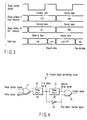
- An address to address a memory is transferred to the address bus 13 so that data stored in the memory 12 is read out by the CPU 11 accessing the memory 12 or so that data from the CPU 11 is written in the memory 12.
- Data to be transmitted/received between the CPU 11 and the memory 12 is transferred to the data bus 14.
- the data bus 14 has a large load capacity, and therefore a bus driving circuit is provided on each of the respective interfaces of the CPU 11 and the memory 12 in order to drive the large load capacity.
- the CPU 11 accesses the memory 12 and the read control signal is lowered to "0" level.
- data is read out from an address in the memory 12 corresponding to an address that is to be outputted from the CPU 11 and transferred on the address bus 13.
- the data read out from the memory 12 is outputted onto the data bus 14.
- the data outputted onto the data bus 14 is fetched by the CPU 11 at predetermined timing.
- a data processing apparatus provided with a random number data generating circuit is disclosed in Jpn. Pat. Appln. KOKAI Publication No. 8-249239. Random number data generated by the random number data generating circuit is transferred on a data bus and then fetched by a CPU, and the CPU performs operation processing using the random number data. In the data processing apparatus described in the publication, the random number data is, however, handled as part of normal data and thus transferred to the CPU through the data bus within the read cycle period. In other words, the data processing apparatus described in the publication is different from the data processing apparatus of the above-described embodiment in which pseudo-data is generated and outputted onto the data bus after the read cycle period or the write cycle period.
- the dummy circuit 23 operates and consumes power between two operation cycle periods forming any of combinations of the read cycle period and the write cycle period when original data is transmitted/received between the CPU 11 and the memory 12 through the data bus 14, and therefore, power consumption for transfer of two sets of original data including secret data to be transferred between the CPU 11 and the memory 12 is different from power consumption for operation of the dummy circuit 23 during the transfer.
- the above-mentioned memory 12 includes, for example, a ROM 12A, a RAM 12B and an EEPROM 12C as shown in FIG. 7.
Landscapes
- Engineering & Computer Science (AREA)
- Theoretical Computer Science (AREA)
- Physics & Mathematics (AREA)
- General Engineering & Computer Science (AREA)
- General Physics & Mathematics (AREA)
- Computer Security & Cryptography (AREA)
- Storage Device Security (AREA)
- Power Sources (AREA)
- Credit Cards Or The Like (AREA)
Applications Claiming Priority (2)
| Application Number | Priority Date | Filing Date | Title |
|---|---|---|---|
| JP2000400828 | 2000-12-28 | ||
| JP2000400828A JP3977592B2 (ja) | 2000-12-28 | 2000-12-28 | データ処理装置 |
Publications (3)
| Publication Number | Publication Date |
|---|---|
| EP1220077A2 true EP1220077A2 (fr) | 2002-07-03 |
| EP1220077A3 EP1220077A3 (fr) | 2003-07-02 |
| EP1220077B1 EP1220077B1 (fr) | 2007-05-09 |
Family
ID=18865346
Family Applications (1)
| Application Number | Title | Priority Date | Filing Date |
|---|---|---|---|
| EP01130510A Expired - Lifetime EP1220077B1 (fr) | 2000-12-28 | 2001-12-21 | Dispositif de traitement de données et une carte mémoire qui utilise ce dispositif |
Country Status (7)
| Country | Link |
|---|---|
| US (1) | US7533275B2 (fr) |
| EP (1) | EP1220077B1 (fr) |
| JP (1) | JP3977592B2 (fr) |
| KR (1) | KR100486808B1 (fr) |
| CN (1) | CN1230734C (fr) |
| DE (1) | DE60128323T2 (fr) |
| TW (1) | TW573274B (fr) |
Cited By (1)
| Publication number | Priority date | Publication date | Assignee | Title |
|---|---|---|---|---|
| EP1553500A1 (fr) * | 2004-01-07 | 2005-07-13 | Deutsche Thomson-Brandt Gmbh | Méthode et dispositif pour l'indication de données valides. |
Families Citing this family (12)
| Publication number | Priority date | Publication date | Assignee | Title |
|---|---|---|---|---|
| US8065532B2 (en) * | 2004-06-08 | 2011-11-22 | Hrl Laboratories, Llc | Cryptographic architecture with random instruction masking to thwart differential power analysis |
| JP4594665B2 (ja) * | 2004-07-09 | 2010-12-08 | 三菱電機株式会社 | 耐タンパ対策回路の評価装置、耐タンパ対策回路の評価方法、信号生成回路、信号生成方法、耐タンパ性評価装置及び耐タンパ性評価方法 |
| TWI263431B (en) * | 2004-09-22 | 2006-10-01 | Inst Information Industry | Data encryption system and method |
| KR101311963B1 (ko) * | 2007-08-06 | 2013-09-26 | 삼성전자주식회사 | 파워 어택으로부터 안전하게 데이터를 쓰고 읽을 수 있는반도체 메모리 장치 및 그 방법 |
| JP5359603B2 (ja) * | 2009-06-25 | 2013-12-04 | セイコーエプソン株式会社 | 集積回路システム、データ書き込み方法、データ読み出し方法 |
| JP5926655B2 (ja) * | 2012-08-30 | 2016-05-25 | ルネサスエレクトロニクス株式会社 | 中央処理装置および演算装置 |
| JP7177506B2 (ja) * | 2020-03-09 | 2022-11-24 | 京楽産業.株式会社 | 遊技機 |
| JP7177503B2 (ja) * | 2020-03-09 | 2022-11-24 | 京楽産業.株式会社 | 遊技機 |
| JP7177504B2 (ja) * | 2020-03-09 | 2022-11-24 | 京楽産業.株式会社 | 遊技機 |
| JP7177507B2 (ja) * | 2020-03-09 | 2022-11-24 | 京楽産業.株式会社 | 遊技機 |
| JP7177505B2 (ja) * | 2020-03-09 | 2022-11-24 | 京楽産業.株式会社 | 遊技機 |
| US20240388321A1 (en) * | 2023-05-18 | 2024-11-21 | Cisco Technology, Inc. | Delivering secured power to devices |
Family Cites Families (16)
| Publication number | Priority date | Publication date | Assignee | Title |
|---|---|---|---|---|
| NL8201847A (nl) * | 1982-05-06 | 1983-12-01 | Philips Nv | Inrichting voor het beschermen tegen onbevoegd uitlezen van in een geheugen te memoriseren programmawoorden. |
| FR2638869B1 (fr) * | 1988-11-10 | 1990-12-21 | Sgs Thomson Microelectronics | Dispositif de securite contre la detection non autorisee de donnees protegees |
| JPH02242327A (ja) * | 1989-03-15 | 1990-09-26 | Oki Electric Ind Co Ltd | 乱数発生装置 |
| FR2728369B1 (fr) | 1994-12-19 | 1997-01-31 | Sgs Thomson Microelectronics | Procede et dispositif pour accroitre la securite d'un circuit integre |
| JPH0926917A (ja) | 1995-07-11 | 1997-01-28 | Ekushingu:Kk | メモリ装置 |
| DE19642560A1 (de) | 1996-10-15 | 1998-04-16 | Siemens Ag | Elektronische Datenverarbeitungsschaltung |
| FR2776410B1 (fr) * | 1998-03-20 | 2002-11-15 | Gemplus Card Int | Dispositifs pour masquer les operations effectuees dans une carte a microprocesseur |
| ATE385089T1 (de) * | 1998-06-03 | 2008-02-15 | Cryptography Res Inc | Verwendung von unvorhersagbarer information zur leckminimierung von chipkarten und anderen kryptosystemen |
| DE19850721A1 (de) * | 1998-11-03 | 2000-05-18 | Koninkl Philips Electronics Nv | Datenträger mit Verschleierung des Stromverbrauchs |
| JP2000165375A (ja) * | 1998-11-30 | 2000-06-16 | Hitachi Ltd | 情報処理装置、icカード |
| FR2787900B1 (fr) * | 1998-12-28 | 2001-02-09 | Bull Cp8 | Circuit integre intelligent |
| JP2000285094A (ja) | 1999-03-31 | 2000-10-13 | Kawasaki Steel Corp | Eeprom内蔵マイクロコンピュータ |
| FR2793904B1 (fr) * | 1999-05-21 | 2001-07-27 | St Microelectronics Sa | Procede et dispositif de gestion d'un circuit electronique |
| US6419159B1 (en) * | 1999-06-14 | 2002-07-16 | Microsoft Corporation | Integrated circuit device with power analysis protection circuitry |
| FR2796738B1 (fr) * | 1999-07-22 | 2001-09-14 | Schlumberger Systems & Service | Micro-controleur securise contre les attaques en courant |
| FR2808360B1 (fr) * | 2000-04-28 | 2002-06-28 | Gemplus Card Int | Procede de contre mesure dans un microcircuit mettant en oeuvre le procede et carte a puce comportant ledit microcircuit |
-
2000
- 2000-12-28 JP JP2000400828A patent/JP3977592B2/ja not_active Expired - Fee Related
-
2001
- 2001-12-21 DE DE60128323T patent/DE60128323T2/de not_active Expired - Lifetime
- 2001-12-21 EP EP01130510A patent/EP1220077B1/fr not_active Expired - Lifetime
- 2001-12-21 TW TW90131799A patent/TW573274B/zh not_active IP Right Cessation
- 2001-12-27 US US10/026,813 patent/US7533275B2/en not_active Expired - Fee Related
- 2001-12-27 KR KR10-2001-0085955A patent/KR100486808B1/ko not_active Expired - Fee Related
- 2001-12-28 CN CNB011440899A patent/CN1230734C/zh not_active Expired - Fee Related
Cited By (1)
| Publication number | Priority date | Publication date | Assignee | Title |
|---|---|---|---|---|
| EP1553500A1 (fr) * | 2004-01-07 | 2005-07-13 | Deutsche Thomson-Brandt Gmbh | Méthode et dispositif pour l'indication de données valides. |
Also Published As
| Publication number | Publication date |
|---|---|
| CN1362662A (zh) | 2002-08-07 |
| US7533275B2 (en) | 2009-05-12 |
| JP2002202916A (ja) | 2002-07-19 |
| KR100486808B1 (ko) | 2005-05-03 |
| DE60128323T2 (de) | 2008-01-10 |
| DE60128323D1 (de) | 2007-06-21 |
| JP3977592B2 (ja) | 2007-09-19 |
| TW573274B (en) | 2004-01-21 |
| EP1220077A3 (fr) | 2003-07-02 |
| EP1220077B1 (fr) | 2007-05-09 |
| CN1230734C (zh) | 2005-12-07 |
| KR20020055422A (ko) | 2002-07-08 |
| US20020084333A1 (en) | 2002-07-04 |
Similar Documents
| Publication | Publication Date | Title |
|---|---|---|
| KR100365386B1 (ko) | 반도체메모리시스템과그동작방법및최대지연시간측정방법 | |
| US8195954B2 (en) | Smart cards including separate clocks for key processing and non-volatile memory interface communications and methods of operating the same | |
| EP0464433A2 (fr) | Microcontrôleur avec mémoire morte téléprogrammable et la méthode de programmation | |
| US6421291B1 (en) | Semiconductor memory device having high data input/output frequency and capable of efficiently testing circuit associated with data input/output | |
| CN110892483B (zh) | 采用有限数量的测试引脚测试存储器件的方法以及利用该方法的存储器件 | |
| EP1220077A2 (fr) | Dispositif de traitement de données et une carte mémoire qui utilise ce dispositif | |
| US5884074A (en) | Microcomputer utilizing flash memory for data storage | |
| US20070050167A1 (en) | Techniques for generating test patterns in high speed memory devices | |
| US6158036A (en) | Merged memory and logic (MML) integrated circuits including built-in test circuits and methods | |
| US6892269B2 (en) | Nonvolatile memory device with double serial/parallel communication interface | |
| US7782682B2 (en) | Semiconductor device with circuitry for efficient information exchange | |
| US6543019B2 (en) | Method for built-in self test of an electronic circuit | |
| WO2008024336A2 (fr) | Procédé et système de masque de données d'écriture | |
| KR100564033B1 (ko) | 단일 버퍼 선택 입력 단자를 가지는 반도체 메모리 및반도체 메모리 테스트 방법 | |
| US20070038795A1 (en) | Asynchronous bus interface and processing method thereof | |
| KR100327637B1 (ko) | 버스트모드형반도체메모리장치 | |
| US6611929B1 (en) | Test circuit for memory | |
| US6226211B1 (en) | Merged memory-logic semiconductor device having a built-in self test circuit | |
| JP2001243797A (ja) | 半導体装置及びその試験方法 | |
| US5818794A (en) | Internally controlled signal system for controlling the operation of a device | |
| US6088271A (en) | Method and apparatus for transferring signal to circuit without waveform distortion | |
| JP2877505B2 (ja) | Lsi実装ボード及びデータ処理装置 | |
| US6038617A (en) | Auto configuration of a serial ROM by sensing an output of the serial ROM after transmission of a read instruction and an x-bit address to it's input | |
| US5943492A (en) | Apparatus and method for generating external interface signals in a microprocessor | |
| JP2002093198A (ja) | 半導体装置 |
Legal Events
| Date | Code | Title | Description |
|---|---|---|---|
| PUAI | Public reference made under article 153(3) epc to a published international application that has entered the european phase |
Free format text: ORIGINAL CODE: 0009012 |
|
| 17P | Request for examination filed |
Effective date: 20011221 |
|
| AK | Designated contracting states |
Kind code of ref document: A2 Designated state(s): AT BE CH CY DE DK ES FI FR GB GR IE IT LI LU MC NL PT SE TR |
|
| AX | Request for extension of the european patent |
Free format text: AL;LT;LV;MK;RO;SI |
|
| RIC1 | Information provided on ipc code assigned before grant |
Ipc: 7G 07F 7/10 B Ipc: 7G 06F 1/00 A |
|
| PUAL | Search report despatched |
Free format text: ORIGINAL CODE: 0009013 |
|
| AK | Designated contracting states |
Designated state(s): AT BE CH CY DE DK ES FI FR GB GR IE IT LI LU MC NL PT SE TR |
|
| AX | Request for extension of the european patent |
Extension state: AL LT LV MK RO SI |
|
| AKX | Designation fees paid |
Designated state(s): DE FR GB |
|
| 17Q | First examination report despatched |
Effective date: 20040304 |
|
| GRAP | Despatch of communication of intention to grant a patent |
Free format text: ORIGINAL CODE: EPIDOSNIGR1 |
|
| RIC1 | Information provided on ipc code assigned before grant |
Ipc: G06F 21/00 20060101AFI20060616BHEP Ipc: G07F 7/10 20060101ALI20060616BHEP |
|
| GRAS | Grant fee paid |
Free format text: ORIGINAL CODE: EPIDOSNIGR3 |
|
| GRAA | (expected) grant |
Free format text: ORIGINAL CODE: 0009210 |
|
| AK | Designated contracting states |
Kind code of ref document: B1 Designated state(s): DE FR GB |
|
| REG | Reference to a national code |
Ref country code: GB Ref legal event code: FG4D |
|
| REF | Corresponds to: |
Ref document number: 60128323 Country of ref document: DE Date of ref document: 20070621 Kind code of ref document: P |
|
| ET | Fr: translation filed | ||
| PLBE | No opposition filed within time limit |
Free format text: ORIGINAL CODE: 0009261 |
|
| STAA | Information on the status of an ep patent application or granted ep patent |
Free format text: STATUS: NO OPPOSITION FILED WITHIN TIME LIMIT |
|
| 26N | No opposition filed |
Effective date: 20080212 |
|
| REG | Reference to a national code |
Ref country code: FR Ref legal event code: PLFP Year of fee payment: 15 |
|
| PGFP | Annual fee paid to national office [announced via postgrant information from national office to epo] |
Ref country code: GB Payment date: 20151216 Year of fee payment: 15 Ref country code: DE Payment date: 20151215 Year of fee payment: 15 |
|
| PGFP | Annual fee paid to national office [announced via postgrant information from national office to epo] |
Ref country code: FR Payment date: 20151110 Year of fee payment: 15 |
|
| REG | Reference to a national code |
Ref country code: DE Ref legal event code: R119 Ref document number: 60128323 Country of ref document: DE |
|
| GBPC | Gb: european patent ceased through non-payment of renewal fee |
Effective date: 20161221 |
|
| REG | Reference to a national code |
Ref country code: FR Ref legal event code: ST Effective date: 20170831 |
|
| PG25 | Lapsed in a contracting state [announced via postgrant information from national office to epo] |
Ref country code: FR Free format text: LAPSE BECAUSE OF NON-PAYMENT OF DUE FEES Effective date: 20170102 |
|
| PG25 | Lapsed in a contracting state [announced via postgrant information from national office to epo] |
Ref country code: DE Free format text: LAPSE BECAUSE OF NON-PAYMENT OF DUE FEES Effective date: 20170701 Ref country code: GB Free format text: LAPSE BECAUSE OF NON-PAYMENT OF DUE FEES Effective date: 20161221 |