EP1220444A1 - Montage amplificateur de sortie différentiel - Google Patents
Montage amplificateur de sortie différentiel Download PDFInfo
- Publication number
- EP1220444A1 EP1220444A1 EP00403709A EP00403709A EP1220444A1 EP 1220444 A1 EP1220444 A1 EP 1220444A1 EP 00403709 A EP00403709 A EP 00403709A EP 00403709 A EP00403709 A EP 00403709A EP 1220444 A1 EP1220444 A1 EP 1220444A1
- Authority
- EP
- European Patent Office
- Prior art keywords
- arrangement
- amplifier
- resistor
- input terminal
- doa
- Prior art date
- Legal status (The legal status is an assumption and is not a legal conclusion. Google has not performed a legal analysis and makes no representation as to the accuracy of the status listed.)
- Withdrawn
Links
- 230000008878 coupling Effects 0.000 claims description 6
- 238000010168 coupling process Methods 0.000 claims description 6
- 238000005859 coupling reaction Methods 0.000 claims description 6
- 101100396986 Saccharomyces cerevisiae (strain ATCC 204508 / S288c) INN1 gene Proteins 0.000 abstract description 6
- 101150071403 INP1 gene Proteins 0.000 abstract description 2
- 101150016601 INP2 gene Proteins 0.000 abstract description 2
- 230000005540 biological transmission Effects 0.000 description 3
- 238000006880 cross-coupling reaction Methods 0.000 description 3
- 101000730648 Homo sapiens Phospholipase A-2-activating protein Proteins 0.000 description 1
- 102100032572 Phospholipase A-2-activating protein Human genes 0.000 description 1
- 230000000694 effects Effects 0.000 description 1
- 238000000034 method Methods 0.000 description 1
Images
Classifications
-
- H—ELECTRICITY
- H03—ELECTRONIC CIRCUITRY
- H03F—AMPLIFIERS
- H03F3/00—Amplifiers with only discharge tubes or only semiconductor devices as amplifying elements
- H03F3/34—DC amplifiers in which all stages are DC-coupled
- H03F3/343—DC amplifiers in which all stages are DC-coupled with semiconductor devices only
- H03F3/347—DC amplifiers in which all stages are DC-coupled with semiconductor devices only in integrated circuits
Definitions
- the present invention relates to a differential output amplifier arrangement as defined in the non-characteristic part of claim 1.
- differential output amplifier arrangement is already known in the art, e.g. from the European Patent Application EP 0 901 221 from applicant Alcatel, entitled 'Differential Output Amplifier Arrangement and Method for Tuning the Output Impedance of a Differential Output Amplifier'.
- the differential output amplifier arrangement disclosed therein is active back terminated.
- the signal source is coupled to the positive input terminals of the operational amplifiers, whereas a resistor interconnects the negative input terminals of the operational amplifiers. This configuration at the entrance does not allow to realise the biasing and gain control for the amplifier arrangement with a minimum amount of components.
- An object of the present invention is to provide a differential output amplifier arrangement similar to the known one, but whose biasing and gain control can be realised with a minimum amount of components.
- a signal source can be directly coupled to the input terminals of the amplifier arrangement according to the present invention.
- This signal source could not be directly coupled to the input terminals of the prior art amplifier arrangement because the biasing there required two resistors to be inserted between the signal source and the input terminals of the amplifier arrangement.
- These biasing resistors inherently form part of the amplifier arrangement according to the present invention wherein no longer a resistor interconnecting the negative input terminals of the two operational amplifiers is needed, which was the case in the prior art solution.
- the term 'coupled' should not be interpreted as being limitative to direct connections only.
- the scope of the expression 'a device A coupled to a device B' should not be limited to devices or systems wherein an output of device A is directly connected to an input of device B. It means that there exists a path between an output of A and an input of B which may be a path including other devices or means.
- the biasing resistors preferably have substantial equal resistance values.
- the amplifier arrangement according to the present invention becomes a stable system from point of view of system theory, which implies that the arrangement will not oscillate.
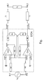
- the differential output amplifier arrangement DOA represented in the drawing has two arrangement input terminals denoted by IN1 and IN2, and two arrangement output terminals denoted by ZOUT1 and ZOUT2. To the arrangement input terminals IN1 and IN2 terminals of a differential input signal source are coupled. The arrangement output terminals ZOUT1 and ZOUT2 are coupled to transmission lines T1 and T2.
- the differential output amplifier arrangement DOA further includes two operational amplifiers, OA1 and OA2, having respective non-inverting input terminals INP1 and INP2, respective inverting input terminals INN1 and INN2, and having respective output terminals OUT1 and OUT2.
- the output terminal OUT1 of the first operational amplifier OA1 is coupled to the first arrangement output terminal ZOUT1 via a first resistor R1, and feedback coupled to the inverting input terminal INN1 of this first operational amplifier OA1 via a second resistor R2.
- the output terminal OUT2 of the second operational amplifier OA2 is coupled to the second arrangement output terminal ZOUT2 via a third resistor R3, and feedback coupled to the inverting input terminal INN2 of this second operational amplifier OA2 via a fourth resistor R4.
- the differential output amplifier arrangement DOA1 contains two additional resistors, a fifth resistor R5 cross-coupling the first arrangement output terminal ZOUT1 to the inverting input terminal INN2 of the second operational amplifier OA2, and a sixth resistor R6 cross-coupling the second arrangement output terminal ZOUT2 to the inverting input terminal INN1 of the first operational amplifier OA1.
- These two resistors, R5 and R6, together with the first resistor R1 and the third resistor R3 constitute an active back termination that allows to tune the output impedance of the arrangement DOA to a desired value.
- the output impedance of the arrangement DOA matches a load impedance which is denoted by RL in the drawing, and which in the drawing is coupled to the transmission lines T1 and T2 via terminals RL1 and RL2.
- the characteristic impedance of the transmission lines T1 and T2 is supposed to be equal to RL/2 for matching purposes.
- the voltage drop over the first resistor R1 and third resistor R3 of this active back termination allow the arrangement DOA to deliver an output signal having a given power with reduced supply voltage for the operational amplifiers OA1 and OA2, and/or with an increased dynamic range for both operational amplifiers OA1 and OA2.
- the differential output amplifier arrangement DOA furthermore contains a seventh resistor R7 coupled between the first arrangement input terminal IN1 and the inverting input terminal INN1 of the first operational amplifier OA1, and an eighth resistor R8, coupled between the second arrangement input terminal IN2 and the inverting input terminal INN2 of the second operational amplifier OA2. Between the first input terminal IN1 and the second input terminal IN2 of the arrangement DOA, the differential input signal Vs is applied.
- A R7.R2 - R7.R1 + R7.R5 + 2.R2.R5 2.R7.R1.R5 + RL.R7.R5 + RL.R7.R1- RL.R7.R2 .RL
- the resistance values R1, R2, R5 and R7 on the basis of the formula's (1) and (2) can be chosen so that the desired gain and arrangement output impedance are realised.
- the resistors R7 and R8 that allow to tune the gain A of the differential output amplifier arrangement DOA realise the input DC biasing.
- Such biasing is not realised by the arrangement known from EP 0 901 221, and has to be provided for there by two additional resistors coupling the input terminals of the operational amplifiers to the ground or a reference level.
- the biasing and gain control is thus more efficiently realised in the arrangement according to the present invention, since less components are required in the end.
- An embodiment of the amplifier arrangement DOA can be used for instance in an ADSL (Asynchronous Digital Subscriber Line) line driver.
- the characteristic impedance in such a line driver is transformed by a hybrid into a value of 12.5 Ohm observed at the output of the operational amplifiers OA1 and OA2.
- the load resistance RL has an equivalent resistance value of 25 Ohm for matching purposes.
- the desired gain A is set by surrounding system considerations, that fall beyond the scope of this patent application.
- the operational amplifiers and resistance values may be chosen as follows:
Landscapes
- Engineering & Computer Science (AREA)
- Microelectronics & Electronic Packaging (AREA)
- Power Engineering (AREA)
- Amplifiers (AREA)
Priority Applications (3)
| Application Number | Priority Date | Filing Date | Title |
|---|---|---|---|
| EP00403709A EP1220444A1 (fr) | 2000-12-28 | 2000-12-28 | Montage amplificateur de sortie différentiel |
| JP2001388784A JP2002223134A (ja) | 2000-12-28 | 2001-12-21 | 差動出力増幅器装置 |
| US10/026,434 US20020118063A1 (en) | 2000-12-28 | 2001-12-27 | Differential output amplifier arrangement |
Applications Claiming Priority (1)
| Application Number | Priority Date | Filing Date | Title |
|---|---|---|---|
| EP00403709A EP1220444A1 (fr) | 2000-12-28 | 2000-12-28 | Montage amplificateur de sortie différentiel |
Publications (1)
| Publication Number | Publication Date |
|---|---|
| EP1220444A1 true EP1220444A1 (fr) | 2002-07-03 |
Family
ID=8174016
Family Applications (1)
| Application Number | Title | Priority Date | Filing Date |
|---|---|---|---|
| EP00403709A Withdrawn EP1220444A1 (fr) | 2000-12-28 | 2000-12-28 | Montage amplificateur de sortie différentiel |
Country Status (3)
| Country | Link |
|---|---|
| US (1) | US20020118063A1 (fr) |
| EP (1) | EP1220444A1 (fr) |
| JP (1) | JP2002223134A (fr) |
Cited By (1)
| Publication number | Priority date | Publication date | Assignee | Title |
|---|---|---|---|---|
| US7330703B2 (en) | 2003-06-26 | 2008-02-12 | Broadcom Corporation | Transceiver for bidirectional frequency division multiplexed transmission |
Families Citing this family (2)
| Publication number | Priority date | Publication date | Assignee | Title |
|---|---|---|---|---|
| TWI346446B (en) * | 2008-04-21 | 2011-08-01 | Advanced Analog Technology Inc | Multi-input operational amplifier and method for reducing input offset thereof |
| WO2012032736A1 (fr) * | 2010-09-10 | 2012-03-15 | 旭化成エレクトロニクス株式会社 | Circuit d'amplification |
Citations (3)
| Publication number | Priority date | Publication date | Assignee | Title |
|---|---|---|---|---|
| EP0809353A2 (fr) * | 1996-05-20 | 1997-11-26 | Kabushiki Kaisha Toshiba | Amplificateur pour supprimer le bruit entre circuits |
| EP0901221A1 (fr) * | 1997-09-05 | 1999-03-10 | Alcatel | Dispositif amplificateur de sortie différentiel et méthode d'accord de l'impédance de sortie d'un tel amplificateur |
| FR2778513A1 (fr) * | 1998-05-06 | 1999-11-12 | Matra Nortel Communications | Circuit de traitement de signal analogique |
-
2000
- 2000-12-28 EP EP00403709A patent/EP1220444A1/fr not_active Withdrawn
-
2001
- 2001-12-21 JP JP2001388784A patent/JP2002223134A/ja not_active Withdrawn
- 2001-12-27 US US10/026,434 patent/US20020118063A1/en not_active Abandoned
Patent Citations (3)
| Publication number | Priority date | Publication date | Assignee | Title |
|---|---|---|---|---|
| EP0809353A2 (fr) * | 1996-05-20 | 1997-11-26 | Kabushiki Kaisha Toshiba | Amplificateur pour supprimer le bruit entre circuits |
| EP0901221A1 (fr) * | 1997-09-05 | 1999-03-10 | Alcatel | Dispositif amplificateur de sortie différentiel et méthode d'accord de l'impédance de sortie d'un tel amplificateur |
| FR2778513A1 (fr) * | 1998-05-06 | 1999-11-12 | Matra Nortel Communications | Circuit de traitement de signal analogique |
Cited By (3)
| Publication number | Priority date | Publication date | Assignee | Title |
|---|---|---|---|---|
| US7330703B2 (en) | 2003-06-26 | 2008-02-12 | Broadcom Corporation | Transceiver for bidirectional frequency division multiplexed transmission |
| US7450715B2 (en) | 2003-06-26 | 2008-11-11 | Broadcom Corporation | Transceiver for bidirectional frequency division multiplexed transmission |
| US7940707B2 (en) | 2003-06-26 | 2011-05-10 | Broadcom Corporation | Transceiver for bidirectional frequency division multiplexed transmission |
Also Published As
| Publication number | Publication date |
|---|---|
| US20020118063A1 (en) | 2002-08-29 |
| JP2002223134A (ja) | 2002-08-09 |
Similar Documents
| Publication | Publication Date | Title |
|---|---|---|
| US5023951A (en) | Optical receivers | |
| EP0901221B1 (fr) | Dispositif amplificateur de sortie différentiel et méthode d'accord de l'impédance de sortie d'un tel amplificateur | |
| US4472608A (en) | Subscriber line interface circuit | |
| WO2000052820A1 (fr) | Amplificateurs d'adaptation d'impedance a produit gain-bande ameliore | |
| US5013903A (en) | Lightwave receiver having differential input | |
| US4803721A (en) | DC control circuit | |
| US6028482A (en) | Wide dynamic range transimpedance amplifier circuit | |
| JPS58501530A (ja) | 加入者ル−プインタフエ−ス回路用平衡電流倍率器回路 | |
| US4453038A (en) | Circuit arrangement for producing control means from line current | |
| EP1220444A1 (fr) | Montage amplificateur de sortie différentiel | |
| KR970003720B1 (ko) | 전기신호 증폭기 장치 | |
| KR930002588B1 (ko) | 제한된 전지전압에서 왜곡이 없는 음성신호의 전송이 가능하도록 전화선에 전력을 공급하는 방법 및 장치 | |
| GB2295289A (en) | Wideband constant impedance amplifiers | |
| US4718083A (en) | Differential receive booster amplifier for telephone instruments | |
| EP0493519B1 (fr) | Amplificateur de sortie | |
| JPH08250942A (ja) | トランスインピーダンス増幅器回路 | |
| JPS6135733B2 (fr) | ||
| CA2144420C (fr) | Circuit pour amplificateur a sorties integrees | |
| EP0250763B1 (fr) | Amplificateur sommateur de type differentiel pour des tensions d'entrée à mode commun élevé | |
| US4554415A (en) | Bilateral amplifier | |
| US3935480A (en) | Broad band directional signal generator | |
| JP3875726B2 (ja) | フィルタ及び発振器用の相補トランスコンダクタを具えている電子回路 | |
| US4758822A (en) | Bidirectional amplifier | |
| EP1049249A1 (fr) | Amplificateur à gain variable | |
| GB2066026A (en) | Active speech network for a telephone set |
Legal Events
| Date | Code | Title | Description |
|---|---|---|---|
| PUAI | Public reference made under article 153(3) epc to a published international application that has entered the european phase |
Free format text: ORIGINAL CODE: 0009012 |
|
| AK | Designated contracting states |
Kind code of ref document: A1 Designated state(s): AT BE CH CY DE DK ES FI FR GB GR IE IT LI LU MC NL PT SE TR |
|
| AX | Request for extension of the european patent |
Free format text: AL;LT;LV;MK;RO;SI |
|
| STAA | Information on the status of an ep patent application or granted ep patent |
Free format text: STATUS: THE APPLICATION HAS BEEN WITHDRAWN |
|
| 18W | Application withdrawn |
Withdrawal date: 20021126 |