EP1220449A2 - Verstärker - Google Patents
Verstärker Download PDFInfo
- Publication number
- EP1220449A2 EP1220449A2 EP01310458A EP01310458A EP1220449A2 EP 1220449 A2 EP1220449 A2 EP 1220449A2 EP 01310458 A EP01310458 A EP 01310458A EP 01310458 A EP01310458 A EP 01310458A EP 1220449 A2 EP1220449 A2 EP 1220449A2
- Authority
- EP
- European Patent Office
- Prior art keywords
- switches
- differential input
- amplifier
- input transistors
- signal
- Prior art date
- Legal status (The legal status is an assumption and is not a legal conclusion. Google has not performed a legal analysis and makes no representation as to the accuracy of the status listed.)
- Withdrawn
Links
Images


Classifications
-
- H—ELECTRICITY
- H03—ELECTRONIC CIRCUITRY
- H03K—PULSE TECHNIQUE
- H03K5/00—Manipulating of pulses not covered by one of the other main groups of this subclass
- H03K5/01—Shaping pulses
- H03K5/02—Shaping pulses by amplifying
-
- H—ELECTRICITY
- H03—ELECTRONIC CIRCUITRY
- H03K—PULSE TECHNIQUE
- H03K5/00—Manipulating of pulses not covered by one of the other main groups of this subclass
- H03K5/22—Circuits having more than one input and one output for comparing pulses or pulse trains with each other according to input signal characteristics, e.g. slope, integral
- H03K5/24—Circuits having more than one input and one output for comparing pulses or pulse trains with each other according to input signal characteristics, e.g. slope, integral the characteristic being amplitude
- H03K5/2472—Circuits having more than one input and one output for comparing pulses or pulse trains with each other according to input signal characteristics, e.g. slope, integral the characteristic being amplitude using field effect transistors
- H03K5/249—Circuits having more than one input and one output for comparing pulses or pulse trains with each other according to input signal characteristics, e.g. slope, integral the characteristic being amplitude using field effect transistors using clock signals
-
- H—ELECTRICITY
- H03—ELECTRONIC CIRCUITRY
- H03K—PULSE TECHNIQUE
- H03K5/00—Manipulating of pulses not covered by one of the other main groups of this subclass
- H03K5/22—Circuits having more than one input and one output for comparing pulses or pulse trains with each other according to input signal characteristics, e.g. slope, integral
- H03K5/24—Circuits having more than one input and one output for comparing pulses or pulse trains with each other according to input signal characteristics, e.g. slope, integral the characteristic being amplitude
- H03K5/2472—Circuits having more than one input and one output for comparing pulses or pulse trains with each other according to input signal characteristics, e.g. slope, integral the characteristic being amplitude using field effect transistors
- H03K5/2481—Circuits having more than one input and one output for comparing pulses or pulse trains with each other according to input signal characteristics, e.g. slope, integral the characteristic being amplitude using field effect transistors with at least one differential stage
-
- H—ELECTRICITY
- H04—ELECTRIC COMMUNICATION TECHNIQUE
- H04N—PICTORIAL COMMUNICATION, e.g. TELEVISION
- H04N23/00—Cameras or camera modules comprising electronic image sensors; Control thereof
- H04N23/60—Control of cameras or camera modules
- H04N23/65—Control of camera operation in relation to power supply
-
- H—ELECTRICITY
- H04—ELECTRIC COMMUNICATION TECHNIQUE
- H04N—PICTORIAL COMMUNICATION, e.g. TELEVISION
- H04N23/00—Cameras or camera modules comprising electronic image sensors; Control thereof
- H04N23/60—Control of cameras or camera modules
- H04N23/66—Remote control of cameras or camera parts, e.g. by remote control devices
- H04N23/661—Transmitting camera control signals through networks, e.g. control via the Internet
-
- H—ELECTRICITY
- H04—ELECTRIC COMMUNICATION TECHNIQUE
- H04N—PICTORIAL COMMUNICATION, e.g. TELEVISION
- H04N23/00—Cameras or camera modules comprising electronic image sensors; Control thereof
- H04N23/60—Control of cameras or camera modules
- H04N23/67—Focus control based on electronic image sensor signals
- H04N23/673—Focus control based on electronic image sensor signals based on contrast or high frequency components of image signals, e.g. hill climbing method
-
- H—ELECTRICITY
- H04—ELECTRIC COMMUNICATION TECHNIQUE
- H04N—PICTORIAL COMMUNICATION, e.g. TELEVISION
- H04N25/00—Circuitry of solid-state image sensors [SSIS]; Control thereof
- H04N25/60—Noise processing, e.g. detecting, correcting, reducing or removing noise
- H04N25/618—Noise processing, e.g. detecting, correcting, reducing or removing noise for random or high-frequency noise
Definitions
- the present invention relates to an amplifier and an image pickup device, and more particularly to an amplifier and an image pickup device in which a power consumed by the amplifier and an electric characteristic hardly change while a 1/f noise generated from a transistor that constitutes a circuit is reduced.
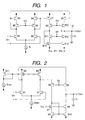
- Fig. 1 shows a conventional differential amplifier using a MOS transistor.
- Differential input signal voltages applied to the inverse and non-inverse input terminals which are connected to the respective gate terminals of MOS transistors M1 and M2, by a differential input stage that is connected with the respective source terminals of the MOS transistors M1 and M2 are converted into signal currents, and the signal currents are transmitted by a current mirror circuit composed of MOS transistors M3 to M10 and are then added to a current that is inverted by a current mirror circuit composed of MOS transistors M11 to M14 at a node A, and then converted into a signal voltage by an impedance and a load resistor accompanied by the node A and finally outputted from an output terminal 10.
- the largest sources that generate random noises that appears in the output terminal 10 of the differential amplifier are the MOS transistors M1 and M2 that appear to be input transistors from the view point of transfer function up to the output terminal 10, and the MOS transistors M1 and M2 generally are a main generation sources of a noise that has a larger spectrum with respect to a lower frequency called "1/f noise" that is classified as one kind of the random noise.
- the electric characteristic of the differential amplifier largely depends on the dimensions and characteristics of the input transistors M1 and M2, the electric characteristics are not normally designed in view of the 1/f noise alone, but determined in accordance with the their trade-off. Therefore, there are many cases in which it is difficult to change the gate dimensions of the input transistor to reduce the 1/f noises, after the differential amplifier that satisfies the required specification has been briefly designed.
- Fig. 2 shows a conventional example (of structure) different from that of Fig. 1, a type called “folded cascode", which is identical with that of Fig. 1 except that MOS transistors M3 and M4 function as current sources, become active loads and transmit signal currents to the output stage through the common gate stages of the MOS transistors M5 and M6.
- Fig. 3 shows the 1/f noise measurement example in case of the duty cycle 50% (IEEE Journal of Solid-State Circuits, vo135, N07, JULY 2000, "Reducing MOSFET 1/f Noise and Power Consumption by Switched Biasing").
- 0V denotes a point at which the voltage of the gate that results in the above off state is 0V, and the 1/f noise spectrum is further lower than a value obtained by a modulation theory by about 8 db.
- An object of the present invention is to provide an amplifier in which an influence of 1/f noise is controlled.
- an amplifier comprising: differential input transistors; first switches arranged between each control electrode and main electrode (e.g., gate and source in the case of a field-effect transistor) of the differential input transistors; a second switch arranged to turn on/off a current source that gives a bias of the differential input transistors; and a drive circuit arranged to turn off the second switch and turn on/off the first switches when the current of the current source is not supplied to the differential input transistors.
- an amplifier comprising:
- Fig. 4 is a circuit diagram showing a differential amplifier in accordance with a first embodiment of the present invention.
- reference symbols M21 and M22 denote a pair of input transistors
- M23 and M24 denote MOS transistors that are active loads of the input transistors M21 and M22 when switches SW5 and SW6 are on.
- the MOS transistors M23 and M24 constitute a current mirror circuit in cooperation with MOS transistors M25 and M26 and transmit signal currents from the input transistors M21 and M22, and currents of the MOS transistors M25 and M26 are transmitted to MOS transistors M27 and M28 that form another current mirror circuit, and the signal currents finally reach an output terminal 4 and are converted into signal voltages by impedance accompanied by the output terminal 4.
- Reference symbol CL denotes a load capacitor.
- Switches SW3 to SW7 may basically function in the same phase. Switches SW1 and SW2 are turned on/off only at a timing when the switches SW3 to SW7 are turned off and the current mirror circuits and so forth do not normally operate.
- the switches SW1 and SW2 are not turned on in the same phase but turned on in a time division manner and operate in such a manner that the inversion and non-inversion input terminals of a differential amplifier connected to terminals 2, 3 are not short-circuited through the switches SW1 and SW2.
- the circuit structure is completely symmetrical and the input conversion off-set voltage that occurs between the above input terminals does not occur any time, the switches SW1 and SW2 may be operated in the same phase without any problems.
- the switching frequencies of the above switches SW1 to SW7 are set to be twice or more of a band Bw2 of the output stage composed of the MOS transistors M25 to M28. In this case, it is possible to nearly eliminate an influence of the switching noises that appear in the output terminal 4 of the amplifier due to the above switching.
- a low pass filter having a cut-off lower than the switching frequency in accordance with a specification required for the amplifier may be connected to the output terminal 4 to provide the filter output as a final output.
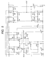
- Fig. 5 is a circuit diagram showing the switches and so forth by using MOS transistors in accordance with the above-mentioned embodiment in more detail, and the basic structure of the circuit is identical with the structure of Fig. 1, in which MOS transistors M15 to M19 correspond to the switches SW5, SW6, SW1, SW2 and SW7 in Fig. 4.
- MOS transistors M20 and M21' are transistors that function as current sources, and a MOS transistor M22' is a voltage source that gives the gate biases of the MOS transistors M11 and M12.
- the switch SW7 of the MOS transistor M19 may be structured as a switch that is not connected in series to the current source M20 but controls the output current per se of the current source M20 as shown in Fig. 5.
- a terminal INN is an inversion input terminal of the amplifier, and INP is a non-inversion input terminal of the amplifier.
- Fig. 6 shows a timing of the circuit shown in Fig. 5.
- the MOS transistor M17 switch SW1
- the MOS transistor M18 is turned on with a delay from the MOS transistor M18 (switch SW2). This is because the MOS transistor M18 is connected to the non-inversion input terminal, there are normally many cases in which the non-inversion input terminal is connected to a certain power source, and therefore a current necessary for raising the source potential of the MOS transistor M18 when the MOS transistor M18 is turned on can be supplied from the current source.
- Fig. 7 shows an output waveform of the circuit shown in Fig. 5 through simulation, in which a top output waveform is a waveform of an output resulting from conducting the above-mentioned switching operation, a middle waveform is a waveform of the top waveform from which a switching noise is removed through a filter, and a bottom waveform is a waveform of a conventional amplifier that is not subjected to switching.
- the respective values may be determined in accordance with the specification required for the amplifier.
- the on/off control of the switches SW is conducted by a drive circuit.
- the differential transistor pair M21 and M22 and the capacitor CL are not electrically connected to each other. Therefore, the influence of the noise, which is generated due to turning on/off of the switches SW1 and SW2, on the signal hold in the capacitor CL is decreased. As a result, it is possible to obtain a signal with high precision.
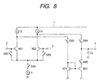
- Fig. 8 is a circuit diagram showing an amplifier in accordance with a second embodiment of the present invention to which the conventional amplifier of the type shown in Fig. 2 is applied.
- Reference symbols I1, I2 and I3 denote constant current source for bias, and the switches SW3 and SW4 function as a common gate stage at the time of L0 and as switch-off at the time of HI by switching by HI/LO (appropriate VREF voltage) the gate potential of the common gate stage in the conventional example shown in Fig. 1.
- the switch SW5 is disposed at the output of the current mirror circuit of the MOS transistors M23 and M24, and functions as a sample/hold circuit in which a load capacitor CL is regarded as a hold capacitor when the switches SW3, SW4 and SW5 are off.
- the switch SW5 may be replaced with control of the gate potentials of the current mirror circuits M23 and M24.
- the cut-off frequency of a low-pass filter connected to the output terminal 4 is set to a value remarkably lower than the band of the amplifier.
- the on/off control of the switch SW is conducted by a drive circuit.
- the differential transistor pair M21 and M22 and the capacitor CL are not electrically connected to each other. Therefore, the influence of the noise, which is generated due to turning on/off of the switches SW1 and SW2, on the signal hold in the capacitor CL is decreased. As a result, it is possible to obtain a signal with high precision.
- Fig. 9 shows a case in which the differential amplifier of the first or second embodiment is applied to a solid state image pickup element in accordance with a third embodiment.
- a noise reducing circuit called "CDS(correlated double sampling)" is used. Therefore, a significance for reducing the 1/f noise by using the differential amplifier for the solid state image pickup element is large.
- Reference numeral 41 denotes sensor cells which are arranged two-dimensionally as one example.
- Reference numerals 42-1, 42-2, ..., 42-m denote select signal lines that select rows of the sensor cells. The select signal lines are driven by a vertical shift register 48.
- Reference numerals 43-1, 43-2, ..., 43-n denote vertical signal lines, and the signals of the respective sensor cells 41 selected by the select signal lines 42-1 to 42-m appear in the vertical signal lines 43-1 to 43-n.
- Reference numerals 44-1, 44-2, ..., 44-n denote horizontal transfer switches which are driven by a horizontal shift register 47, and sequentially read the signal that appear in the vertical signal lines 43-1 to 43-n to a horizontal signal line 45 by sequentially turning on the horizontal transfer switches 44-1 to 44-n.
- the signal read into the horizontal signal line 45 is amplified by a differential amplifier 49 of the present invention, and then outputted from an output terminal 50. Switching operation for reducing the 1/f noise is conducted within the differential amplifier 49 at any time, and a low pass filter may be further connected to the output terminal 10 for the purpose of suppressing the switching noise.
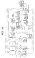
- a fourth embodiment of the present invention in the case where a solid state image pickup element according to the third embodiment is applied to the video camera will be described in detail with reference to Fig. 10.
- Reference numeral 51 denotes a photographing lens that includes a focus lens 51A for adjusting a focal point, a zoom lens 51B that conducts the zoom operation, and an imaging lens 51C.
- Reference numeral 52 denotes an iris
- 53 denotes a solid state image pickup element that photoelectrically converts an image of the object which is imaged on a photographing plane into an electric image pickup signal
- 54 denotes a sample/hold circuit (S/H circuit) that samples and holds the image pickup signal outputted from the solid-state image pickup element 53 and also amplifies the level to output the video signal.
- S/H circuit sample/hold circuit
- Reference numeral 55 denotes a process circuit that subjects the video signal outputted from the sample/hold circuit 54 to given processes such as gamma correction, color separation, and blanking processing, to output a luminance signal Y and a chroma signal C.
- the chroma signal C outputted from the process circuit 55 is subjected to corrections of white balance and color balance by a chrominance signal correction circuit 71 and then outputted to an encoder circuit (ENC circuit) 74 and a gate circuit 75 as color difference signals R-Y and B-Y.
- An output of the gate circuit 75 is inputted to an integral circuit 75, and an output of the integral circuit 75 is inputted to a logical control circuit 67.
- the luminance signal Y outputted from the process circuit 55 and the color difference signals R-Y and B-Y outputted from the chrominance signal correction circuit 71 are modulated by the encoder circuit (ENC circuit) 74 and then outputted as standard television signals. Then, those signals are supplied to a monitor EVF such as a video recorder or an electronic view finder (not shown).
- EVF such as a video recorder or an electronic view finder (not shown).
- reference numeral 56 denotes an iris control circuit that controls the iris drive circuit 57 on the basis of the video signal supplied from the sample/hold circuit 54 and automatically controls an ig meter 58 to control the opening degree of the iris 52 so that a level of the video signal becomes a fixed value of a given level.
- Reference numerals 63 and 64 denote band pass filters (BPFs) having different band limits which extract high frequency components necessary to conduct focus detection from the video signals outputted from the sample/hold circuit 54.
- Signals outputted from the first band pass filter 63 (BPF1) and the second band pass filter 64 (BPF2) are gated by a gate circuit 65 and a focus gate frame signal, respectively, and a peak value is detected and held by a peak detection circuit 66 and also inputted to the logical control circuit 67. This signal is called “focal point voltage", and focusing is made by the focal point voltage.
- the logical control circuit 67 is connected to a gate pulse generation circuit 73, and the gate pulse generation circuit 73 sends pulses to the gate circuits 65 and 72.
- reference numeral 68 denotes a focus encoder that detects the moving position of the focus lens 51A
- 69 denotes a zoom encoder that detects the focal point distance of the zoom lens 51B
- 70 denotes an iris encoder that detects the opening degree of the iris 52.
- the detected value of the encoder 70 is supplied to the logical control circuit 67 that conducts system control.
- the logical control circuit 67 conducts the focus detection with respect to the object on the basis of the video signal corresponding within a set focus detection region to adjust the focal point.
- the logical control circuit 67 takes in the peak value information of the high frequency component supplied from the respective band pass filters 63 and 64, and supplies control signals of the rotating direction, the rotating speed, the rotation/stop and so forth of a focus motor 60 to a focus drive circuit 59 so as to drive the focus lens 51A to a position at which the peak value of the high frequency component becomes maximum, and controls the focus drive circuit 59. Also, the logical control circuit 67 supplies the control signal of a zoom motor 62 to a zoom drive circuit 61 so as to drive the zoom lens 51B and controls the zoom drive circuit.
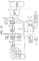
- reference numeral 81 denotes a barrier that serves as the protector of the lens and a main switch
- 82 denotes a lens that forms the optical image of the object onto a solid-state image pickup element 84
- 83 denotes an iris for varying the quantity of light that passes through the lens 82
- 84 denotes a solid-state image pickup element for taking in the object image which is formed by the lens 82 as an image signal
- 85 denotes an image signal processing circuit that processes the image signal outputted from the solid-state image pickup element 84
- 86 denotes an A/D conversion circuit that conducts analog/digital conversion of the image signal outputted from the image signal processing circuit 85
- 87 denotes a signal processing unit that conducts various corrections on the image data outputted from the A/D conversion circuit 86 and compresses the data
- 88 denotes a timing generation unit that outputs various timing signals to the solid-state image pickup element 84, the image signal processing circuit 85, the A/D conversion circuit
- the operation of the thus-structured still video camera thus structured at the time of photographing will be described.
- the main power supply is turned on, and subsequently, a power supply for the control system is turned on, and also a power supply for the image pickup system circuit such as the A/D conversion circuit 86 is turned on.
- the system control and operation unit 89 releases the iris 83, and the signal outputted from the solid-state image pickup element 84 is converted by the A/D conversion circuit 86 through the image signal processing circuit 85 and then inputted to the signal processing unit 87.
- the calculation of the exposure is conducted by the system control and operation unit 89 on the basis of that data.
- the brightness is judged on the basis of the result of photometry, and the system control and operation unit 89 controls the iris 83 in accordance with the result. Then, the system control and operation unit 89 extracts the high frequency component and calculates a distance to the object on the basis of the signal outputted from the solid-state image pickup element 84. Thereafter, the system control and operation unit 89 drives the lens 82 to judge whether focusing is made or not, and when it is judged that focusing is not made, the lens 82 is again driven to conduct the range finding. Then, after the focusing is recognized, actual exposure starts.
- the image signal outputted from the solid-state image pickup element 84 is A/D converted by the A/D conversion circuit 86 through the image signal processing circuit 85, passes through the signal processing unit 87 and is then written in the memory unit 90 by the system control and operation unit 89. Thereafter, the data stored in the memory unit 90 passes through the recording medium control I/F unit 91 and is recorded in the detachably attachable recording medium 92 such as a semiconductor memory under the control by the system control and operation unit 89. Also, the data may be inputted directly to the computer or the like through an external I/F unit 93 to process the image.
- FIG. 12 is a schematic diagram showing an original image reading device that reads an original image.
- Reference numeral 101 denotes a contact type image sensor (hereinafter also called "CIS") which is composed of a solid-state image pickup element 102, a cell fok lens 103, an LED array 104 and a contact glass 105.
- Feed rollers 106 are disposed in front of and at the back of the CIS 101, and used for arranging an original.
- a contact sheet 107 is used to bring the original in contact with the CIS 101.
- Reference numeral 110 denotes a control circuit that processes a signal from the CIS 101.
- An original detection lever 108 is a lever for detecting that the original is inserted thereinto, and when the original detection lever 108 detects that the original is inserted, the original detection lever 108 is inclined to change an output of the original detection sensor 109. Then, this state is transmitted to a CPU 215 within the control circuit 110, and it is judged that the original is inserted, and a drive motor of the original feed rollers 106 (not shown) is driven to start the original feeding to conduct the reading operation.
- Fig. 13 is a block diagram showing an electric structure for explaining the control circuit 110 shown in Fig. 12 in detail. Hereinafter, the circuit operation will be described with reference to Fig. 13.
- reference numeral 201 denotes an image sensor (CIS 101 shown in Fig. 12) which is integrated with LEDs 202 of the respective colors R, G and B which are light sources.
- the image sensor 201 can sequentially read the color images of R, G and B lines by switchingly turning on the LEDs 202 of the respective colors R, G and B for each line by an LED control (drive) circuit 203 while the original is fed on the contact glass 105 of the CIS 101.
- Reference symbol AMP204 denotes an amplifier that amplifies a signal outputted from the CIS 201
- 205 denotes an A/D conversion circuit that A/D converts the amplified output to obtain a digital output of, for example, 8 bits.
- a shading RAM 206 stores therein shading correction data by reading a calibration sheet in advance, and a shading correction circuit 207 conducts the shading correction of the read image signal read on the basis of the data of the shading RAM 206.
- a peak detection circuit 208 is a circuit that detects a peak value of the read image data for each line and is used for detecting a leading edge of the original.
- a gamma conversion circuit 209 conducts the gamma conversion of the read image data in accordance with a gamma curve predetermined by a host computer.
- a buffer RAM 210 is a RAM for temporarily storing the image data in order to synchronize timings of the actual reading operation and the host computer in communication with each other, and a packing/buffer RAM control circuit 211, after conducting a packing process in accordance with image output modes (binary value, 4-bit multi-value, 8-bit multi-value, 24-bit multi-value) predetermined by the host computer, writes the data in the buffer RAM 210 and reads the image data in an interface circuit 212 from the buffer RAM 210 to output the data.
- the interface circuit 212 receives a control signal and also outputs the image signal with respect to an external apparatus 213 which is the host device of the image reading device of this embodiment, for example, the personal computer.
- Reference numeral 215 denotes, for example, a CPU in the form of a microcomputer, which includes a ROM 215A that stores a processing procedure therein and a RAM 215B for operation, and controls the respective units in accordance with the procedure stored in the ROM 215A.
- Reference numeral 216 denotes, for example, a crystal oscillator
- 214 denotes a timing signal generation circuit that divides the output of the oscillator 216 in accordance with the setting of the CPU 215 and generates various timing signals which are used as references of the operation.
- Reference numeral 213 denotes an external apparatus connected with the control circuit through the interface circuit 212, and a personal computer may be cited as an example of the external device.
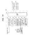
- a seventh embodiment in the case where the solid-state image pickup element of the third embodiment is applied to an original image reading device having a communication function or the like will be described in detail with reference to Figs. 14 and 15.
- Fig. 14 is a block diagram showing the structure of an image processing unit of the image reading device.
- a reader unit 301 reads an original image (not shown), and outputs the image data corresponding to the original image to a printer unit 302 and an image input/output control unit 303.
- the printer unit 302 records the image corresponding to the image data from the reader unit 301 and the image input/output control unit 303 on a recording sheet.
- the image input/output control unit 303 is connected to the reader unit 301 and is composed of a facsimile unit 304, a file unit 305, a computer interface unit 307, a formatter unit 308, an image memory unit 309, a core unit 310 and so forth.
- the facsimile unit 304 transfers the image data resulting from extending the compressed image data received through a telephone line 313 to the core unit 310, and also transmits a compressed image data resulting from compressing the image data transferred from the core unit 310 through the telephone line 313.
- the facsimile unit 304 is connected with a hard disk 312 so as to temporarily save the received compressed image data.
- the file unit 305 is connected with a magneto-optical disk drive unit 306, and the file unit 305 compresses the image data transferred from the core unit 310 and stores the image data together with a keyword for retrieving the image data in the magneto-optical disk arranged in the magneto-optical disk drive unit 306. Also, the file unit 305 retrieves the compressed image data stored in the magneto-optical disk on the basis of the keyword transferred through the core unit 310. Then, the file unit 305 reads and extends the retrieved compressed image data and transfers the extended image data to the core unit 310.
- the computer interface unit 307 is an interface between a personal computer or a workstation (PC/WS) 311 and the core unit 310.
- the formatter unit 308 develops code data that represents the image transferred from the PC/WS 311 to the image data that can be recorded in the printer unit 302, and the image memory unit 309 temporarily stores the data transferred from the PW/WS 311.
- the core unit 310 controls the flow of data between the reader unit 301, the facsimile unit 304, the file unit 305, the computer interface unit 307, the formatter unit 308 and the image memory unit 309.
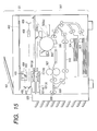
- Fig. 15 is a diagram showing the sectional structures of the reader unit 301 and the printer unit 302 shown in Fig. 14.
- an original supply device 401 of the reader unit 301 feeds an original (not shown) onto a platen glass 402 from a last page one by one in order, and discharges the original on the platen glass 402 after the original reading operation is completed.
- the reader unit 301 turns on a lamp 403, starts the movement of a scanner unit 404 to scan the original with exposure.
- a reflected light from the original due to the exposure scanning is guided to a solid-state image pickup element 409 by mirrors 405, 406, 407 and a lens 408.
- the scanned original image is read by the solid-state image pickup element 409.
- the image data outputted from the solid-state image pickup element 409 is transferred to the printer unit 302 or the core unit 310 after being subjected to a process such as A/D conversion or shading correction.
- Laser drivers 521(a) and 521(b) of the printer unit 302 drive laser emitting units 501(a) and 501(b), and cause the laser emitting units 501(a) and 501(b) to emit laser beams corresponding to the image data outputted from the reader unit 301.
- the laser beams are irradiated onto different positions of a photosensitive drum 502, and latent images corresponding to those laser beams are formed on the photosensitive drum 502.
- a developer is adhered to the portions of the latent images on the photosensitive drum 502 by developing machine 503(a) and 503(b).
- the recording sheet is fed from any one of a cassette 504 and a cassette 505 at a timing which is in synchronism with the start of the laser beam irradiation, and is transferred to a transfer unit 506 and the developer adhered to the photosensitive drum 502 is transferred onto the recording sheet.
- the recording sheet on which the developer is deposited is fed onto a fixing unit 507, and the developer is fixed onto the recording sheet due to a heat and a pressure in the fixing unit 507.
- the recording sheet that has passed through the fixing unit 507 is discharged by a discharge roller 508, and a sorter 520 receives the discharged recording sheets into the respective pins and sorts the recording sheets.
- the sorter 520 In the case where sorting is not set, after the sorter 520 feeds the recording sheet to the discharge roller 508, the sorter 520 reverses the rotating direction of the discharge roller 508 and then guides the recording sheet to a sheet re-feed path 510 by a flapper 509. Also, in the case where the multiple recording is not set, the recording sheet is guided to the sheet re-feed path 510 by the flapper 509 in such a manner that the recording sheet is not fed to the discharge roller 508. The recording sheet guided to the re-feed path 510 is supplied to the transfer unit 506 at the same timing as the above-mentioned timing.
- a camera control system having a video camera of the fourth embodiment using the solid-state image pickup element of the third embodiment will be described in detail with reference to Fig. 16 in accordance with an eighth embodiment of the present invention.
- This embodiment is not limited to the video camera of the fourth embodiment but may be directed to the still camera of the fifth embodiment using the solid-state image pickup element of the third embodiment.
- Fig. 16 is a block diagram showing the rough structure of a camera control system.
- Reference numeral 710 denotes a network that transmits video data and camera control information (including status information) in a digital format and is connected with n image transmitting terminals 712 (712-1 to 712-n).
- the respective image transmitting terminals 712 (712-1 to 712-n) are connected with video cameras 716 (716-1 to 716-n) through camera control devices 714 (714-1 to 714-n).
- the camera control devices 714 (714-1 to 714-n) control the pan, tilt, zoom, focus, iris and the like of the connected video cameras 716 (716-1 to 716-n) in accordance with the control signals from the image transmitting terminals 712 and the video cameras 716 (716-1 to 716-n). Also, the video cameras 716 (716-1 to 716-n) are applied with power supply from the camera control devices 714 (714-1 to 714-n), and the camera control devices 714 (714-1 to 714-n) control the on/off operation of the power supply of the video cameras 716 (716-1 to 716-n) in accordance with a control signal from the external.
- the network 710 is connected with image reception terminals 718 (718-1 to 718-m) that receive the image information sent from the image transmitting terminals 712 (712-1 to 712-n) to the network 710 and display the image information.
- the respective image reception terminals 718 (718-1 to 718-m) are connected with monitors 720 (720-1 to 720-m) each composed of a bit map display, a CRT or the like.
- the network 710 does not need to be wired, but may be a wireless network using a wireless LAN device.
- the image reception terminal 718 may be a portable image reception terminal device integrated with the monitor 720.
- the image transmitting terminals 712 compress the output video signals of the connected video cameras 716 (716-1 to 716-n) by given compression systems such as H.261 or the like and transmit the compressed video signals to an image requesting image reception terminal 718 or all of the image reception terminals 718.
- the image reception terminals 718 can control the on/off operation of the power supply together with various parameters (photograph orientation, photograph magnification, focus, iris, etc.) of an arbitrary camera 716 through the network 710, the image transmitting terminals 712 and the camera control device 714.
- the image transmitting terminal 712 may be connected with a monitor and provided with an image extension device that extends the compression image so as to also serve as the image reception terminal.
- the image reception terminals 718 may be connected with the camera control devices 714 and the video cameras 716 and provided with the image compression devices so as to also function as the image transmitting terminals.
- Those terminals are provided with ROMs that store software necessary to transmit or receive the image.
- the image transmitting terminals 712 transmit the video signals to the image reception terminals 718 that is at a remote location through the network 710, and receive the camera control signals transmitted from the image reception terminals 718 to execute the control of the pan, tilt and so forth of the video cameras 716. Also, the image reception terminals 718 send the camera control signals to the image transmitting terminals 712, and the image transmitting terminals 712 that receive the camera control signals control the video cameras 716 in accordance with the contents of the camera control signal and return the present status of the video cameras 716. The image reception terminals 718 receive the video data transmitted from the image transmitting terminals 712 and perform a predetermined processing on the video data to display the picked-up image on the display screens of the monitor 720 in real time.
- connection of the control electrode and the main electrode of the input transistor which is a main 1/f noise source in the amplifier is turned on/off by the switch, and the switching noise that appears in the output of the differential amplifier due to the above switching is more reduced while the 1/f noise per se of the input transistor is reduced with the advantages in that a change in the electric characteristic of the differential amplifier, the power consumption, an increase in the size of the input transistor, and so on are eliminated.
Landscapes
- Engineering & Computer Science (AREA)
- Multimedia (AREA)
- Signal Processing (AREA)
- Physics & Mathematics (AREA)
- Nonlinear Science (AREA)
- Transforming Light Signals Into Electric Signals (AREA)
- Amplifiers (AREA)
- Studio Devices (AREA)
Applications Claiming Priority (2)
| Application Number | Priority Date | Filing Date | Title |
|---|---|---|---|
| JP2000385508A JP2002185260A (ja) | 2000-12-19 | 2000-12-19 | 増幅器及び撮像装置 |
| JP2000385508 | 2000-12-19 |
Publications (2)
| Publication Number | Publication Date |
|---|---|
| EP1220449A2 true EP1220449A2 (de) | 2002-07-03 |
| EP1220449A3 EP1220449A3 (de) | 2005-04-13 |
Family
ID=18852761
Family Applications (1)
| Application Number | Title | Priority Date | Filing Date |
|---|---|---|---|
| EP01310458A Withdrawn EP1220449A3 (de) | 2000-12-19 | 2001-12-14 | Verstärker |
Country Status (3)
| Country | Link |
|---|---|
| US (1) | US6559719B2 (de) |
| EP (1) | EP1220449A3 (de) |
| JP (1) | JP2002185260A (de) |
Cited By (1)
| Publication number | Priority date | Publication date | Assignee | Title |
|---|---|---|---|---|
| GB2414132A (en) * | 2004-05-10 | 2005-11-16 | Agilent Technologies Inc | CMOS image sensor |
Families Citing this family (13)
| Publication number | Priority date | Publication date | Assignee | Title |
|---|---|---|---|---|
| JP4681767B2 (ja) * | 2001-07-17 | 2011-05-11 | キヤノン株式会社 | 撮像装置およびカメラ |
| US6768348B2 (en) | 2001-11-30 | 2004-07-27 | Semiconductor Energy Laboratory Co., Ltd. | Sense amplifier and electronic apparatus using the same |
| US6867652B1 (en) * | 2003-09-09 | 2005-03-15 | Texas Instruments Incorporated | Fast-response current limiting |
| US7088146B1 (en) * | 2004-11-03 | 2006-08-08 | National Semiconductor Corporation | Apparatus and method for high-speed half-latch with low overdrive voltage |
| US20060268140A1 (en) * | 2005-05-24 | 2006-11-30 | Micron Technology, Inc. | Method and apparatus for reducing noise in analog amplifier circuits and solid state imagers employing such circuits |
| KR101109188B1 (ko) | 2005-12-27 | 2012-01-30 | 삼성전자주식회사 | Cmos 증폭기의 플릭커 노이즈를 줄이는 장치 및 방법 |
| US7336129B2 (en) * | 2006-01-24 | 2008-02-26 | Broadcom Corporation | Analog amplitude detector |
| KR100833186B1 (ko) | 2006-10-18 | 2008-05-28 | 삼성전자주식회사 | 증폭 회로, 및 증폭 회로의 바이어스 전압 발생 방법 |
| JP4854626B2 (ja) * | 2007-08-27 | 2012-01-18 | オンセミコンダクター・トレーディング・リミテッド | 低コンダクタアンプ |
| US7532037B1 (en) * | 2008-05-05 | 2009-05-12 | International Business Machines Corporation | Enhanced CML driver circuit for “quiet-driver” measurement enablement |
| IT1403945B1 (it) * | 2011-02-17 | 2013-11-08 | St Microelectronics Srl | Comparatore di una differenza di tensioni di ingresso con almeno una soglia |
| US8829996B1 (en) * | 2013-04-03 | 2014-09-09 | Silicon Laboratories Inc. | High voltage MOS input stage |
| KR102547878B1 (ko) * | 2018-05-11 | 2023-06-27 | 엘지이노텍 주식회사 | 카메라 모듈 및 이의 동작 방법 |
Family Cites Families (7)
| Publication number | Priority date | Publication date | Assignee | Title |
|---|---|---|---|---|
| JP3061923B2 (ja) | 1992-02-28 | 2000-07-10 | キヤノン株式会社 | 半導体発光素子の駆動回路 |
| US5621339A (en) * | 1993-09-14 | 1997-04-15 | Crystal Semiconductor | Method and apparatus for removing trapped oxide charge from a differential input stage |
| US6008670A (en) * | 1997-08-19 | 1999-12-28 | Hewlett-Packard | Differential CMOS logic family |
| US5942922A (en) * | 1998-04-07 | 1999-08-24 | Credence Systems Corporation | Inhibitable, continuously-terminated differential drive circuit for an integrated circuit tester |
| US6087873A (en) * | 1998-07-21 | 2000-07-11 | Motorola, Inc. | Precision hysteresis circuit |
| US6275107B1 (en) * | 1998-10-29 | 2001-08-14 | Fujitisu Limited | Differential amplifier circuit and pull up-type differential driver |
| US6157257A (en) * | 1999-06-30 | 2000-12-05 | Conexant Systems, Inc. | Low power folding amplifier |
-
2000
- 2000-12-19 JP JP2000385508A patent/JP2002185260A/ja active Pending
-
2001
- 2001-12-12 US US10/012,389 patent/US6559719B2/en not_active Expired - Fee Related
- 2001-12-14 EP EP01310458A patent/EP1220449A3/de not_active Withdrawn
Cited By (2)
| Publication number | Priority date | Publication date | Assignee | Title |
|---|---|---|---|---|
| GB2414132A (en) * | 2004-05-10 | 2005-11-16 | Agilent Technologies Inc | CMOS image sensor |
| GB2414132B (en) * | 2004-05-10 | 2009-10-14 | Agilent Technologies Inc | CMOS image sensor |
Also Published As
| Publication number | Publication date |
|---|---|
| EP1220449A3 (de) | 2005-04-13 |
| US6559719B2 (en) | 2003-05-06 |
| JP2002185260A (ja) | 2002-06-28 |
| US20020075070A1 (en) | 2002-06-20 |
Similar Documents
| Publication | Publication Date | Title |
|---|---|---|
| JP4681767B2 (ja) | 撮像装置およびカメラ | |
| JP3962561B2 (ja) | 固体撮像装置及びそれを用いた撮像システム | |
| JP3870088B2 (ja) | 固体撮像装置及びシステム | |
| US7394492B2 (en) | Solid state image pickup device, method of driving solid state image pickup device, and camera using the solid state image pickup device | |
| JP3880345B2 (ja) | 差動増幅回路及びそれを用いた固体撮像装置並びに撮像システム | |
| CN100409448C (zh) | 摄像设备和包括摄像设备的摄像机系统 | |
| US7671907B2 (en) | Image-capturing apparatus | |
| US6559719B2 (en) | Amplifier | |
| JP4013700B2 (ja) | 撮像装置 | |
| US6963368B1 (en) | Digital camera and image capturing control apparatus including a delay device | |
| EP1067766B1 (de) | Bildaufnahmegerät | |
| US5563658A (en) | Electronic camera with rapid automatic focus of an image upon an image sensor | |
| JPH09238286A (ja) | デジタル光学センサ | |
| JPH10190988A (ja) | 画像読み取り装置 | |
| JP2002530942A (ja) | 複数のイメージキャプチャモードを有する画像処理システム | |
| JP3948433B2 (ja) | 固体撮像装置 | |
| US6867409B2 (en) | Solid-state image sensing device | |
| JP4154068B2 (ja) | 固体撮像装置及びそれを用いた撮像システム及び画像読取システム | |
| US20060072025A1 (en) | Solid-state image sensing device and image sensing device including the solid-state image sensing device | |
| JP4735051B2 (ja) | 撮像装置 | |
| JP2004289821A (ja) | 画像入力装置 | |
| JP2001218113A (ja) | 固体撮像装置 | |
| US20060268154A1 (en) | Image pickup apparatus | |
| JPH05207306A (ja) | 画像読取装置 | |
| US20030035152A1 (en) | Scanning method with two exposure steps |
Legal Events
| Date | Code | Title | Description |
|---|---|---|---|
| PUAI | Public reference made under article 153(3) epc to a published international application that has entered the european phase |
Free format text: ORIGINAL CODE: 0009012 |
|
| AK | Designated contracting states |
Kind code of ref document: A2 Designated state(s): AT BE CH CY DE DK ES FI FR GB GR IE IT LI LU MC NL PT SE TR |
|
| AX | Request for extension of the european patent |
Free format text: AL;LT;LV;MK;RO;SI |
|
| PUAL | Search report despatched |
Free format text: ORIGINAL CODE: 0009013 |
|
| AK | Designated contracting states |
Kind code of ref document: A3 Designated state(s): AT BE CH CY DE DK ES FI FR GB GR IE IT LI LU MC NL PT SE TR |
|
| AX | Request for extension of the european patent |
Extension state: AL LT LV MK RO SI |
|
| RIC1 | Information provided on ipc code assigned before grant |
Ipc: 7H 03K 19/003 B Ipc: 7H 04N 5/217 B Ipc: 7H 03K 5/02 B Ipc: 7H 03K 5/24 A |
|
| 17P | Request for examination filed |
Effective date: 20050826 |
|
| AKX | Designation fees paid |
Designated state(s): DE FR GB IT NL |
|
| 17Q | First examination report despatched |
Effective date: 20100316 |
|
| STAA | Information on the status of an ep patent application or granted ep patent |
Free format text: STATUS: THE APPLICATION HAS BEEN WITHDRAWN |
|
| 18W | Application withdrawn |
Effective date: 20100707 |