EP1220450A2 - Integrierte Halbleiterschaltung - Google Patents
Integrierte Halbleiterschaltung Download PDFInfo
- Publication number
- EP1220450A2 EP1220450A2 EP01310696A EP01310696A EP1220450A2 EP 1220450 A2 EP1220450 A2 EP 1220450A2 EP 01310696 A EP01310696 A EP 01310696A EP 01310696 A EP01310696 A EP 01310696A EP 1220450 A2 EP1220450 A2 EP 1220450A2
- Authority
- EP
- European Patent Office
- Prior art keywords
- circuit
- logic
- output
- semiconductor integrated
- nmisfet
- Prior art date
- Legal status (The legal status is an assumption and is not a legal conclusion. Google has not performed a legal analysis and makes no representation as to the accuracy of the status listed.)
- Granted
Links
Images


Classifications
-
- H—ELECTRICITY
- H03—ELECTRONIC CIRCUITRY
- H03K—PULSE TECHNIQUE
- H03K19/00—Logic circuits, i.e. having at least two inputs acting on one output; Inverting circuits
- H03K19/0008—Arrangements for reducing power consumption
- H03K19/0016—Arrangements for reducing power consumption by using a control or a clock signal, e.g. in order to apply power supply
Definitions
- This invention relates to a semiconductor integrated circuit which has a plurality of power supply levels and causes logic circuits to operate on a very low power supply voltage, and more particularly to a semiconductor integrated circuit provided with an operating circuit and a standby circuit.
- the characteristics of the transistors deteriorate due to the generation of hot carriers, or the breakdown of the insulating films occurs due to TDDB (Time-Dependent Dielectric Breakdown).
- TDDB Time-Dependent Dielectric Breakdown
- the generation of hot carriers is prevented by weakening the horizontal electric field between the source and drain, and TDDB is prevented by weakening the vertical electric field between the gate and bulk.
- dropping the power supply voltage decreases the reverse bias applied to the junction between the source and bulk and to the junction between the drain and bulk, thereby coping with a drop in the breakdown voltage.
- a lightweight power supply with a high energy density such as a lithium ion battery
- a lithium ion battery Since the voltage of the lithium ion battery is about 3 V, it is higher than the breakdown voltage of the very small MOS transistor. Therefore, when the lithium ion battery is applied to a circuit using very small transistors, it is necessary to drop its voltage using a DC-DC voltage converter. Since the power consumption of the CMOS circuit used in a logic circuit is proportional to the operating frequency and further proportional to the square of the power supply voltage, lowering the power supply voltage has a significant effect on the decrease of the chip power consumption.
- Using mobile information apparatus for a longer time requires a battery with high energy density, a DC-DC converter with high efficiency, and an integrated circuit operating on a low voltage. From the viewpoint of reducing the power consumption of an LSI, it is desirable to use a stepped-down power supply voltage particularly in a microprocessor or baseband LSI which consumes a lot of power.
- the mobile information apparatus requires memory elements, such as DRAMs or SRAMs (static random access memories) as well as the logic circuits.
- DRAMs the first subject is to secure a sufficient amount of charge in the cells to increase resistance to errors due to software.
- SRAMs the first subject is to avoid the deterioration of speed when they are operating on low power supply voltages. Therefore, in DRAMs and SRAMs, the power consumption has not been reduced remarkably as found in logic circuits. Presently, elements operating on a power supply voltage of about 1.5 V have been put to practical use.
- the power supply voltage of about 1.5 V is much higher than the lowest voltage on which the logic circuits can operate. For this reason, it is conceivable that an LSI including both memory circuits and logic circuits takes and will take a multi-power-supply configuration that supplies various power supply voltages according to each circuit section.
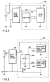
- FIG. 1 shows a semiconductor integrated circuit for mobile information apparatus obtained by integrating a memory circuit and a logic circuit into a single chip and the configuration of its power supply.
- the power supply system is composed of a lithium ion battery 1700 and a DC-DC voltage converter 1701.
- the semiconductor integrated circuit 1704 is composed of a logic circuit 1702 and an on-chip memory circuit 1703.
- 3 V from the lithium ion battery 1700 is converted by the DC-DC voltage converter 1700 into a voltage of 0.5 V.
- the 0.5-V power supply is supplied to the logic circuit 1702.
- the on-chip memory circuit 1703 generally needs a power supply voltage of 1.5 to 2.0 V or higher for high speed operation, the 3-V power supply of the lithium ion battery 1700 is supplied to the memory circuit 1703.
- dropping the power supply voltage of the logic circuit from 3V to about 0.5 V enables the power consumption in operation to be decreased theoretically by about 95%, which reduces the power consumption dramatically.
- the threshold voltage of the MOS transistors is dropped as the power supply voltage drops.
- a MOSFET whose threshold voltage is about 0.1 to 0.15 V in absolute value, about one-third of the threshold voltage of a conventional MOSFET.
- the S factor that determines the sub-threshold characteristic of, for example, a MOSFET is 100 mV/decade, the leakage current when the MOSFET is off increases significantly by about three orders of magnitude.
- the semiconductor integrated circuit is unsuitable for mobile information apparatus as it is.
- FIG. 2 shows a known semiconductor integrated circuit configured to overcome the above problem.
- a power supply voltage converter 1801 converts 3 V from a lithium ion battery 1800 into a voltage of 0.5 V to supply the voltage as low as 0.5 V to a semiconductor integrated circuit 1805 including a logic circuit 1802, thereby reducing the power consumption in operation.
- the semiconductor integrated circuit 1805 further comprises a positive power supply voltage generator 1803 and a negative power supply voltage generator 1804 and generates a potential higher than the power supply voltage at the positive power supply voltage generator 1803 and a potential lower than the ground potential at the negative power supply voltage generator 1804.
- the semiconductor integrated circuit is configured to supply the potentials generated at the voltage generators to the n-well and p-well (now shown) in the logic circuit 1802, thereby making somewhat lower the absolute value of the threshold voltage of the MOSFET in the logic circuit in normal operation to give priority to the operating speed.
- the power consumption can be reduced by making larger the absolute value of the threshold voltage of the MOSFET in the logic circuit in the standby state to decrease the leakage current when the MOSFET is off.
- a charge pump method is generally used in the positive power supply voltage generator 1803 and negative power supply voltage generator 1804.
- an ordinary charge pump method cannot provide a sufficient driving capability to control the well potential.
- An attempt to increase the driving capability makes the size of the driving MOSFET very large, with the result that the layout area of the voltage generators is larger than that of conventional equivalents.
- FIG. 3 is a diagram to help explain a leakage current problem occurring in the off state.
- three kinds of power supply are supplied to a semiconductor integrated circuit 1905.
- a 3-V power supply (VDD) supplied from a nickel-hydrogen battery 1900 and the ground potential (VSS) are connected to a logic circuit 1902 integrated in an on-chip manner in the semiconductor integrated circuit.
- a logic circuit power supply VD1 (0.5 V) supplied from a power supply voltage converter 1901 is connected via a pMOSFET 1093 with a high threshold value to a logical circuit power supply line VDDV.
- the gate voltage (/STB) of the pMOSFET 1903 is made VDD and the MOSFET 1903 is brought into the off state.
- the leakage current is determined at a very small value by the off characteristic of the pMOSFET 1903 with a high threshold value.
- Methods of making lower the power consumption in the standby state include a well potential control method of generating a voltage higher than the power supply voltage of the logic circuit in the semiconductor integrated circuit and a potential lower than the ground potential on the chip and thereby controlling the well potential and a power supply switching method of constructing a power supply switch using FETs with good off characteristics.
- such a semiconductor integrated circuit has been desired as is capable of realizing a lower power consumption in both the operating and standby states in a logic circuit operating on a very low power supply voltage of about 0.5 V without using a complex control circuit.
- a semiconductor integrated circuit comprising: a first logic circuit which has a first input terminal and comprises a logic block that essentially connects a first pMIS logic block made up of a pMISFET with a threshold voltage of Vtp1 and a first nMIS inverted-logic block made up of an nMISFET with a threshold voltage of Vtn1 in series between a first power supply with a potential of V1 and a reference potential; a second logic circuit which has a second input terminal connected to the first input terminal and which has the same logic function as that of the first logic circuit and comprises a logic block that essentially connects a second pMIS logic block made up of a pMISFET with a threshold voltage of Vtp2 (Vtp2 ⁇ Vtp1) and a second nMIS inverted-logic block made up of an nMISFET with a threshold voltage of Vtn2 (Vtn2 ⁇ Vtn1) in series between a second
- a semiconductor integrated circuit comprising: a first logic circuit which has a first input terminal and comprises a logic block that essentially connects a first pMIS logic block made up of a pMISFET with a threshold voltage of Vtp1 and a first nMIS inverted-logic block made up of an nMISFET with a threshold voltage of Vtn1 in series between a first power supply with a potential of V1 and a reference potential; a second logic circuit with a second input terminal which has a different logic function from that of the first logic circuit and which comprises a logic block that essentially connects a second pMIS logic block made up of a pMISFET with a threshold voltage of Vtp2 (Vtp2 ⁇ Vtp1) and a second nMIS inverted-logic block made up of an nMISFET with a threshold voltage of Vtn2 (Vtn2 ⁇ Vtn1) in series between a second power supply with a potential
- FIG. 4 is a block diagram showing the basic configuration of a semiconductor integrated circuit 100 according to a first embodiment of the present invention.
- Two power supplies 102 and 103 which fulfill the expression V1 > V2, supply voltages not only to the semiconductor integrated circuit 100 but also to an internal logic circuit 101.
- the internal logic circuit 101 is composed of a first and a second logic circuit 104 and 105, which have the same logic function.
- the first logic circuit 104 includes a pMOS circuit block 106 and an nMOS circuit block 108 having a complementary logic to the pMOS circuit block 106.
- the second logic circuit 105 includes a pMOS circuit block 107 and an nMOS circuit block 109 having a complementary logic characteristic to the pMOS circuit block 107.
- the output terminals O1 to O4 of the respective blocks are connected to an output terminal Dout via an output switch circuit 110 which effects switching according to a control signal Cont applied to the control terminal of the switch circuit 110.
- the control signal Cont connects the output terminals O2 and O4 of the pMOS circuit block 107 and nMOS circuit block 109 to the output terminal Dout, thereby achieving a low power consumption operation at a low voltage.
- an output switching signal connects the output terminals O1 and O3 of the pMOS circuit block 106 and nMOS circuit block 108 in the first logic circuit 104 to the output terminal Dout. Since both of the pMOS circuit block 106 and nMOS circuit block 108 are composed of transistors whose threshold voltages have relatively large absolute values, the first logic circuit 104 has a low leakage current characteristic.
- the semiconductor integrated circuit presents a low power consumption characteristic at the low power supply voltage when it is in operation, whereas it presents a low leakage current characteristic when it is in the standby state.
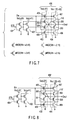
- FIG. 5 shows a concrete example of the output switch circuit 110 used in the first embodiment.
- the drains of pMOSFETs 200 and 202 and nMOSFETs 201 and 203 are connected to the output terminal Dout.
- the sources of the pMOSFETs 200 and 202 and nMOSFETs 201 and 203 are connected to the output terminals O1 to O4 of the pMOS circuit blocks 106 and 107 and nMOS block circuits 108 and 109 in FIG. 4, respectively.
- control signal Cont is supplied to the gates of the pMOSFET 200 and nMOSFET 203 and the complementary signal /Cont of the control signal Cont is supplied to the gates of the pMOSFET 202 and nMOSFET 201.
- FIG. 6 shows another concrete example of the output switch circuit 110 used in the first embodiment.
- the drains of pMOSFET 300 and nMOSFETs 301, 303 and the source of the nMOSFET 302 are connected to the output terminal Dout.
- the sources of the MOSFTTs 300, 301 and 303 are connected to the output terminals O1, O3 and O4 of the pMOS circuit block 106 and nMOS circuit blocks 108 and 109, respectively.
- the drain of the nMOSFET 302 is connected to the output terminal O2 of the pMOS circuit block 107 in FIG. 4.
- control signal Cont is supplied to the gates of the pMOSFET 300 and nMOSFETs 302, 303.
- the complementary signal /Cont of the control signal Cont is supplied to the gate of the nMOSFET 301.
- a first switch circuit composed of the pMOSFET 300 and nMOSFET 301 is inserted between the MOS circuit blocks 106 and 108 constituting the first logic circuit 104.
- a second switch circuit composed of the nMOSFETs 302 and 303 is inserted between the MOS circuit blocks 107 and 109 constituting the second logic circuit 105. Then, the first and second switch circuits operate complementarily under the control of the control signals Cont and /Cont.
- this circuit configuration is such that the second switch circuit connected to the blocks 107 and 109 in the second logic circuit 105 is composed of only nMOSFETs, enabling the driving power to be increased.
- FIG. 7 shows a concrete example of a semiconductor integrated circuit according to the first embodiment.
- Inverters 401 and 402 to which a power supply V1 is supplied are inserted to logically produce an output switching control signal and its complementary signal.
- the inverters 401 and 402 output a high level voltage V1 and a low level ground potential.
- the inverters 401 and 402 are composed of FETs whose threshold voltages have high absolute values (or FETs with high threshold values).
- the logic circuit is composed of a first logic circuit 403 connected to the power supply voltage V1 and a second logic circuit 404 connected to a power supply V2 (V1 > V2).
- the output switch circuit 110 of FIG. 5 is connected to an output terminal Dout. Any of the transistors 200 to 203 constituting the output switch circuit 110 is composed of a FET with a high threshold value. In this circuit, since each of the pMOS circuit block and nMOS circuit block is composed of a single transistor, they perform logical inversion (or function as inverters).
- the output of the first logic circuit 403 is disconnected from the output terminal Dout by the nMOSFET 201 and pMOSFET 200 and the output of the second logic circuit 404 is connected to the output terminal Dout.
- the power consumption becomes very low.
- FIG. 8 show another example of the semiconductor integrated circuit according to the first embodiment.
- Inverters 401 and 402 to which a power supply V1 is supplied are inserted to logically produce an output switching control signal and its complementary signal.
- the inverters 401 and 402 output a high level voltage V1 and a low level ground potential.
- the inverters 401 and 402 are composed of FETs whose threshold voltages have high absolute values (or FETs with high threshold values).
- the logic circuit is composed of a first logic circuit 403 connected to the power supply voltage V1 and a second logic circuit 404 connected to a power supply V2 (V1 > V2).
- the output switch circuit 110' of FIG. 6 is connected to the output terminal.
- any of the transistors 300 to 303 constituting the output switch circuit 110' is composed of a FET with a high threshold value.
- each of the pMOS circuit block and nMOS circuit block is composed of a single transistor, they perform logical inversion (or function as inverters).
- the output of the first logic circuit 403 is connected to the output terminal Dout and the output of the second logic circuit 404 is disconnected from the output terminal Dout by the pMOSFETs 302 and 303 which are fully off. Since the amount of leakage current is determined by the leakage characteristics of the FETs 300 and 301 with high threshold values, the amount of leakage current is much smaller than when FETs whose threshold voltages had low absolute values (or FETs with low threshold values) were used in a conventional equivalent.
- the output of the first logic circuit 403 is disconnected from the output terminal by the nMOSFET 301 and pMOSFET 300 and the output of the second logic circuit 404 is connected to the output terminal Dout.
- the power consumption becomes very low.
- FIG. 9 shows an embodiment of the present invention which uses the inverter 400 of FIG. 7 in flip-flops.
- the inverter 400' of FIG. 8 may be used instead.
- Vcc and Vcc-05 are supplied as power supply.
- Vcc and Vcc-05 are supplied to the internal circuit.
- Vcc is supplied to the internal circuit.
- the semiconductor integrated circuit 600 comprises master-slave flip-flops 602 and 603 and an ordinary logic circuit 604.
- Each of the mater-slave flip-flops 602 and 603 is composed of the inverters 400 (or 400') of FIG. 7 (or FIG. 8) and a transfer gate 605 made up of pMOSFET and nMOSFET connected in parallel.
- Vcc-05 can be connected to or disconnected from an internal power supply line Vcc-05-in by an nMOSFET 601 to whose gate a standby signal /STB is inputted.
- the high potential power supply Vcc is supplied to the master-slave flip-flop 602 and 603.
- the internal power supply line Vcc-05-in is supplied to internal logic circuits 602 to 604 each including flip-flops.
- a clock is inputted to the inputs of the transfer gates in the master-slave flip-flops 602 and 603.
- the clock signal is inputted via an AND gate 606 so that the integrated circuit may be off.
- Vcc-05 and Vcc-05-in become equal to each other. Then, since the inverters in the master-slave flop-flops 602 and 603 operate with a logical amplitude of Vcc-05 and the logic circuits in the semiconductor integrated circuit 600 including the logic circuit 604 operate with an amplitude of Vcc-05, enabling a low power consumption operation.
- Vcc-05 is disconnected from Vcc-05-in, with the result that Vcc-05-in approaches the ground potential gradually (see Vcc-05-in of FIG. 10).
- the high level of the logic circuits, such as the logic circuit 604, in the semiconductor integrated circuit 600 approaches the ground potential gradually (see Out in FIG. 10).
- the transfer gate 605 is gated with a clock signal so as to be off in the standby state, putting the high level at Vcc and the low level at the ground potential, which causes the contents of the flip-flop to be held (see Q of FIG. 10).
- the semiconductor integrated circuit changes from the standby state to the operating state, the high level becomes Vcc-05 and the low level becomes the ground potential in the flip-flop, taking a recovering time of several nanoseconds into account, which enables the integrated circuit to operate again (see Q in FIG. 10).
- FIG. 10 shows the potential at each node in the above explanation.
- FIG. 10 particularly shows how the internal power supply Vcc-05-in, the outputs of the master-slave flip-flops 602 and 603, and the output of the logic circuit change in the operating state and in the standby state.
- the FET 601 is assumed to be an nMOS. The same effect can be produced even if the FET 601 is a pMOS controlled by the standby signal STB.
- FIG. 11 shows an example of using 2-input NAND gates.
- Vcc the power supply voltage
- Vcc-05 be 0.5 V on the assumption that it is produced from the DC-DC conversion of Vcc.
- FETs whose conducting paths are represented by thick lines have high threshold values.
- the threshold voltage of an nMOSFET is 0.4 V and that of a pMOSFET is - 0.4 V.
- the other FETs in FIG. 11 have low threshold values.
- the threshold voltage of an nMOSFET is 0.1 V and that of a pMOSFET is - 0.1 V.
- Inverters 401 and 402 are composed of FETs with high threshold values, to which Vcc is supplied.
- the gate is used to produce a control signal to bring the internal logic circuit into the standby state or the operating state. It is necessary to determine the size of FETs according to its load. Since only one gate of the logic circuit is to be driven, the pMOSFET has a gate width of 8 ⁇ m and the nMOSFET has a gate width of 4 ⁇ m. The reason why the gate width of the pMOSFET is made different from that of the nMOSFET is that the driving capability of the former is made equal to that of the latter.
- the logic circuit is made of a first logic circuit 803 and a second logic circuit 804, each of which constitutes a 2-input NAND gate.
- the first logic circuit 804 is composed of pMOSFETs 805 and 806 and nMOSFETs 807 and 808.
- the second logic circuit 803 is composed of pMOSFETs 809 and 810 and nMOSFETs 811 and 812.
- MOSFETs 200 to 203 constitute the output switch circuit 110 explained in FIG. 5. All of the MOSFETs 200 to 203 have high threshold values.
- Each of the FETs 805 to 808 and FETs 200 and 202 has a gate width of 1 ⁇ m.
- the FETs 809, 810 and 202 each have a gate width of 2 ⁇ m.
- the FETs 203, 811 and 812 each have a gate width of 1 ⁇ m.
- the leakage currents (10 nA) in the FETs 809 and 810 are about 1000 times larger than those in the other FETs. That is, if the resistances are ignored because they are low, the leakage current paths take the following routes: Vcc-05 ⁇ 202 ⁇ GND and Vcc ⁇ 805 and 806 ⁇ GND (Note the MOSFET 200 is on). Since the leakage currents are determined by the FET 202 and the FETs 805 and 806, the worst leakage current is about 30 pA.
- the FETs 200 and 201 are off in the operating state, since the leakage current passing through the FETs 200 and 201 is as small as about 10 pA, the power consumption in the operating state is determined by the charging and discharging action in the capacitances at the FETs 809 to 812, 201 and 202. At this time, since the logic amplitude of Dout is 0.5 V, the drawn current is very small in the operating state.
- the first embodiment is compared with the conventional equivalents.
- a threshold voltage of ⁇ 0.4 V is realized in the standby state with a CMOS circuit where the threshold voltages of the pMOSFET and nMOSFET are ⁇ 0.1 V in the operating state as in the first embodiment.
- the potential of the substrate with a large capacity must be changed 1 V or more, the size of the substrate potential generator becomes very large, taking the driving capability into account.
- FIG. 11 an circuit configuration using NAND gates is shown as the first and second logic circuits.
- the first embodiment can be applied to a circuit configuration using NOR gates as shown in FIG. 20 or combined gate configuration as shown in FIG. 21.
- the combined gate configuration of FIG. 21 is a logic circuit having a logic expressed as an inversion of (A ⁇ B + C), when the three inputs are A, B and C.
- FIG. 12 shows the master-slave flip-flop section 607 of FIG. 9 in detail, which does not include the power switch 601.
- Vcc is 1.2 V and Vcc-0.5 is 0.5 V.
- the flop-flop is composed of an inverter 901 acting as a standby signal buffer, inverters 902 and 903 acting as clock buffers, transfer gates 904 and 905, a master latch 906, a slave latch 907, and transfer gate driving buffers 908 to 911.
- the transfer gates 904 and 905 correspond to the transfer gate 605 of FIG. 9.
- the transfer gate driving buffers 908 to 911 correspond to the gate 606 of FIG. 9.
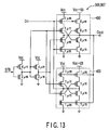
- FIG. 13 shows a configuration of the latch circuit 906 or 907.
- FIG. 14 shows a configuration of the buffer circuit (Buf1) 908 or 909 which drives the gate of the pMOSFET in the transfer gate 904 or 905.
- FIG. 15 shows a configuration of the buffer circuit (Buf0) 910 or 911 which drives the gate of the nMOSFET in the transfer gate 904 or 905. The corresponding gate width is added to each MOSFET in FIGS. 13 to 15.
- the inverters 400 of the first embodiment are connected each other to form a latch circuit.
- the circuit configuration of the buffer 908 or 909 (Buf1) in FIG. 14 and that of the buffer 910 or 911 (Buf0) in FIG. 15 are similar to the configuration of the first embodiment, but differ from the first embodiment in that the first logic circuit differs from the second logic circuit in logic functions. That is, the output switch circuit 110' or 110 switches between the second logic circuit 914 composed of an inverter and the first logic circuit 913 different from an inverter. Either the output switch circuit 110 or 110' may be used.
- the data is stored in the latches 906 and 907 through the transfer gates 904 and 905, respectively, in the operating state.
- the logic amplitude of the output node (Dout) of the flip-flop is 0.5 V determined by Vcc-05, the flip-flop can operate with a low power consumption.
- the gates in the latches 906 and 907 are composed of the inverters 400 (or 400') of the first embodiment, their contents are held with a potential of Vcc or 0. Because the Vcc-05 power supply line of the buffers 908 and 909 driving the transfer gates 904 and 905 is disconnected from the output node Dout in the latch via the off transistor, even if Vcc-05 is brought into the floating state by, for example, the FET 601 as shown in FIG. 9, the data is held without any problem.
- the leakage current in the standby state can be reduced to 100 pA or less.
- the flip-flop When the flip-flop is in active mode, it can realize a logic amplitude of 0.5 V and a low power consumption operation.
- the master-slave flip-flop operates with a low leakage current and a low power consumption. Since the master-slave flip-flop can maintain the low leakage current characteristic in the standby state, regardless of the node potential of Vcc-05, this enables Vcc-05 to be made a floating node.
- the leakage current in the semiconductor integrated circuit can be reduced to only the holding current of the flip-flop as a whole. This enables the power consumption to be reduced remarkably.
- a 100-bit shift register composed of the mater-slave flip-flops was formed experimentally in 0.25- ⁇ m CMOS process. Then, the operation of the shift register was confirmed at 100 MHz.
- FIG. 16 shows another concrete example related to the master-slave flip-flop of FIG. 9.
- Vcc is 1.2 V and Vcc-0.5 is 0.5 V.
- the flop-flop is composed of an inverter 1301 acting as a standby signal buffer, inverters 1302 and 1303 acting as clock buffers, transfer gates 1304, 1305, 1304-1 and 1305-1 made up of pMOSFETs and nMOSFETs, master latch flip-flops 1306 and 1306-1, slave latch flip-flops 1307 and 1307-1, and transfer gate driving buffers 1308 and 1309.
- the corresponding gate width is added to each FET in FIGS. 16 to 19.
- FIG. 17 shows the circuit configuration of the inverter used in each of the master latch flip-flops 1306 and 1306-1 and slave latch flip-flop 1307.
- the circuit configuration of inverter of FIG. 17 is basically the same as that of the FIG. 6 in the first embodiment.
- the inverter of FIG. 17 may take the circuit configuration of FIG. 5.
- FIG. 18 shows the circuit configuration of the transfer gate driving buffer 1308 (Buf1) which drives the gates of the pMOSFETs in the transfer gates 1304 and 1305-1, and the gates of the nMOSFETs in the transfer gates 1305 and 1304-1.
- the standby signal STB is high (or in the standby state)
- a constant voltage of Vcc is outputted to Dout.
- FIG. 19 shows the circuit configuration of the transfer gate driving buffer 1309 (Buf0) which drives the gates of the nMOSFETs in the transfer gates 1304 and 1305-1, and the gates of the pMOSFETs in the transfer gates 1305 and 1304-1.
- the circuit configuration of the buffer 1309 is basically the same as that of FIG. 15 in the second embodiment.
- the FET 1321 is always on, the FET 1321 can be omitted with the source of the FET 300 connected to the Vcc, and since the FET 1322 is always off, the FETs 301 and 1322 can be omitted.
- the data is stored in the master latch flip-flop 1306 and slave latch flip-flop 1307 through the transfer gates 1304 and 1305, respectively.
- the flip-flop can operate with a low power consumption.
- the slave side outputs the potential of Vcc-05, which is a floating node, or the ground potential of 0 V via the flip-flop 1307.
- This master-slave flip-flop enables the leakage current in the standby state to be reduced to 100 pA or less as in the second embodiment.
- the flip-flop When the flip-flop is in active mode, it can realize a logic amplitude of 0.5 V and therefore a low power consumption operation.
- the master-slave flip-flop operates with a low leakage current and a low power consumption. Since the master-slave flip-flop can maintain the low leakage current characteristic in the standby state, regardless of the potential of Vcc-05, this enables Vcc-05 to be made a floating node.
- the leakage current in the semiconductor integrated circuit can be reduced to only the holding current of the flip-flop as a whole. This enables the power consumption to be reduced remarkably.
- a 100-bit shift register composed of the mater-slave flip-flops was formed experimentally in 0.25- ⁇ m CMOS process. Then, the operation of the shift register was confirmed at 100 MHz.
- This invention is not limited to the above embodiments.
- 2-input NAND gates, inverters, and flip-flops, NOR, OR/NAND, AND/NOR, and latch circuits may be used as the logic circuits. Use of these types of circuits would produce the same effect.
- FET switches have been used to bring the internal power supply into the floating state.
- the present invention is not restricted to this method.
- a DC-DC converter may be connected and a logic circuit be added to the gate of the buffer circuit in the final stage of the DC-DC converter, thereby making the output node a floating node.
- all of the FETs have been of the MOS type.
- the FETs of the MOS type here are not limited to FETs using oxide films as gate insulating films and include FETs of the so-called MIS type which use insulating films other than oxide films.
- a semiconductor integrated circuit with logic circuits whose logic amplitude is as low as about 0.5 V comprises a first logic circuit and a second logic circuit.
- the first and second logic circuits have common input terminals and the same logic function.
- the first logic circuit is composed of a circuit block made up of a pMOSFET and a circuit block made up of an nMOSFET, each circuit having a high threshold value.
- the second logic circuit is composed of a circuit block made up of a pMOSFET and a circuit block made up of an nMOSFET, each circuits having a low threshold value.
- An output switch circuit intervenes between the pMOS circuit block and nMOS circuit block in each logic circuit.
- the output switch circuit controls the connection and disconnection of each logic circuit to and from the power supply.
- the second logic circuit using the MOSFET with a low threshold voltage for logical switching is connected to the output, thereby operating the integrated circuit with a low power consumption.
- the first logic circuit with the MOSFET with a high threshold voltage inserted in the leakage current route is connected to the output, thereby enabling the integrated circuit to operate according to the low leakage current characteristic.
- the logic circuits in the operating state, operate from the low potential power supply according to the low power consumption characteristic and, in the standby state, holds the data in the flip-flops and disconnects the other logic circuits from the power supply, thereby remaining in the standby state according to the small leakage current characteristic.
Landscapes
- Physics & Mathematics (AREA)
- Engineering & Computer Science (AREA)
- Computer Hardware Design (AREA)
- Computing Systems (AREA)
- General Engineering & Computer Science (AREA)
- Mathematical Physics (AREA)
- Logic Circuits (AREA)
- Semiconductor Integrated Circuits (AREA)
- Metal-Oxide And Bipolar Metal-Oxide Semiconductor Integrated Circuits (AREA)
Applications Claiming Priority (2)
| Application Number | Priority Date | Filing Date | Title |
|---|---|---|---|
| JP2000395932A JP3548115B2 (ja) | 2000-12-26 | 2000-12-26 | 半導体集積回路及び半導体集積回路装置 |
| JP2000395932 | 2000-12-26 |
Publications (4)
| Publication Number | Publication Date |
|---|---|
| EP1220450A2 true EP1220450A2 (de) | 2002-07-03 |
| EP1220450A3 EP1220450A3 (de) | 2003-07-09 |
| EP1220450B1 EP1220450B1 (de) | 2008-09-10 |
| EP1220450B8 EP1220450B8 (de) | 2008-11-26 |
Family
ID=18861308
Family Applications (1)
| Application Number | Title | Priority Date | Filing Date |
|---|---|---|---|
| EP01310696A Expired - Lifetime EP1220450B8 (de) | 2000-12-26 | 2001-12-20 | Integrierte Halbleiterschaltung |
Country Status (5)
| Country | Link |
|---|---|
| US (1) | US6677797B2 (de) |
| EP (1) | EP1220450B8 (de) |
| JP (1) | JP3548115B2 (de) |
| CN (1) | CN1227740C (de) |
| DE (1) | DE60135728D1 (de) |
Cited By (5)
| Publication number | Priority date | Publication date | Assignee | Title |
|---|---|---|---|---|
| US7180348B2 (en) | 2005-03-24 | 2007-02-20 | Arm Limited | Circuit and method for storing data in operational and sleep modes |
| EP1653314A4 (de) * | 2003-07-28 | 2008-01-30 | Tpo Hong Kong Holding Ltd | Spannungswandlervorrichtung |
| US8390328B2 (en) | 2011-05-13 | 2013-03-05 | Arm Limited | Supplying a clock signal and a gated clock signal to synchronous elements |
| US8879335B2 (en) | 2011-03-31 | 2014-11-04 | Kabushiki Kaisha Toshiba | Input circuit |
| US11437330B2 (en) | 2019-09-03 | 2022-09-06 | Infineon Technologies Ag | Physically obfuscated circuit |
Families Citing this family (22)
| Publication number | Priority date | Publication date | Assignee | Title |
|---|---|---|---|---|
| US6794914B2 (en) * | 2002-05-24 | 2004-09-21 | Qualcomm Incorporated | Non-volatile multi-threshold CMOS latch with leakage control |
| US6850103B2 (en) * | 2002-09-27 | 2005-02-01 | Texas Instruments Incorporated | Low leakage single-step latch circuit |
| JPWO2004054114A1 (ja) * | 2002-12-10 | 2006-04-13 | 株式会社半導体エネルギー研究所 | 半導体装置、デジタル・アナログ変換回路及びそれらを用いた表示装置 |
| US6788125B1 (en) * | 2003-05-28 | 2004-09-07 | Sun Microsystems, Inc. | Stable and accurate CMOS level shifter |
| US6850105B1 (en) | 2003-09-30 | 2005-02-01 | Starcore, Llc | Method and circuitry for preserving a logic state |
| US7183825B2 (en) * | 2004-04-06 | 2007-02-27 | Freescale Semiconductor, Inc. | State retention within a data processing system |
| KR20070034468A (ko) * | 2004-05-14 | 2007-03-28 | 제트모스 테크놀로지 인코포레이티드 | 내부 전압 발생기 구조 및 전력 운영 방법 |
| JP2006050411A (ja) * | 2004-08-06 | 2006-02-16 | Rohm Co Ltd | 半導体装置 |
| US11297705B2 (en) | 2007-10-06 | 2022-04-05 | Lynk Labs, Inc. | Multi-voltage and multi-brightness LED lighting devices and methods of using same |
| US8648539B2 (en) | 2007-10-06 | 2014-02-11 | Lynk Labs, Inc. | Multi-voltage and multi-brightness LED lighting devices and methods of using same |
| JP2012059991A (ja) * | 2010-09-10 | 2012-03-22 | Toshiba Corp | 半導体集積回路 |
| KR20120111284A (ko) * | 2011-03-31 | 2012-10-10 | 에스케이하이닉스 주식회사 | 반도체 장치의 드라이버 회로 및 그 제어 방법 |
| DE102014204287A1 (de) * | 2014-03-07 | 2015-09-10 | Robert Bosch Gmbh | Verfahren zum Betreiben einer Kraftfahrzeugbremseinrichtung sowie Steuergerät für eine Kraftfahrzeugbremseinrichtung |
| US9431353B2 (en) * | 2014-04-09 | 2016-08-30 | Infineon Technologies Ag | Method for manufacturing a digital circuit and digital circuit |
| CN105067988B (zh) * | 2015-07-02 | 2018-03-30 | 英特尔公司 | 集成电路、集成电路测试装置以及方法 |
| WO2018017035A1 (en) * | 2016-07-17 | 2018-01-25 | Hewlett-Packard Development Company, L.P. | Dual rail circuitry using fet pairs |
| US10319362B2 (en) * | 2016-10-27 | 2019-06-11 | Texas Instruments Incorporated | High speed level shifter for high voltage applications |
| CN109768795B (zh) * | 2017-11-09 | 2025-01-17 | 恩智浦美国有限公司 | 低泄漏隔离单元 |
| US10707872B1 (en) * | 2019-03-20 | 2020-07-07 | Semiconductor Components Industries, Llc | Digital buffer circuit |
| CN110310678A (zh) * | 2019-06-04 | 2019-10-08 | 上海新储集成电路有限公司 | 一种智能芯片 |
| CN112786570B (zh) * | 2019-11-01 | 2024-10-22 | 立积电子股份有限公司 | 具有静电放电保护机制的集成电路 |
| CN117275401B (zh) * | 2023-11-03 | 2024-02-27 | 中山市智牛电子有限公司 | 一种图像缩小电路、led显示屏控制卡及图像缩放方法 |
Family Cites Families (5)
| Publication number | Priority date | Publication date | Assignee | Title |
|---|---|---|---|---|
| JP3071612B2 (ja) * | 1993-07-15 | 2000-07-31 | 日本電気株式会社 | Cmos型半導体集積回路 |
| DE19622646B4 (de) | 1995-06-06 | 2005-03-03 | Kabushiki Kaisha Toshiba, Kawasaki | Integrierte Halbleiterschaltungsvorrichtung |
| US5627492A (en) * | 1995-11-03 | 1997-05-06 | Motorola, Inc. | Circuit and method for isolating circuit blocks for reducing power dissipation |
| US5751164A (en) * | 1996-06-24 | 1998-05-12 | Advanced Micro Devices, Inc. | Programmable logic device with multi-level power control |
| JP3195256B2 (ja) | 1996-10-24 | 2001-08-06 | 株式会社東芝 | 半導体集積回路 |
-
2000
- 2000-12-26 JP JP2000395932A patent/JP3548115B2/ja not_active Expired - Fee Related
-
2001
- 2001-12-20 DE DE60135728T patent/DE60135728D1/de not_active Expired - Lifetime
- 2001-12-20 EP EP01310696A patent/EP1220450B8/de not_active Expired - Lifetime
- 2001-12-21 US US10/023,947 patent/US6677797B2/en not_active Expired - Fee Related
- 2001-12-26 CN CN01143922.XA patent/CN1227740C/zh not_active Expired - Fee Related
Cited By (8)
| Publication number | Priority date | Publication date | Assignee | Title |
|---|---|---|---|---|
| EP1653314A4 (de) * | 2003-07-28 | 2008-01-30 | Tpo Hong Kong Holding Ltd | Spannungswandlervorrichtung |
| US7545172B2 (en) | 2003-07-28 | 2009-06-09 | Tpo Hong Kong Holding Limited | Voltage converter apparatus |
| US7180348B2 (en) | 2005-03-24 | 2007-02-20 | Arm Limited | Circuit and method for storing data in operational and sleep modes |
| WO2006100455A3 (en) * | 2005-03-24 | 2007-03-01 | Advanced Risc Mach Ltd | Circuit and method for storing data in operational and sleep modes |
| US7650524B2 (en) | 2005-03-24 | 2010-01-19 | Arm Limited | Circuit and modes for storing data in operational and sleep modes |
| US8879335B2 (en) | 2011-03-31 | 2014-11-04 | Kabushiki Kaisha Toshiba | Input circuit |
| US8390328B2 (en) | 2011-05-13 | 2013-03-05 | Arm Limited | Supplying a clock signal and a gated clock signal to synchronous elements |
| US11437330B2 (en) | 2019-09-03 | 2022-09-06 | Infineon Technologies Ag | Physically obfuscated circuit |
Also Published As
| Publication number | Publication date |
|---|---|
| EP1220450A3 (de) | 2003-07-09 |
| EP1220450B1 (de) | 2008-09-10 |
| EP1220450B8 (de) | 2008-11-26 |
| DE60135728D1 (de) | 2008-10-23 |
| US6677797B2 (en) | 2004-01-13 |
| JP2002198793A (ja) | 2002-07-12 |
| JP3548115B2 (ja) | 2004-07-28 |
| CN1362743A (zh) | 2002-08-07 |
| US20020080663A1 (en) | 2002-06-27 |
| CN1227740C (zh) | 2005-11-16 |
Similar Documents
| Publication | Publication Date | Title |
|---|---|---|
| EP1220450B1 (de) | Integrierte Halbleiterschaltung | |
| EP1537581B1 (de) | Verfahren zur verringerung der stromaufnahme in einer zustandshalteschaltung, zustandshalteschaltung und elektronische einrichtung | |
| US7079413B2 (en) | Semiconductor memory device with back gate potential control circuit for transistor in memory cell | |
| US5144165A (en) | CMOS off-chip driver circuits | |
| US9053975B2 (en) | Semicondutor integrated circuit device and system | |
| US5821769A (en) | Low voltage CMOS logic circuit with threshold voltage control | |
| US20010052623A1 (en) | Semiconductor integrated circuit | |
| US6184716B1 (en) | High voltage output stage for driving an electric load | |
| US20070279082A1 (en) | Semiconductor integrated circuit | |
| US6759873B2 (en) | Reverse biasing logic circuit | |
| US6466054B2 (en) | Level converter circuit | |
| US20040196082A1 (en) | Circuit arrangement | |
| US7183808B2 (en) | Circuit for power management of standard cell application | |
| US7663411B2 (en) | Semiconductor device with a logic circuit | |
| US7902861B2 (en) | Adiabatic CMOS design | |
| US6288586B1 (en) | Circuit for standby current reduction | |
| US7132848B2 (en) | Power management circuit | |
| JP2002135106A (ja) | レベル変換回路及び半導体集積回路 | |
| JP3699878B2 (ja) | 半導体集積回路 | |
| US20250323642A1 (en) | Semiconductor device | |
| US7570106B2 (en) | Substrate voltage generating circuit with improved level shift circuit | |
| CN100414838C (zh) | 标准逻辑工艺上的负电压有效传输电路 | |
| KR101740284B1 (ko) | 전류 구동 능력을 개선한 adcl 인버터 | |
| JP2001060863A (ja) | 半導体集積回路 |
Legal Events
| Date | Code | Title | Description |
|---|---|---|---|
| PUAI | Public reference made under article 153(3) epc to a published international application that has entered the european phase |
Free format text: ORIGINAL CODE: 0009012 |
|
| 17P | Request for examination filed |
Effective date: 20020111 |
|
| AK | Designated contracting states |
Kind code of ref document: A2 Designated state(s): AT BE CH CY DE DK ES FI FR GB GR IE IT LI LU MC NL PT SE TR |
|
| AX | Request for extension of the european patent |
Free format text: AL;LT;LV;MK;RO;SI |
|
| PUAL | Search report despatched |
Free format text: ORIGINAL CODE: 0009013 |
|
| AK | Designated contracting states |
Designated state(s): AT BE CH CY DE DK ES FI FR GB GR IE IT LI LU MC NL PT SE TR |
|
| AX | Request for extension of the european patent |
Extension state: AL LT LV MK RO SI |
|
| RIC1 | Information provided on ipc code assigned before grant |
Ipc: 7H 03K 19/00 A Ipc: 7H 03K 3/012 B Ipc: 7H 03K 19/094 B |
|
| AKX | Designation fees paid |
Designated state(s): DE FR GB |
|
| GRAP | Despatch of communication of intention to grant a patent |
Free format text: ORIGINAL CODE: EPIDOSNIGR1 |
|
| GRAS | Grant fee paid |
Free format text: ORIGINAL CODE: EPIDOSNIGR3 |
|
| GRAA | (expected) grant |
Free format text: ORIGINAL CODE: 0009210 |
|
| AK | Designated contracting states |
Kind code of ref document: B1 Designated state(s): DE FR GB |
|
| REG | Reference to a national code |
Ref country code: GB Ref legal event code: FG4D |
|
| REF | Corresponds to: |
Ref document number: 60135728 Country of ref document: DE Date of ref document: 20081023 Kind code of ref document: P |
|
| RIN2 | Information on inventor provided after grant (corrected) |
Inventor name: KAMEYAMA, ATSUSHI,C Inventor name: YOSHIDA, MASAKOC Inventor name: OHUCHI, KAZUNORI,C Inventor name: FUSE, TSUNEAKI,C |
|
| PLBE | No opposition filed within time limit |
Free format text: ORIGINAL CODE: 0009261 |
|
| STAA | Information on the status of an ep patent application or granted ep patent |
Free format text: STATUS: NO OPPOSITION FILED WITHIN TIME LIMIT |
|
| 26N | No opposition filed |
Effective date: 20090611 |
|
| PGFP | Annual fee paid to national office [announced via postgrant information from national office to epo] |
Ref country code: FR Payment date: 20091221 Year of fee payment: 9 Ref country code: GB Payment date: 20091216 Year of fee payment: 9 |
|
| PGFP | Annual fee paid to national office [announced via postgrant information from national office to epo] |
Ref country code: DE Payment date: 20091217 Year of fee payment: 9 |
|
| GBPC | Gb: european patent ceased through non-payment of renewal fee |
Effective date: 20101220 |
|
| REG | Reference to a national code |
Ref country code: FR Ref legal event code: ST Effective date: 20110831 |
|
| PG25 | Lapsed in a contracting state [announced via postgrant information from national office to epo] |
Ref country code: FR Free format text: LAPSE BECAUSE OF NON-PAYMENT OF DUE FEES Effective date: 20110103 |
|
| REG | Reference to a national code |
Ref country code: DE Ref legal event code: R119 Ref document number: 60135728 Country of ref document: DE Effective date: 20110701 |
|
| PG25 | Lapsed in a contracting state [announced via postgrant information from national office to epo] |
Ref country code: DE Free format text: LAPSE BECAUSE OF NON-PAYMENT OF DUE FEES Effective date: 20110701 Ref country code: GB Free format text: LAPSE BECAUSE OF NON-PAYMENT OF DUE FEES Effective date: 20101220 |