EP1221582A2 - Dispositif opto-électronique - Google Patents
Dispositif opto-électronique Download PDFInfo
- Publication number
- EP1221582A2 EP1221582A2 EP01130581A EP01130581A EP1221582A2 EP 1221582 A2 EP1221582 A2 EP 1221582A2 EP 01130581 A EP01130581 A EP 01130581A EP 01130581 A EP01130581 A EP 01130581A EP 1221582 A2 EP1221582 A2 EP 1221582A2
- Authority
- EP
- European Patent Office
- Prior art keywords
- optoelectronic device
- frame
- transmitter
- light beams
- transmitted light
- Prior art date
- Legal status (The legal status is an assumption and is not a legal conclusion. Google has not performed a legal analysis and makes no representation as to the accuracy of the status listed.)
- Granted
Links
- 230000005693 optoelectronics Effects 0.000 title claims description 33
- 238000011156 evaluation Methods 0.000 claims abstract description 20
- 230000005284 excitation Effects 0.000 claims description 12
- 238000005259 measurement Methods 0.000 claims description 11
- 238000000034 method Methods 0.000 claims description 3
- 238000002366 time-of-flight method Methods 0.000 claims description 3
- XAGFODPZIPBFFR-UHFFFAOYSA-N aluminium Chemical compound [Al] XAGFODPZIPBFFR-UHFFFAOYSA-N 0.000 claims description 2
- 229910052782 aluminium Inorganic materials 0.000 claims description 2
- 229910021419 crystalline silicon Inorganic materials 0.000 claims description 2
- 238000005070 sampling Methods 0.000 description 5
- 230000005540 biological transmission Effects 0.000 description 4
- 238000001514 detection method Methods 0.000 description 3
- 238000010586 diagram Methods 0.000 description 2
- 230000003287 optical effect Effects 0.000 description 2
- 230000000737 periodic effect Effects 0.000 description 2
- 230000015572 biosynthetic process Effects 0.000 description 1
- 230000000295 complement effect Effects 0.000 description 1
- 238000013461 design Methods 0.000 description 1
- 238000011161 development Methods 0.000 description 1
- 230000018109 developmental process Effects 0.000 description 1
- ZINJLDJMHCUBIP-UHFFFAOYSA-N ethametsulfuron-methyl Chemical compound CCOC1=NC(NC)=NC(NC(=O)NS(=O)(=O)C=2C(=CC=CC=2)C(=O)OC)=N1 ZINJLDJMHCUBIP-UHFFFAOYSA-N 0.000 description 1
- 238000000691 measurement method Methods 0.000 description 1
- 238000007493 shaping process Methods 0.000 description 1
- 230000001360 synchronised effect Effects 0.000 description 1
Images

Classifications
-
- G—PHYSICS
- G01—MEASURING; TESTING
- G01S—RADIO DIRECTION-FINDING; RADIO NAVIGATION; DETERMINING DISTANCE OR VELOCITY BY USE OF RADIO WAVES; LOCATING OR PRESENCE-DETECTING BY USE OF THE REFLECTION OR RERADIATION OF RADIO WAVES; ANALOGOUS ARRANGEMENTS USING OTHER WAVES
- G01S7/00—Details of systems according to groups G01S13/00, G01S15/00, G01S17/00
- G01S7/48—Details of systems according to groups G01S13/00, G01S15/00, G01S17/00 of systems according to group G01S17/00
- G01S7/481—Constructional features, e.g. arrangements of optical elements
- G01S7/4817—Constructional features, e.g. arrangements of optical elements relating to scanning
-
- G—PHYSICS
- G01—MEASURING; TESTING
- G01S—RADIO DIRECTION-FINDING; RADIO NAVIGATION; DETERMINING DISTANCE OR VELOCITY BY USE OF RADIO WAVES; LOCATING OR PRESENCE-DETECTING BY USE OF THE REFLECTION OR RERADIATION OF RADIO WAVES; ANALOGOUS ARRANGEMENTS USING OTHER WAVES
- G01S17/00—Systems using the reflection or reradiation of electromagnetic waves other than radio waves, e.g. lidar systems
- G01S17/02—Systems using the reflection of electromagnetic waves other than radio waves
-
- G—PHYSICS
- G02—OPTICS
- G02B—OPTICAL ELEMENTS, SYSTEMS OR APPARATUS
- G02B7/00—Mountings, adjusting means, or light-tight connections, for optical elements
- G02B7/28—Systems for automatic generation of focusing signals
- G02B7/30—Systems for automatic generation of focusing signals using parallactic triangle with a base line
- G02B7/32—Systems for automatic generation of focusing signals using parallactic triangle with a base line using active means, e.g. light emitter
Definitions
- the invention relates to an optoelectronic device according to the preamble of claim 1.
- Such a device is known from DE 198 21 974 A1.
- the device is designed as a so-called 3D distance camera and has one Transmitter with which a surface of an object to be detected is flat is illuminated.
- the receiver of the 3D distance image camera consists of a flat arrangement of receiving elements, by means of which a distance measurement is carried out. The distance measurement takes place after the Phase measurement principle.
- the transmitted light emitted by the transmitter is with a predetermined one Phase amplitude modulated.
- the phase differences determined in this way offer a measure of the respective object distance.
- the receiving elements are designed as so-called photo mixer detectors, by means of which one accurate distance measurement is possible even when the object surface Contrast fluctuations in the form of light-dark borders.
- the single ones Photo mixer detectors are controlled with the modulation clock of the transmitter, whereby the reception light pixel by pixel for the individual reception elements is demodulated so that according to the phase measurement method the respective distance can be determined.
- Another 3D distance camera is known from DE 197 57 595 C2. in the The difference to the subject of DE 198 21 974 A1 is with this 3D distance camera a receiver is provided, the receiving elements as CMOS elements are formed, by means of which by the time-of-flight method a distance determination is carried out.
- a disadvantage of these devices is that the area lighting the object surface requires a large light output of the transmitter in order to to ensure the required power density on the object.
- a laser must be used for the distance measurement as a transmitter and since this to achieve the required power density on the object surface Such devices have to be operated at high power the problem of eye safety. To meet the requirements For an eye-safe mode of operation, the laser must have a power of approx 1mW can be limited.
- the Power of the reception light with the square of the distance With diffuse reflection of the reception light on the object surface, the Power of the reception light with the square of the distance. by virtue of The limited transmission power of the transmitter can therefore only be used in extreme objects short distances can be reliably detected.
- the invention has for its object an optoelectronic device of the type mentioned at the outset in such a way that objects can be quickly and safely in particular, can also be detected at a greater distance.
- the optoelectronic device is used to determine Distance profiles of objects and has a light beam emitting Transmitter, receiving a received light beam from a flat arrangement receiver consisting of receiving elements and an evaluation unit for the evaluation of reception signals generated in the reception elements on. Only the transmitted light rays are over an oscillating mirror periodically deflected in two spatial directions so that this is on the surface of the object over a scanning area. The transmitted light rays reflected on the object are guided to the receiver as reception light beams.
- the optoelectronic device represents a 3D distance camera
- An essential advantage of the 3D distance camera according to the invention is that an object surface is not illuminated areal is, but periodically scanned by means of the transmitted light beams becomes.
- the beam diameter of the transmitted light beams is considerably smaller than the object surface to be scanned.
- the one pictured on the receiver Transmitted light spot of the transmitted light beams is considerably smaller than the area of the recipient consisting of the receiving elements.
- the object surface can be scanned by means of the transmitted light beams Power density of the transmitted light on the object surface compared to Systems that operate with planar transmission lights are significantly increased, without violating the eye safety requirements.
- the deflection of the oscillating mirror with the reading process of the receiving elements of the Receiver synchronized in such a way that only the receive signals of those Receiving elements are read into the evaluation unit, which in the area the received light beams incident on the receiver and their Neighbor cells are.
- the reception signals of the other reception elements are not evaluated.
- the level of a previous one Sampling are below a predetermined threshold.
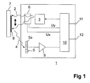
- FIG. 1 shows the block diagram of an exemplary embodiment of the optoelectronic device 1 according to the invention.
- the optoelectronic device 1 is designed as a 3D distance camera and has a transmitter 3 emitting light rays 2 and a receiver 5 receiving light rays 4.
- the transmitter 3 is formed by a laser diode.
- the receiver 5 consists of a flat arrangement of receiving elements 5a.
- the receiving elements 5a are preferably of identical design and are arranged lying in one plane.
- the photosensitive surfaces of the receiving elements 5a preferably complement one another to form a square receiver surface.
- the transmitted light beams 2 are periodically deflected in two spatial directions by an oscillating mirror 6, so that the transmitted light beams 2 sweep over a scanning surface 8 on the object 7 to be detected.
- the received light rays 4 reflected by the object 7 are not guided over the oscillating mirror 6 and reach the receiver 5 directly.
- a control unit (not shown) is integrated in the oscillating mirror 6. In this control voltage U x , U y are generated, by means of which the transmitted light beams 2 are deflected in two spatial directions x and y.
- the received signals at the outputs of the receiving elements 5a are amplified in an amplifier 9 and then passed to an evaluation unit 10, which is preferably formed by a microprocessor.
- the transmitter 3 and the receiving elements 5a form Distance sensors working according to the time-of-flight method.
- the distance measurement can be based on the phase measurement principle.
- the receiving elements 5a for example, designed as a photonic mixer device such as the one shown in FIG are described in DE 198 21 974 A1.
- the transmitter 3 emitted transmission light beams 2 by means of a modulation unit, not shown an amplitude modulation is impressed.
- the evaluation unit 10 the phase difference between the transmitted light beams emitted by the transmitter 3 2 and that reflected back from object 7 to the respective receiving element 5a Receiving light rays 4 calculated.
- the distance measurement can be carried out using the pulse transit time method respectively.
- the transmitter emits 3 transmitted light beams 2 in Form of predetermined sequences of transmitted light pulses.
- the evaluation unit 10 is used to determine the distance, the transit time of the transmitter 3 and as received light pulses back to the receiver 5 reflected light pulses determined.
- the receiving elements 5a are special formed as CMOS elements, as described in DE 197 57 595 C2 are.
- the distance profile of an object surface determined in the evaluation unit 10 is via an interface unit 11, which forms a serial interface and is also connected to the evaluation unit 10.
- an interface unit 11 which forms a serial interface and is also connected to the evaluation unit 10.
- parameter input 12 parameter values can be entered.
- a threshold value can be entered as a parameter value, with which the received signals of the receiving elements 5a are evaluated.
- Threshold value evaluation of the receiving elements 5a are carried out within one sampling period the unexposed receiving elements 5a are detected. During the following sampling period are then only the receiving elements 5a that were previously were exposed, and their neighboring elements were used for evaluation. By including the neighboring elements in the evaluation, In the case of an object movement between two scanning periods, a safe one Obtain object detection. Through this data reduction, the dynamic of the 3D distance camera can be increased significantly. Was during a or If no object is recognized for several sampling periods, the first sampling period in which an object is registered again, initially the entire recipient area evaluated. In the subsequent object detections then the mentioned data reduction again.
- data can also be reduced in such a way that the reading out of reception signals of the various reception elements 5a is coupled to the deflection movement of the oscillating mirror 6.
- the Factor exploited that depending on the current position of the oscillating mirror 6 Receiving light rays 4 reflected back from the object 7 only to certain ones Impact areas of the receiver 5. For each current angular position of the Oscillating mirror 6 then only the received signals of those receiving elements 5a read out in the exposed areas of the receiver 5 lie.
- FIG. 2 shows the optical components of the optoelectronic device 1 according to Figure 1.
- the transmitter 3 is a collimator 13 for beam shaping Subordinate light beams 2.
- the collimated transmission light beams 2 are deflected by the oscillating mirror 6 in two spatial directions, the Angular range in each spatial direction, which is different from that on the oscillating mirror 6 deflected transmitted light beams 2 is swept, in the range between 5 ° and is 20 ° and is preferably 10 °.
- Receiving light beams 4 are reflected by receiving optics 14 mapped the receiver 5.
- FIG. 3 shows a detailed representation of the oscillating mirror 6.
- the oscillating mirror 6 is designed as a micromechanical scanner mirror, which is a plate-shaped Has mirror element 15, on which the transmitted light beams 2nd be reflected.
- the mirror element 15 consists of a single-crystalline silicon plate, which is coated with an aluminum layer. This forms the Mirror surface on which the transmitted light beams 2 are reflected.
- the mirror element 15 is fastened to a first frame 17 by means of two first torsion bars 16.
- the torsion bars 16 open out on opposite side walls of the mirror element 15 and run along a first axis of rotation D x .
- the mirror element 15 is rotatably supported in the first frame 17 with respect to the axis of rotation D x by torsion of the torsion bars 16.
- the first frame 17 lies within a second frame 18.
- the two frames 17, 18 are connected via second torsion bars 19 which run in a second axis of rotation D y .
- second torsion bars 19 By torsion of the second torsion bars 19, the first frame 17 with the mirror element 15 is rotatably supported in the second frame 18 with respect to the axis of rotation D y .
- the plate-shaped mirror element 15 has a square cross section on.
- the first and second frames 17, 18 have square contours and are arranged concentrically to the mirror element 15.
- First drive electrodes 20 are provided in the wall segments of the first frame 17 which run parallel to the first axis of rotation D x .
- control voltages U x with a predetermined excitation frequency f x , the mirror element 15 is rotated with the corresponding excitation frequency f x with respect to the axis of rotation D x .
- Second drive electrodes 21 are provided in the wall segments of the second frame 18 that run parallel to the second axis of rotation D y .
- the spatial course of the scanning of the scanning surface 8 can be adjusted.
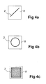
- FIGS. 4a-c show different scanning lines on a scanning surface 8 of an object 7, which is deflected by means of the oscillating mirror 6 Transmitting light beams 2 are generated.
- Figure 4a shows a scan line in the form of a straight line. This pattern of a scanning line is obtained by excitation frequencies f x , f y of the same size.
- Figure 4b shows a circular scan line
- the beam spot of the transmitted light beams runs 2 in the plane of the scanning surface 8 along scanning lines, which form a Portugal pattern.
- this Lisbon pattern can be specified in a targeted manner.
- n ABS (1 / (p-1))
- ABS stands for the formation of the absolute reference.
- the image frequency f b that is to say the speeds of the scanning of the scanning surface 8, can also be set in accordance with the following relationship. f b ⁇ f x / n
- the image frequency f b is proportional to the excitation frequency f x (and also f y ) and inversely proportional to the number n of scanning lines per scanning area 8.
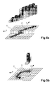
- FIG. 5a shows a first application example of the optoelectronic device 1.
- the object 7 has two flat partial surfaces, which are separated by an edge are separated.
- the transmitted light beams 2 become straight running scan line periodically.
- the diagonal line as the transmitted light pattern is placed so that the one to be detected Edge is cut as crosswise as possible.
- the cell grid of the receiving elements 5a of the receiver 5 onto the object 7 projected and the received signal levels of the receiving elements 5a as Bar graphs plotted. Only the cells shown toned in Figure 5a deliver receive signals that exceed the threshold. Only that Received signals of these receiving elements 5a are in the evaluation unit 10 read in and evaluated there. This shows that the Evaluation can be limited to a few receiving elements 5a and still provides a precise statement about the edge structure of the object 7.
- Figure 5b shows a second application example in which the transmitted light beams 2 are guided along a circular scan line.
Landscapes
- Physics & Mathematics (AREA)
- Engineering & Computer Science (AREA)
- General Physics & Mathematics (AREA)
- Computer Networks & Wireless Communication (AREA)
- Radar, Positioning & Navigation (AREA)
- Remote Sensing (AREA)
- Electromagnetism (AREA)
- Optics & Photonics (AREA)
- Optical Radar Systems And Details Thereof (AREA)
- Measurement Of Optical Distance (AREA)
Applications Claiming Priority (2)
| Application Number | Priority Date | Filing Date | Title |
|---|---|---|---|
| DE10100353 | 2001-01-05 | ||
| DE10100353 | 2001-01-05 |
Publications (3)
| Publication Number | Publication Date |
|---|---|
| EP1221582A2 true EP1221582A2 (fr) | 2002-07-10 |
| EP1221582A3 EP1221582A3 (fr) | 2004-12-29 |
| EP1221582B1 EP1221582B1 (fr) | 2013-03-13 |
Family
ID=7669852
Family Applications (1)
| Application Number | Title | Priority Date | Filing Date |
|---|---|---|---|
| EP01130581A Expired - Lifetime EP1221582B1 (fr) | 2001-01-05 | 2001-12-21 | Dispositif opto-électronique |
Country Status (1)
| Country | Link |
|---|---|
| EP (1) | EP1221582B1 (fr) |
Cited By (13)
| Publication number | Priority date | Publication date | Assignee | Title |
|---|---|---|---|---|
| EP1515161A1 (fr) * | 2003-09-15 | 2005-03-16 | Deere & Company | Télémètre et procédé correspondant |
| EP1632790A3 (fr) * | 2003-09-15 | 2006-03-15 | Deere & Company | Télémètre et procédé pour déterminer la distance entre an objet et un point de référence |
| DE102004008925B4 (de) * | 2003-02-28 | 2006-04-13 | Leuze Electronic Gmbh & Co Kg | Optoelektronische Vorrichtung |
| WO2008018955A3 (fr) * | 2006-06-27 | 2008-09-25 | Arete Associates | Configuration de lidar de type caméra |
| WO2011002755A1 (fr) * | 2009-07-02 | 2011-01-06 | Robert Bosch Gmbh | Procédé et appareil pour obtenir des données tridimensionnelles avec un dispositif portable |
| US7916898B2 (en) | 2003-09-15 | 2011-03-29 | Deere & Company | Method and system for identifying an edge of a crop |
| DE102010005993A1 (de) * | 2010-01-27 | 2011-07-28 | Deutsches Zentrum für Luft- und Raumfahrt e.V., 51147 | Laserscanner-Einrichtung und Verfahren zur dreidimensionalen berührungslosen Umgebungserfassung mit einer Laserscanner-Einrichtung |
| WO2011002771A3 (fr) * | 2009-07-02 | 2012-07-19 | Robert Bosch Gmbh | Système et procédé tridimensionnels de perception pour plateforme mobile |
| TWI385474B (zh) * | 2008-05-02 | 2013-02-11 | Hon Hai Prec Ind Co Ltd | 攝像裝置及攝像方法 |
| US8958057B2 (en) | 2006-06-27 | 2015-02-17 | Arete Associates | Camera-style lidar setup |
| WO2015189025A1 (fr) * | 2014-06-11 | 2015-12-17 | Robert Bosch Gmbh | Système de lidar de véhicule |
| EP3238435A4 (fr) * | 2014-12-22 | 2018-07-18 | Google LLC | Illuminateur pour système de caméra ayant une capture temps de vol en trois dimensions avec élément miroir mobile |
| DE102017212384A1 (de) * | 2017-07-19 | 2019-01-24 | Myestro Interactive Gmbh | Ablenkeinrichtung für einen Laserstrahl |
Citations (4)
| Publication number | Priority date | Publication date | Assignee | Title |
|---|---|---|---|---|
| US5418608A (en) | 1993-05-04 | 1995-05-23 | Harbor Branch Oceanographic Institution Inc. | Three dimensional mapping systems and methods |
| US5760886A (en) | 1994-07-29 | 1998-06-02 | Miyazaki; Hidenori | Scanning-type distance measurement device responsive to selected signals |
| DE19821974A1 (de) | 1998-05-18 | 1999-11-25 | Rudolf Schwarte | Vorrichtung und Verfahren zur Erfassung von Phase und Amplitude elektromagnetischer Wellen |
| DE19757595C2 (de) | 1997-12-23 | 2000-05-11 | Siemens Ag | Verfahren und Vorrichtung zur Aufnahme eines dreidimensionalen Abstandsbildes |
Family Cites Families (6)
| Publication number | Priority date | Publication date | Assignee | Title |
|---|---|---|---|---|
| DE3543648A1 (de) * | 1985-12-11 | 1987-06-19 | Hipp Johann F | Verfahren und einrichtung zur systematischen ablenkung von licht |
| US4896343A (en) * | 1988-05-02 | 1990-01-23 | Saunders Allan M | Radiation apparatus with distance mapper for dose control |
| US5872880A (en) * | 1996-08-12 | 1999-02-16 | Ronald S. Maynard | Hybrid-optical multi-axis beam steering apparatus |
| DE19833207A1 (de) * | 1998-07-23 | 2000-02-17 | Siemens Ag | Verfahren und Vorrichtung zur Aufnahme eines dreidimensionalen Abstandsbildes |
| US6122039A (en) * | 1998-10-28 | 2000-09-19 | Banner Engineering Corp. | Method and apparatus to detect and report object displacement utilizing optical triangulation principles |
| EP1037069A3 (fr) * | 1999-03-17 | 2004-01-14 | Matsushita Electric Industrial Co., Ltd. | Télémètre |
-
2001
- 2001-12-21 EP EP01130581A patent/EP1221582B1/fr not_active Expired - Lifetime
Patent Citations (4)
| Publication number | Priority date | Publication date | Assignee | Title |
|---|---|---|---|---|
| US5418608A (en) | 1993-05-04 | 1995-05-23 | Harbor Branch Oceanographic Institution Inc. | Three dimensional mapping systems and methods |
| US5760886A (en) | 1994-07-29 | 1998-06-02 | Miyazaki; Hidenori | Scanning-type distance measurement device responsive to selected signals |
| DE19757595C2 (de) | 1997-12-23 | 2000-05-11 | Siemens Ag | Verfahren und Vorrichtung zur Aufnahme eines dreidimensionalen Abstandsbildes |
| DE19821974A1 (de) | 1998-05-18 | 1999-11-25 | Rudolf Schwarte | Vorrichtung und Verfahren zur Erfassung von Phase und Amplitude elektromagnetischer Wellen |
Cited By (19)
| Publication number | Priority date | Publication date | Assignee | Title |
|---|---|---|---|---|
| DE102004008925B4 (de) * | 2003-02-28 | 2006-04-13 | Leuze Electronic Gmbh & Co Kg | Optoelektronische Vorrichtung |
| US7916898B2 (en) | 2003-09-15 | 2011-03-29 | Deere & Company | Method and system for identifying an edge of a crop |
| EP1632790A3 (fr) * | 2003-09-15 | 2006-03-15 | Deere & Company | Télémètre et procédé pour déterminer la distance entre an objet et un point de référence |
| US7064810B2 (en) | 2003-09-15 | 2006-06-20 | Deere & Company | Optical range finder with directed attention |
| US7206063B2 (en) | 2003-09-15 | 2007-04-17 | Deere & Company | Optical range finder with directed attention |
| EP1515161A1 (fr) * | 2003-09-15 | 2005-03-16 | Deere & Company | Télémètre et procédé correspondant |
| US8958057B2 (en) | 2006-06-27 | 2015-02-17 | Arete Associates | Camera-style lidar setup |
| WO2008018955A3 (fr) * | 2006-06-27 | 2008-09-25 | Arete Associates | Configuration de lidar de type caméra |
| TWI385474B (zh) * | 2008-05-02 | 2013-02-11 | Hon Hai Prec Ind Co Ltd | 攝像裝置及攝像方法 |
| WO2011002755A1 (fr) * | 2009-07-02 | 2011-01-06 | Robert Bosch Gmbh | Procédé et appareil pour obtenir des données tridimensionnelles avec un dispositif portable |
| WO2011002771A3 (fr) * | 2009-07-02 | 2012-07-19 | Robert Bosch Gmbh | Système et procédé tridimensionnels de perception pour plateforme mobile |
| US8274507B2 (en) | 2009-07-02 | 2012-09-25 | Robert Bosch Gmbh | Method and apparatus for obtaining 3-dimensional data with a portable device |
| DE102010005993A1 (de) * | 2010-01-27 | 2011-07-28 | Deutsches Zentrum für Luft- und Raumfahrt e.V., 51147 | Laserscanner-Einrichtung und Verfahren zur dreidimensionalen berührungslosen Umgebungserfassung mit einer Laserscanner-Einrichtung |
| US8963997B2 (en) | 2010-01-27 | 2015-02-24 | Deutsches Zentrum Fuer Luft-Und Raumfahrt E.V. | Laser scanner device and method for three-dimensional contactless recording of the surrounding area by means of a laser scanner device |
| DE102010005993B4 (de) * | 2010-01-27 | 2016-10-20 | Deutsches Zentrum für Luft- und Raumfahrt e.V. | Laserscanner-Einrichtung und Verfahren zur dreidimensionalen berührungslosen Umgebungserfassung mit einer Laserscanner-Einrichtung |
| WO2015189025A1 (fr) * | 2014-06-11 | 2015-12-17 | Robert Bosch Gmbh | Système de lidar de véhicule |
| EP3238435A4 (fr) * | 2014-12-22 | 2018-07-18 | Google LLC | Illuminateur pour système de caméra ayant une capture temps de vol en trois dimensions avec élément miroir mobile |
| US10306209B2 (en) | 2014-12-22 | 2019-05-28 | Google Llc | Illuminator for camera system having three dimensional time-of-flight capture with movable mirror element |
| DE102017212384A1 (de) * | 2017-07-19 | 2019-01-24 | Myestro Interactive Gmbh | Ablenkeinrichtung für einen Laserstrahl |
Also Published As
| Publication number | Publication date |
|---|---|
| EP1221582A3 (fr) | 2004-12-29 |
| EP1221582B1 (fr) | 2013-03-13 |
Similar Documents
| Publication | Publication Date | Title |
|---|---|---|
| DE2256736C3 (de) | Meßanordnung zur automatischen Prüfung der Oberflächenbeschaffenheit und Ebenheit einer Werkstückoberfläche | |
| DE10146752B4 (de) | Optoelektronische Vorrichtung | |
| EP1300715B1 (fr) | Dispositif de détection optoélectronique | |
| DE19531632B4 (de) | Entfernungsmeßgerät | |
| EP1221582B1 (fr) | Dispositif opto-électronique | |
| DE19936847A1 (de) | Abstandsmeßvorrichtung | |
| DE112017000127T5 (de) | 2D Lidar-Scannen mit hoher Präzision mit einem drehbaren konkaven Spiegel und einer Strahllenkvorrichtung | |
| DE4341080C1 (de) | Lichtelektrische Vorrichtung mit einem Testobjekt | |
| WO2003002939A1 (fr) | Dispositif de mesure optique de distance sur une plage de mesure etendue | |
| DE102015200224A1 (de) | 3D-LIDAR-Sensor | |
| DE10355620A1 (de) | Fahrzeugradarvorrichtung | |
| EP3032275B1 (fr) | Capteur optoelectronique et procede destine a la saisie d'objets | |
| EP1176430B1 (fr) | Dispositif optoélectronique | |
| DE3036257A1 (de) | Vorrichtung zur elektro-optischen abstandsmessung | |
| DE102007028062B4 (de) | Radarvorrichtung | |
| EP3193195B1 (fr) | Capteur optique | |
| DE102017116597A1 (de) | Sendevorrichtung für ein abtastendes optisches Detektionssystem eines Fahrzeugs, Detektionssystem, Fahrerassistenzsystem, Verfahren zur Steuerung einer Strahlrichtung eines optischen Sendesignals | |
| DE102017223658B4 (de) | LIDAR-Vorrichtung (100) zur Erfassung eines Objekts | |
| EP1921565B1 (fr) | Appareil de lecture d'un code à barres | |
| EP0230892A2 (fr) | Dispositif optique de balayage par une roue à miroir | |
| EP3070496A1 (fr) | Dispositif de balayage a polygone et procede de detection d'objets | |
| DE2800351B2 (de) | Optische Vorrichtung zur Bestimmung des Lichtaustrittswinkels bei einer mit einem Lichtfleck abgetasteten Materialbahn | |
| DE4029259A1 (de) | Optisches abtastsystem | |
| EP1279005A1 (fr) | Unite de balayage pour dispositif de mesure optique de la position | |
| EP1134545A1 (fr) | Capteur de distance |
Legal Events
| Date | Code | Title | Description |
|---|---|---|---|
| PUAI | Public reference made under article 153(3) epc to a published international application that has entered the european phase |
Free format text: ORIGINAL CODE: 0009012 |
|
| 17P | Request for examination filed |
Effective date: 20020118 |
|
| AK | Designated contracting states |
Kind code of ref document: A2 Designated state(s): AT BE CH CY DE DK ES FI FR GB GR IE IT LI LU MC NL PT SE TR |
|
| AX | Request for extension of the european patent |
Free format text: AL;LT;LV;MK;RO;SI |
|
| PUAL | Search report despatched |
Free format text: ORIGINAL CODE: 0009013 |
|
| AK | Designated contracting states |
Kind code of ref document: A3 Designated state(s): AT BE CH CY DE DK ES FI FR GB GR IE IT LI LU MC NL PT SE TR |
|
| AX | Request for extension of the european patent |
Extension state: AL LT LV MK RO SI |
|
| RIC1 | Information provided on ipc code assigned before grant |
Ipc: 7G 01B 11/02 A Ipc: 7G 01S 7/481 B Ipc: 7G 01B 7/02 B |
|
| 17Q | First examination report despatched |
Effective date: 20050208 |
|
| AKX | Designation fees paid |
Designated state(s): AT BE CH CY DE DK ES FI FR GB GR IE IT LI LU MC NL PT SE TR |
|
| REG | Reference to a national code |
Ref country code: DE Ref legal event code: R079 Ref document number: 50116256 Country of ref document: DE Free format text: PREVIOUS MAIN CLASS: G01B0011020000 Ipc: G02B0007320000 |
|
| GRAP | Despatch of communication of intention to grant a patent |
Free format text: ORIGINAL CODE: EPIDOSNIGR1 |
|
| RIC1 | Information provided on ipc code assigned before grant |
Ipc: G01S 17/02 20060101ALI20121009BHEP Ipc: G01S 7/481 20060101ALI20121009BHEP Ipc: G02B 7/32 20060101AFI20121009BHEP |
|
| GRAS | Grant fee paid |
Free format text: ORIGINAL CODE: EPIDOSNIGR3 |
|
| GRAA | (expected) grant |
Free format text: ORIGINAL CODE: 0009210 |
|
| RAP1 | Party data changed (applicant data changed or rights of an application transferred) |
Owner name: LEUZE ELECTRONIC GMBH + CO. KG |
|
| RBV | Designated contracting states (corrected) |
Designated state(s): DE |
|
| AK | Designated contracting states |
Kind code of ref document: B1 Designated state(s): DE |
|
| REG | Reference to a national code |
Ref country code: DE Ref legal event code: R096 Ref document number: 50116256 Country of ref document: DE Effective date: 20130508 |
|
| PLBE | No opposition filed within time limit |
Free format text: ORIGINAL CODE: 0009261 |
|
| STAA | Information on the status of an ep patent application or granted ep patent |
Free format text: STATUS: NO OPPOSITION FILED WITHIN TIME LIMIT |
|
| 26N | No opposition filed |
Effective date: 20131216 |
|
| REG | Reference to a national code |
Ref country code: DE Ref legal event code: R097 Ref document number: 50116256 Country of ref document: DE Effective date: 20131216 |
|
| PGFP | Annual fee paid to national office [announced via postgrant information from national office to epo] |
Ref country code: DE Payment date: 20181213 Year of fee payment: 18 |
|
| REG | Reference to a national code |
Ref country code: DE Ref legal event code: R119 Ref document number: 50116256 Country of ref document: DE |
|
| PG25 | Lapsed in a contracting state [announced via postgrant information from national office to epo] |
Ref country code: DE Free format text: LAPSE BECAUSE OF NON-PAYMENT OF DUE FEES Effective date: 20200701 |