EP1223421A2 - Lecteur de biopuce - Google Patents
Lecteur de biopuce Download PDFInfo
- Publication number
- EP1223421A2 EP1223421A2 EP01120597A EP01120597A EP1223421A2 EP 1223421 A2 EP1223421 A2 EP 1223421A2 EP 01120597 A EP01120597 A EP 01120597A EP 01120597 A EP01120597 A EP 01120597A EP 1223421 A2 EP1223421 A2 EP 1223421A2
- Authority
- EP
- European Patent Office
- Prior art keywords
- biochip
- light
- samples
- image
- biochip reader
- Prior art date
- Legal status (The legal status is an assumption and is not a legal conclusion. Google has not performed a legal analysis and makes no representation as to the accuracy of the status listed.)
- Granted
Links
Images



Classifications
-
- G—PHYSICS
- G01—MEASURING; TESTING
- G01N—INVESTIGATING OR ANALYSING MATERIALS BY DETERMINING THEIR CHEMICAL OR PHYSICAL PROPERTIES
- G01N21/00—Investigating or analysing materials by the use of optical means, i.e. using sub-millimetre waves, infrared, visible or ultraviolet light
- G01N21/62—Systems in which the material investigated is excited whereby it emits light or causes a change in wavelength of the incident light
- G01N21/63—Systems in which the material investigated is excited whereby it emits light or causes a change in wavelength of the incident light optically excited
- G01N21/64—Fluorescence; Phosphorescence
- G01N21/645—Specially adapted constructive features of fluorimeters
- G01N21/6452—Individual samples arranged in a regular 2D-array, e.g. multiwell plates
-
- G—PHYSICS
- G01—MEASURING; TESTING
- G01N—INVESTIGATING OR ANALYSING MATERIALS BY DETERMINING THEIR CHEMICAL OR PHYSICAL PROPERTIES
- G01N21/00—Investigating or analysing materials by the use of optical means, i.e. using sub-millimetre waves, infrared, visible or ultraviolet light
- G01N21/62—Systems in which the material investigated is excited whereby it emits light or causes a change in wavelength of the incident light
- G01N21/63—Systems in which the material investigated is excited whereby it emits light or causes a change in wavelength of the incident light optically excited
- G01N21/64—Fluorescence; Phosphorescence
- G01N21/6428—Measuring fluorescence of fluorescent products of reactions or of fluorochrome labelled reactive substances, e.g. measuring quenching effects, using measuring "optrodes"
-
- B—PERFORMING OPERATIONS; TRANSPORTING
- B01—PHYSICAL OR CHEMICAL PROCESSES OR APPARATUS IN GENERAL
- B01J—CHEMICAL OR PHYSICAL PROCESSES, e.g. CATALYSIS OR COLLOID CHEMISTRY; THEIR RELEVANT APPARATUS
- B01J2219/00—Chemical, physical or physico-chemical processes in general; Their relevant apparatus
- B01J2219/00274—Sequential or parallel reactions; Apparatus and devices for combinatorial chemistry or for making arrays; Chemical library technology
-
- B—PERFORMING OPERATIONS; TRANSPORTING
- B01—PHYSICAL OR CHEMICAL PROCESSES OR APPARATUS IN GENERAL
- B01J—CHEMICAL OR PHYSICAL PROCESSES, e.g. CATALYSIS OR COLLOID CHEMISTRY; THEIR RELEVANT APPARATUS
- B01J2219/00—Chemical, physical or physico-chemical processes in general; Their relevant apparatus
- B01J2219/00274—Sequential or parallel reactions; Apparatus and devices for combinatorial chemistry or for making arrays; Chemical library technology
- B01J2219/00583—Features relative to the processes being carried out
- B01J2219/00603—Making arrays on substantially continuous surfaces
- B01J2219/00659—Two-dimensional arrays
Definitions
- the present invention relates to a biochip reader for reading the wavelengths of fluorescence resulting from the excitation of samples on a biochip with excitation light. More specifically, the invention relates to improvements made in order to increase the speed of measurement, simplify the biochip reader, reduce damage to the samples, and make uniform the distribution of intensity within a spot of light that is formed when excitation laser light is condensed with a microlens.
- FIG. 1 is a conceptual schematic view showing one example of a conventional epi-illuminated biochip reader.
- this biochip reader 1) a plurarity of DNA molecules (genes) A, B, C, ... with known sequences are combined and arranged on a substrate PL to form a biochip 6, as shown in FIG. 1a, 2) the biochip 6 is hybridized with an unknown gene ⁇ , as shown in FIG. 1b, and 3) the result of hybridization is read using such a mechanism as shown in FIG. 1c.
- FIG. 1c light (laser light) emitted from a light source 1 is collimated by a lens 2, made to pass through a dichroic mirror 4, and then condensed onto the biochip 6 by a lens 3.
- Light returning from the biochip 6 is changed back to parallel light by means of a lens 3, is reflected by the dichroic mirror 4, and forms an image on a detector 9 by means of a lens 8.
- a stage (not shown in the figure) on which the biochip 6 is mounted is moved in the X/Y-axis direction by drive means (not shown in the figure) so that the surface of the biochip 6 is optically scanned and a surface image is obtained.
- Another problem is that the intensity of a light beam must be high in the case of the prior art biochip reader. This is also disadvantageous since a high level of light intensity causes fluorescent stain to bleach more easily.
- An object of the present invention is to solve the above-mentioned problems by providing a biochip reader that eliminates the need for moving a stage on which samples are placed, as practiced in the prior art, and that involves virtually no risk of bleaching fluorescent stain.
- the present invention is intended to provide a simple-structured biochip reader capable of measuring even weak light.
- a biochip reader for reading image information appropriate for a plurality of samples with an optical detector, by emitting a plurality of light beams onto a biochip on which the plurality of samples are arranged in spots or linear arrays, wherein the biochip reader is configured so that the spatial positions of the plurality of samples and the plurality of light beams agree with each other, as defined in claim 1 of the present invention.
- This biochip reader configuration eliminates the need for moving a stage and permits non-scanned reading of image information from a plurality of samples. Furthermore, as long as a comparison is made with reference to the same duration of reading, the required level of light intensity decreases as the number of beams increases. Thus, there is no need for emitting high-intensity beams of laser light, as seen in the prior art and, therefore, there is virtually no risk of bleaching fluorescent stain. Consequently, it is possible to realize a biochip reader capable of measuring even weak light.
- a fluorescent image from the above-mentioned sample it is also possible for a fluorescent image from the above-mentioned sample to form at a position on the optical axis different from any position on the surface of a detector. As a result, it is possible to reduce intensity bias in the detector or an A/D converter, and thus widen the dynamic range of measurement.
- the above-mentioned emitted light beam may be made obliquely incident on the sample, so that the fluorescent image from the sample and the image of excitation light are separated from each other. As a result, background noise due to the excitation light can be removed.
- the fluorescent image and the image of excitation light from the sample may be formed at positions on the detector distant from each other. As a result, it is possible to easily remove the reflection image of excitation light during the image processing stage.
- FIG. 2 is a schematic view showing one embodiment of the biochip reader according to the present invention.
- beams of light from a light source 1 are collimated by a lens 2 and condensed by the microlenses ML of a microlens array MA arranged at the same spacing interval as the pitch P of samples on a biochip 6.
- the beams are collimated by a lens 3, reflected by a dichroic mirror 4, and form images on the biochip 6 by means of an objective lens 5.
- Respective spots on the biochip 6 are excited by the beams condensed thereupon, thereby causing the spots to emit fluorescent light.
- the fluorescent light passes through the objective lens 5, the dichroic mirror 4 and a filter 7 in this sequence, and forms an image on the detector 9 by means of a lens 8. Consequently, it is possible to obtain the surface image of samples without having to perform optical scanning.
- the size A of image spots formed by the microlens array MA is designed to be basically the same as the sizes S1, S2, . . . of samples, as shown in FIG. 3.
- FIG. 4 is a schematic view showing another embodiment of the biochip reader according to the present invention.
- spots on the biochip are excited under the intensity distribution of spots of light condensed by the lens 5. Therefore, fluorescent light is produced in a non-uniform manner within each spot of the biochip.
- the magnitude of excitation is high in the middle area of the spot, whereas the magnitude is low in the peripheral area.
- the intensity distribution affects the intensity of fluorescence itself. In other words, high-intensity fluorescence occurs in the middle area, whereas only low-intensity fluorescence occurs in the peripheral area.
- fluorescent stain bleaches more easily in the middle area than in the peripheral area.
- the biochip reader of FIG. 4 is the result of solving such problems as noted above.
- the respective elements of FIG. 4 are identical to those of FIG. 2, the biochip reader of FIG. 4 differs from that of FIG. 2 in that emitted light is focused at a position on the optical axis different from any position on the surface of the biochip 6.
- beams of light from the light source 1 are collimated by a lens 2 and condensed by a microlens array MA arranged at the same spacing interval as the pitch P of samples on a biochip 6.
- the process of operation up to this point is the same as that seen in the embodiment of FIG. 2.
- the beams are then reflected by a dichroic mirror 4 and focused at a position on the optical axis (indicated by dashed lines in FIG. 4) different from any position on the surface of the biochip 6, by means of the objective lens 5.
- the beams are placed in an off-focus state (defocused) on the biochip 6.
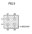
- the focal spots A of beams emitted to the samples are greater than the sizes S1, S2, S3 and S4 of the samples, as shown in FIG. 5.
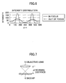
- FIG. 6 is a graph showing a comparison in the intensity distribution between the spots of beams in focus and out of focus emitted to a sample. As is also evident from this figure, off-focus spots A have an almost uniform distribution of intensity within the size-S1, -S2, -S3 and -S4 spots on the biochip.
- Each spot on the biochip is excited by this defocused beam of laser light and emits fluorescent light.
- This fluorescent light passes through the objective lens 5, the dichroic mirror 4 and a filter 7, and forms an image on the detector 9 by means of a lens 8.
- the position of the image-forming lens 8 is pre-adjusted so that both the image-formed surface of the detector 9 and the surface of the biochip 6 have the same focal length.
- spots on the biochip are excited in their entirety under an almost uniform distribution of light intensity. Consequently, it is possible to easily obtain a fluorescent image virtually free from effects due to the intensity distribution of excitation light.
- the biochip is mounted at a position on this side of the focal point of the objective lens 5.
- the biochip may be mounted at a position on the far side of the focal point, as shown in FIG. 7. This method of mounting is advantageous since a working distance d increases, thereby facilitating such work as mounting or removing the biochip.
- an image of spots on the biochip be formed on the detector 9 in an out of focus manner.
- This strategy makes it possible to reduce intensity bias in the detector (e.g., CCD) or a subsequent A/D converter, and thus widen the dynamic range of measurement.
- biochip 6 itself at an angle to the axis of incidence, rather than inclining the incident light, while keeping the optical axis of the incident light vertical.
- the present invention has the following advantageous effects:
- the biochip reader may be configured in such a manner that an emitted light beam is made obliquely incident on a sample. As a result, a fluorescent image and the image of excitation light from the sample are separated from each other, and so background noise due to the excitation light can be removed.
- the biochip reader may be configured such that a fluorescent image and the reflection image of excitation light from samples form at positions on the detector distant from each other. As a result, it is possible to easily remove the reflection image during the image processing stage.
Landscapes
- Health & Medical Sciences (AREA)
- Chemical & Material Sciences (AREA)
- Immunology (AREA)
- Physics & Mathematics (AREA)
- Life Sciences & Earth Sciences (AREA)
- Analytical Chemistry (AREA)
- Biochemistry (AREA)
- General Health & Medical Sciences (AREA)
- General Physics & Mathematics (AREA)
- Nuclear Medicine, Radiotherapy & Molecular Imaging (AREA)
- Pathology (AREA)
- Chemical Kinetics & Catalysis (AREA)
- Optics & Photonics (AREA)
- Investigating, Analyzing Materials By Fluorescence Or Luminescence (AREA)
Applications Claiming Priority (2)
| Application Number | Priority Date | Filing Date | Title |
|---|---|---|---|
| JP2001002264 | 2001-01-10 | ||
| JP2001002264A JP3824135B2 (ja) | 2001-01-10 | 2001-01-10 | バイオチップ読取り装置 |
Publications (3)
| Publication Number | Publication Date |
|---|---|
| EP1223421A2 true EP1223421A2 (fr) | 2002-07-17 |
| EP1223421A3 EP1223421A3 (fr) | 2002-07-24 |
| EP1223421B1 EP1223421B1 (fr) | 2007-11-28 |
Family
ID=18870802
Family Applications (1)
| Application Number | Title | Priority Date | Filing Date |
|---|---|---|---|
| EP01120597A Expired - Lifetime EP1223421B1 (fr) | 2001-01-10 | 2001-08-29 | Lecteur de biopuce |
Country Status (4)
| Country | Link |
|---|---|
| US (1) | US6494373B2 (fr) |
| EP (1) | EP1223421B1 (fr) |
| JP (1) | JP3824135B2 (fr) |
| DE (1) | DE60131626T2 (fr) |
Cited By (3)
| Publication number | Priority date | Publication date | Assignee | Title |
|---|---|---|---|---|
| EP1283416A3 (fr) * | 2001-08-09 | 2003-05-28 | Yokogawa Electric Corporation | Lecteur de biopuces et dispositif de formation d'images fluorométriques |
| WO2005040774A1 (fr) * | 2003-10-20 | 2005-05-06 | Infineon Technologies Ag | Mesure optique d'elements de dispositif par illumination sur reseau de petites lentilles |
| US8119995B2 (en) | 2005-07-21 | 2012-02-21 | Koninklijke Philips Electronics N.V. | Device for detection of excitation using a multiple spot arrangement |
Families Citing this family (20)
| Publication number | Priority date | Publication date | Assignee | Title |
|---|---|---|---|---|
| US6371370B2 (en) * | 1999-05-24 | 2002-04-16 | Agilent Technologies, Inc. | Apparatus and method for scanning a surface |
| US6789040B2 (en) | 2000-08-22 | 2004-09-07 | Affymetrix, Inc. | System, method, and computer software product for specifying a scanning area of a substrate |
| JP3741051B2 (ja) * | 2001-05-10 | 2006-02-01 | 横河電機株式会社 | バイオチップ読取装置 |
| US6913200B2 (en) * | 2002-11-20 | 2005-07-05 | Agilent Technologies, Inc. | Scanning parameterization for biopolymeric array scanner |
| JP2004191160A (ja) | 2002-12-11 | 2004-07-08 | Yokogawa Electric Corp | バイオチップの測定方法および測定装置 |
| DE10361569A1 (de) * | 2003-12-23 | 2005-07-21 | Robert Bosch Gmbh | Optisches Abbildungssystem |
| JP2006058044A (ja) * | 2004-08-18 | 2006-03-02 | Yokogawa Electric Corp | バイオチップ用カートリッジおよびバイオチップ読取装置 |
| JP4676539B2 (ja) * | 2009-02-25 | 2011-04-27 | 古河電気工業株式会社 | ラテラルフロー型蛍光イムノクロマト法用の標的物質を定量的に検出する装置及びその方法 |
| US8449842B2 (en) * | 2009-03-19 | 2013-05-28 | Thermo Scientific Portable Analytical Instruments Inc. | Molecular reader |
| EP2533033A4 (fr) * | 2010-02-03 | 2013-07-10 | Uchrezhdenie Rossiiskoi Akademii Nauk Inst Molekulyarnoi Biolog Im V A Engelgardta Ran Imb Ran | Dispositif pour l'analyse de micropuces biologiques luminescentes |
| CN103792190B (zh) * | 2012-10-31 | 2016-06-29 | 光宝科技股份有限公司 | 光学测量装置及光学测量方法 |
| KR101526495B1 (ko) * | 2013-04-29 | 2015-06-05 | 주식회사 인포피아 | 바이오 센서의 식별정보 판독 장치 |
| US9678323B2 (en) * | 2014-06-10 | 2017-06-13 | President And Fellows Of Harvard College | High throughput multichannel fluorescence microscopy with microlens arrays |
| WO2016156516A2 (fr) | 2015-03-31 | 2016-10-06 | Samantree Medical Sa | Systèmes et procédés d'imagerie en salle d'opération d'un tissu frais réséqué lors d'une chirurgie dans un but d'évaluation pathologique |
| CN104865262A (zh) * | 2015-06-15 | 2015-08-26 | 黄浩 | 一种便携式生物芯片检测装置 |
| JP6439810B2 (ja) | 2017-02-06 | 2018-12-19 | 横河電機株式会社 | バイオチップ、バイオチップユニット、バイオチップ読取装置、及びバイオチップ製造方法 |
| US11747603B2 (en) | 2017-10-31 | 2023-09-05 | Samantree Medical Sa | Imaging systems with micro optical element arrays and methods of specimen imaging |
| US10928621B2 (en) | 2017-10-31 | 2021-02-23 | Samantree Medical Sa | Sample dishes for use in microscopy and methods of their use |
| US10539776B2 (en) | 2017-10-31 | 2020-01-21 | Samantree Medical Sa | Imaging systems with micro optical element arrays and methods of specimen imaging |
| CN119125077A (zh) * | 2024-09-18 | 2024-12-13 | 清华大学深圳国际研究生院 | 一种用于ca125检测的适配体生物传感器及方法 |
Family Cites Families (15)
| Publication number | Priority date | Publication date | Assignee | Title |
|---|---|---|---|---|
| US5112134A (en) * | 1984-03-01 | 1992-05-12 | Molecular Devices Corporation | Single source multi-site photometric measurement system |
| CA1301324C (fr) * | 1986-05-20 | 1992-05-19 | Hideki Hosoya | Appareil d'enregistrement et de lecture optiques d'informations |
| US4892409A (en) * | 1988-07-14 | 1990-01-09 | Smith Harry F | Photometric apparatus for multiwell plates having a positionable lens assembly |
| US5122644A (en) * | 1988-11-17 | 1992-06-16 | Alps Electric Co., Ltd. | Optical code reading device with autofocussing |
| US5128528A (en) * | 1990-10-15 | 1992-07-07 | Dittler Brothers, Inc. | Matrix encoding devices and methods |
| WO1996023213A1 (fr) * | 1995-01-23 | 1996-08-01 | Murray Anthony J | Analyse de molecules biologiques |
| DE19653413C2 (de) * | 1996-12-22 | 2002-02-07 | Stefan Hell | Rastermikroskop, bei dem eine Probe in mehreren Probenpunkten gleichzeitig optisch angeregt wird |
| US5827748A (en) * | 1997-01-24 | 1998-10-27 | The United States Of America As Represented By The Secretary Of The Navy | Chemical sensor using two-dimensional lens array |
| DE19725050C2 (de) * | 1997-06-13 | 1999-06-24 | Fraunhofer Ges Forschung | Anordnung zur Detektion biochemischer oder chemischer Substanzen mittels Fluoreszenzlichtanregung und Verfahren zu deren Herstellung |
| DE19748211A1 (de) * | 1997-10-31 | 1999-05-06 | Zeiss Carl Fa | Optisches Array-System und Reader für Mikrotiterplatten |
| US6160618A (en) * | 1998-06-19 | 2000-12-12 | Board Of Regents, The University Of Texas System | Hyperspectral slide reader |
| AU4651200A (en) * | 1999-04-21 | 2000-11-02 | Chromagen | A novel scanning spectrophotometer for high throughput fluorescence detection |
| DE19919092A1 (de) * | 1999-04-27 | 2000-11-02 | Zeiss Carl Jena Gmbh | Anordnung zur optischen Auswertung eines Gegenstandsarrays |
| US6371370B2 (en) * | 1999-05-24 | 2002-04-16 | Agilent Technologies, Inc. | Apparatus and method for scanning a surface |
| WO2001001112A1 (fr) * | 1999-06-26 | 2001-01-04 | Packard Instrument Company, Inc. | Lecteur pour microplaques |
-
2001
- 2001-01-10 JP JP2001002264A patent/JP3824135B2/ja not_active Expired - Fee Related
- 2001-08-23 US US09/935,855 patent/US6494373B2/en not_active Expired - Fee Related
- 2001-08-29 EP EP01120597A patent/EP1223421B1/fr not_active Expired - Lifetime
- 2001-08-29 DE DE60131626T patent/DE60131626T2/de not_active Expired - Lifetime
Cited By (4)
| Publication number | Priority date | Publication date | Assignee | Title |
|---|---|---|---|---|
| EP1283416A3 (fr) * | 2001-08-09 | 2003-05-28 | Yokogawa Electric Corporation | Lecteur de biopuces et dispositif de formation d'images fluorométriques |
| WO2005040774A1 (fr) * | 2003-10-20 | 2005-05-06 | Infineon Technologies Ag | Mesure optique d'elements de dispositif par illumination sur reseau de petites lentilles |
| US7084966B2 (en) | 2003-10-20 | 2006-08-01 | Infineon Technologies Ag | Optical measurement of device features using lenslet array illumination |
| US8119995B2 (en) | 2005-07-21 | 2012-02-21 | Koninklijke Philips Electronics N.V. | Device for detection of excitation using a multiple spot arrangement |
Also Published As
| Publication number | Publication date |
|---|---|
| US6494373B2 (en) | 2002-12-17 |
| DE60131626T2 (de) | 2008-10-23 |
| JP3824135B2 (ja) | 2006-09-20 |
| DE60131626D1 (de) | 2008-01-10 |
| EP1223421B1 (fr) | 2007-11-28 |
| JP2002207007A (ja) | 2002-07-26 |
| EP1223421A3 (fr) | 2002-07-24 |
| US20020088858A1 (en) | 2002-07-11 |
Similar Documents
| Publication | Publication Date | Title |
|---|---|---|
| US6494373B2 (en) | Biochip reader | |
| US5585639A (en) | Optical scanning apparatus | |
| US6750963B2 (en) | Imaging systems for signals on a surface | |
| US6471916B1 (en) | Apparatus and method for calibration of a microarray scanning system | |
| EP1650551B1 (fr) | Lecteur de biopuce | |
| US20090032736A1 (en) | Biochip reader and fluorometric imaging apparatus | |
| US8023162B2 (en) | Hexagonal site line scanning method and system | |
| US6563584B1 (en) | Method and device for fluorescence measurement | |
| US20030160957A1 (en) | Scanning system and method for scanning a plurality of samples | |
| JP2001108684A (ja) | Dna検査方法及びdna検査装置 | |
| US6630680B2 (en) | Scanner having confocal optical system, method for producing focus position data of confocal optical system of scanner having confocal optical system and method for producing digital data of scanner having confocal optical system | |
| US6670198B2 (en) | Test piece and system for reading out image information from the test piece | |
| JP2002005834A (ja) | 蛍光標識物の分布計測装置 | |
| JP2001506015A (ja) | 複数の試料個所で同時に試料を光励起する走査顕微鏡 | |
| JP3858650B2 (ja) | Dna検査方法及びその装置 | |
| JP2003232733A (ja) | 蛍光画像検出方法及びその装置並びにdna検査方法及びその装置 | |
| JP2003057557A (ja) | バイオチップ読取装置 | |
| US7042565B2 (en) | Fluorescent microarray analyzer | |
| CN116507963B (zh) | 超分辨检测系统及超分辨检测方法 | |
| JP2001249077A (ja) | 複数の試料点から蛍光を検出するための装置 | |
| JP2004354344A (ja) | 光源装置及びその光源装置が適用される生体分子解析装置 | |
| JP3850181B2 (ja) | 光計測方法および装置 | |
| RU188251U1 (ru) | Устройство для сканирования биочипов | |
| EP1933131A1 (fr) | Système et procédé efficaces de détection de luminescence | |
| WO2016157458A1 (fr) | Appareil de mesure, système de mesure, procédé de traitement de chaîne de signal, et programme |
Legal Events
| Date | Code | Title | Description |
|---|---|---|---|
| PUAI | Public reference made under article 153(3) epc to a published international application that has entered the european phase |
Free format text: ORIGINAL CODE: 0009012 |
|
| PUAL | Search report despatched |
Free format text: ORIGINAL CODE: 0009013 |
|
| AK | Designated contracting states |
Kind code of ref document: A2 Designated state(s): AT BE CH CY DE DK ES FI FR GB GR IE IT LI LU MC NL PT SE TR |
|
| AX | Request for extension of the european patent |
Free format text: AL;LT;LV;MK;RO;SI |
|
| AK | Designated contracting states |
Kind code of ref document: A3 Designated state(s): AT BE CH CY DE DK ES FI FR GB GR IE IT LI LU MC NL PT SE TR |
|
| AX | Request for extension of the european patent |
Free format text: AL;LT;LV;MK;RO;SI |
|
| 17P | Request for examination filed |
Effective date: 20020829 |
|
| AKX | Designation fees paid |
Designated state(s): DE GB |
|
| 17Q | First examination report despatched |
Effective date: 20040628 |
|
| 17Q | First examination report despatched |
Effective date: 20040628 |
|
| GRAP | Despatch of communication of intention to grant a patent |
Free format text: ORIGINAL CODE: EPIDOSNIGR1 |
|
| GRAS | Grant fee paid |
Free format text: ORIGINAL CODE: EPIDOSNIGR3 |
|
| GRAA | (expected) grant |
Free format text: ORIGINAL CODE: 0009210 |
|
| AK | Designated contracting states |
Kind code of ref document: B1 Designated state(s): DE GB |
|
| REF | Corresponds to: |
Ref document number: 60131626 Country of ref document: DE Date of ref document: 20080110 Kind code of ref document: P |
|
| PLBE | No opposition filed within time limit |
Free format text: ORIGINAL CODE: 0009261 |
|
| STAA | Information on the status of an ep patent application or granted ep patent |
Free format text: STATUS: NO OPPOSITION FILED WITHIN TIME LIMIT |
|
| 26N | No opposition filed |
Effective date: 20080829 |
|
| PGFP | Annual fee paid to national office [announced via postgrant information from national office to epo] |
Ref country code: GB Payment date: 20120829 Year of fee payment: 12 |
|
| PGFP | Annual fee paid to national office [announced via postgrant information from national office to epo] |
Ref country code: DE Payment date: 20130821 Year of fee payment: 13 |
|
| GBPC | Gb: european patent ceased through non-payment of renewal fee |
Effective date: 20130829 |
|
| PG25 | Lapsed in a contracting state [announced via postgrant information from national office to epo] |
Ref country code: GB Free format text: LAPSE BECAUSE OF NON-PAYMENT OF DUE FEES Effective date: 20130829 |
|
| REG | Reference to a national code |
Ref country code: DE Ref legal event code: R119 Ref document number: 60131626 Country of ref document: DE |
|
| REG | Reference to a national code |
Ref country code: DE Ref legal event code: R119 Ref document number: 60131626 Country of ref document: DE Effective date: 20150303 |
|
| PG25 | Lapsed in a contracting state [announced via postgrant information from national office to epo] |
Ref country code: DE Free format text: LAPSE BECAUSE OF NON-PAYMENT OF DUE FEES Effective date: 20150303 |