EP1223437A2 - Couche antiréfléchissante pour lumière ultraviolette - Google Patents
Couche antiréfléchissante pour lumière ultraviolette Download PDFInfo
- Publication number
- EP1223437A2 EP1223437A2 EP01130830A EP01130830A EP1223437A2 EP 1223437 A2 EP1223437 A2 EP 1223437A2 EP 01130830 A EP01130830 A EP 01130830A EP 01130830 A EP01130830 A EP 01130830A EP 1223437 A2 EP1223437 A2 EP 1223437A2
- Authority
- EP
- European Patent Office
- Prior art keywords
- approx
- layer
- optical component
- component according
- layers
- Prior art date
- Legal status (The legal status is an assumption and is not a legal conclusion. Google has not performed a legal analysis and makes no representation as to the accuracy of the status listed.)
- Withdrawn
Links
Images



Classifications
-
- G—PHYSICS
- G02—OPTICS
- G02B—OPTICAL ELEMENTS, SYSTEMS OR APPARATUS
- G02B1/00—Optical elements characterised by the material of which they are made; Optical coatings for optical elements
- G02B1/10—Optical coatings produced by application to, or surface treatment of, optical elements
- G02B1/11—Anti-reflection coatings
- G02B1/113—Anti-reflection coatings using inorganic layer materials only
- G02B1/115—Multilayers
Definitions
- the invention relates to an optical component with little Reflectance for ultraviolet light from a wavelength range between approx. 180 nm and approx. 370 nm for a large one Incidence angle range, in particular up to at least about 40 °.
- the need for high-performing products is increasing optical components with low reflectance for ultraviolet light from a wavelength range between approx. 180 nm and approx. 370 nm.
- Light from this wavelength range is used for example in microlithography systems for manufacturing of highly integrated semiconductor components or other finely structured components with the help of wafer steppers or wafer scanners.
- multilayer systems are also used several superimposed layers of dielectric Materials with different refractive indices are used, which usually have layers of a high refractive index Material and layers of a relatively low refractive index Material are arranged alternately one above the other.
- the anti-reflective coating has a homogeneous effect on the entire coated surface and for all occurring optical angle of incidence typically shows in the range between vertical incidence and at least approx. 40 ° incidence angle lie.
- an optical component is not only in the range determined by the type of light source
- Working wavelength is transparent in the ultraviolet range, but also in a wavelength range of the visible Light, for example between approximately 500 nm and approximately 700 nm.
- a simultaneous reduction in reflection also for the visible Spectrum facilitates alignment between mask and substrate during exposure.
- a dual range anti-reflective coating for optical components of a processing laser is in the DE 198 31 392 shown. That for a working wavelength of 248 nm multi-layer system consists of nine individual layers, which in turn are made of magnesium fluoride as a low-index material and aluminum oxide as a high-index Material. The first closest to the substrate Layer in all embodiments consists of magnesium fluoride, and the layer thickness of the magnesium fluoride layer varies irregularly between approx. 25 nm and approx. 150 nm. These layers are said to have good laser resistance. For magnesium fluoride / aluminum oxide alternating layer systems with a very similar structure in terms of layer sequence and Layer thickness distribution was however after several years Use of crack formation combined with delamination observed whereby the life of such coatings and the optical components and systems equipped with it is limited.
- the invention has for its object a reflection reduction coating to suggest for optical components, those for ultraviolet light in the wavelength range between approx. 180 nm and approx. 370 nm and large angles of incidence effective anti-reflective coating up to at least approx. 40 ° enables and is characterized by high durability, in particular also under laser radiation.
- the invention proposes an optical one Component with the features of claim 1.
- advantageous Developments are specified in the dependent claims.
- the wording of all claims is by reference to Content of the description made.
- An anti-reflection multilayer system is characterized in that the adjacent to the substrate first layer essentially free of magnesium fluoride and that none of the layers has a layer thickness of more than approx. (0.5 ⁇ ), where ⁇ is the working wavelength from the ultraviolet wavelength range. So it should be first layer does not contain or does not contain magnesium fluoride of this material. In any case, one should existing amount of magnesium fluoride should be so small that the properties of this first layer are not determined by the Properties of magnesium fluoride significantly determined become. It is particularly favorable if none of the layers has a layer thickness of more than approx. (0.35 ⁇ ). As The layer thicknesses of the low refractive index have become particularly critical Proven material, which is preferred is a fluoride, in particular magnesium fluoride. Here the layer thickness should have a value of approx. 0.3 ⁇ none of the layers exceed.
- the invention and its advantageous developments show that it is for the creation of permanent laser-resistant anti-reflective coatings with the optical mentioned above Properties are required from the theoretically infinite large variety of optically suitable multilayer systems select the one with regard to the choice of materials for the layer closest to the substrate and with regard to maximum Layer thicknesses meet the specified boundary conditions.
- this was due to its low refractive index and the good processability conventionally in many cases
- Magnesium fluoride used identified as critical material unlike traditional proposals not used as the first layer next to the substrate should be.
- the layer thicknesses of this Material should be kept as small as possible. This is magnesium fluoride for the first time as a "mechanical weak link" such coatings have been identified.
- Whose negative influence on the durability of the anti-reflective coating can be achieved by using suitable thin individual layer thicknesses and minimize the total layer thickness as small as possible.
- multilayer systems build up that have no more than six individual layers.
- Laser stability of the coating alone be improved that the likelihood of Shift degradation leading to errors in the multiple shift is usually less the less layers are applied Need to become.
- Errors can especially be impurities, Defects or inclusions act that local absorption increase and thereby to an uneven radiation exposure can lead the shift.
- a reduction in the number of shifts also leads to process simplification, which costs for the provision of the coated optical components can decrease.
- the ratio between the sum of the layer thicknesses of the Layers of low refractive index material and the sum of the Layer thicknesses of the layers made of highly refractive material is below approximately 1.5, in particular below approximately 1.2. This may result in the build-up of thermal Tensions in the layer system and between the layer system and Favorably counteracted substrate and inner layer tensions.
- Fig. 1 is a schematic section through the surface area an optical component 1 shown that a Substrate 2 made of one for ultraviolet light with a wavelength of approx. 248 nm transparent material.
- a Substrate 2 made of one for ultraviolet light with a wavelength of approx. 248 nm transparent material.
- a multi-layer anti-reflective coating to reduce reflection 4 with six superimposed layers 5 to 10 applied.
- the substrate can also consist of a crystalline material, in particular a fluoride, such as calcium fluoride.
- the highly refractive layer 5 closest to the substrate has a layer thickness of approx. 64.2 nm or approx. 0.26 ⁇ and represents the thickest single layer of the multilayer system 4.
- This layer is very thin with a layer thickness of approx. 10 nm.
- the layers 7, 8, 9, 10 above are aluminum oxide (13.4 nm), magnesium fluoride (37.2 nm), aluminum oxide (30.5 nm) and magnesium fluoride (52.1 nm) in this order.
- S denotes the substrate, a vertical one Dash (
- the Letter M stands for magnesium fluoride.
- none of the layers 5 to 10 are one Layer thickness of more than about 65 nm (or 0.26 ⁇ ) has that the thickest single layer of magnesium fluoride (outer layer 10) is only approx. 52.1 nm (approx. 0.21 ⁇ ) thick and that is closest to the substrate Layer through a metal oxide, namely aluminum oxide is formed.
- the total thickness of the multilayer arrangement 4 is about 207 nm below the working wavelength and is only about 0.83 ⁇ .
- the overall very thin coating 4 is almost the same thickness on parts made of high refractive index Material and low refractive index material, the Ratio between the sum of the layer thicknesses of the layers made of low-index material and the sum of the layer thicknesses of layers 5, 7, 9 made of highly refractive material approx. 0.92 close to one that represents a uniform distribution Value of 1.
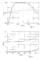
- an effective anti-reflective coating creates through which the degree of reflection broadband in the area from approx. 235 nm and approx. 292 nm to values below approx. 0.3 % is reduced at the working wavelength.
- Corresponding a bandwidth of approximately 1.24, the bandwidth being the Wavelength ratio between long-wave and short-wave Boundary of the area indicates where the reflectance is below of approx. 0.3%.
- This Dual area effect can align the reticle and Wafer (alignment) easier during the exposure, since here Alignment devices working with visible light (approx. 633 nm), that shine through the optical components, can be used without loss of transmission and / or false light or ghosting to inaccuracies comes.
- coatings according to the invention can also bring about a further reduction in reflection in the two wavelength ranges specified.
- a multi-layer system with ten individual layers is described as an example, which alternately consist of aluminum oxide and magnesium oxide.
- the layer system can be characterized with the above notation as follows: S
- the layer closest to the substrate again consists of aluminum oxide.
- the thickest magnesium oxide single layer has approx. 70.0 nm Layer thickness and lies approximately in the middle of the layer package.
- the ratio of the sum of the layer thicknesses from low refractive index Material and high refractive index material is approximately 0.9.
- FIGS. 4 to 6 A further example of a multiple coating according to the invention with six individual layers is explained with reference to FIGS. 4 to 6, which can be used particularly advantageously when an increase in transmission in the range of visible light is not necessary.
- This example is characterized with the above notation as follows: S
- This flat layer system has a total thickness of approx. 210 nm, which is less than the working wavelength.
- the the thickest single layer of magnesium fluoride lies approximately in the Middle of the layer package and has a layer thickness of 50.8 nm corresponding to approx. 0.2 ⁇ .
- the next layer to the substrate again consists of aluminum oxide.
- the relationship between the Sum of the layer thicknesses of low refractive index and high refractive index Material here is approximately 1.1, so there are reversed ones Ratios as in the layer according to FIGS. 1 and 2 before.
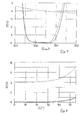
- FIGS. 4 to 6 The optical properties of the six-layer system are with reference to FIGS. 4 to 6, in each of which dash-dotted lines represent the values for an uncoated Show substrate while the solid line is calculated and the dotted line measured reflectance values or represent transmittance.
- the values apply the transmittance (Fig. 5) for a coated on both sides Substrate, in which both the light entry surface, how the light exit surface is coated. From Fig. 4 it follows that the reflectance is in the range of approx. 235 and approx. 290 nm broadband to values below approx. 0.2% residual reflection is reduced. This reduction in reflection takes place in the essentially without absorption or scattering effects, so that the Transmittance throughout in this wavelength range Values of approx. 99% or better reached. Leave accordingly itself with lenses coated in accordance with the invention or other transparent optical components (e.g. prisms, Plates or the like) bright optical systems build up.
- other transparent optical components e.g. prisms, Plates or the like
- 3 is similar to the embodiment according to FIG absolutely thickest layer the closest to the substrate aluminum oxide layer with 70.7 nm layer thickness.
- the thickest follows Magnesium fluoride single layer with a thickness of approx. 58.4 nm.
- the Ratio of the sum of the thicknesses of low refractive index and high refractive index material is approximately 0.93, the total thickness the multiple coating corresponds to 335 nm approx. 1.35 ⁇ .
- This layer system has very similar optical systems Properties like that according to FIGS. 4 to 6.
- the wavelength range effective reflection reduction lies here between approx. 235 and approx. 290 nm corresponding to a bandwidth of approximately 1.23.
- the residual reflection is in this area mostly below 0.2%.
- the anti-reflective coating has a large Angle of incidence up to at least 40 ° or even 50 ° reached optical components coated according to the invention, for example lenses, especially in high-aperture ones Optical systems are used where high optical Angle of incidence from this area can occur. moreover can also be lens surfaces with relatively strong deflection with a homogeneous effect over the entire lens surface entapt.
- the specified layer designs can be done by slight thickness corrections of the individual layers (to adapt to other substrate refractive indices) also on other substrate materials, such as calcium fluoride or barium fluoride, with essentially the same optical layer properties be effective.
- the layer designs which were previously explained on the basis of layers for a working wavelength of 248 nm, can also be used for other working wavelengths without significant changes with regard to wavelength-specific optical properties.
- the six-layer layer described first is selected, the optical properties of which are shown in FIG. 2 for a working wavelength of 248 nm. This curve of the degree of reflection over the wavelength corresponds to the dashed curve in FIG. 9.
- the layer design in (1) approximately results in the following layer design: S
- the absolute layer thicknesses of the individual layers can be achieved by inserting the appropriate working wavelength the absolute layer thicknesses of the individual layers for determine other working wavelengths. For example, let based on the layer design from (1) the geometric Layer thicknesses of the equivalent layer systems for 193 nm or 365 nm by multiplying the given (1) geometric Layer thicknesses with the factor 193/248 or 365/248 determine. In all cases the substrate material is more synthetic Quartz with the trade name Suprasil.
- the broadband area shifts more Reflection reduction in ultraviolet to longer wavelengths, where again at the working wavelength 365 nm Residual reflectance of less than 0.3% is achieved.
- This favorable value is in a broadband area, whose absolute width is larger than that of the thinner layers is, however, what is defined here as broadband Relationship between longer-wave and shorter-wave limits remains essentially constant. The reflection minimum in visible range shifts clearly to long wavelengths and is now around 950 nm.
- the examples show that with the coatings according to the invention optical component with low reflectance for Ultraviolet light from a wavelength range between approx. 180 nm and approx. 370 nm can be produced. It can be a great one Wavelength range of laser wavelengths widely used today be used in the field of microlithography. Special features of the coatings are optical Regards especially the very extensive and extraordinary broadband reflection reduction in the area of each Working wavelength. The layers are therefore also against process-related slight variations in layer thicknesses relative tolerant and can also be used for more curved surfaces sufficient effectiveness can be used. additionally this may result in an effective reflex reduction in the range of visible light. By avoiding too big Layer thicknesses of layers containing magnesium fluoride particularly durable coatings possible.
Landscapes
- Physics & Mathematics (AREA)
- Chemical & Material Sciences (AREA)
- Inorganic Chemistry (AREA)
- General Physics & Mathematics (AREA)
- Optics & Photonics (AREA)
- Surface Treatment Of Optical Elements (AREA)
- Laminated Bodies (AREA)
Applications Claiming Priority (2)
| Application Number | Priority Date | Filing Date | Title |
|---|---|---|---|
| DE10101017 | 2001-01-05 | ||
| DE10101017A DE10101017A1 (de) | 2001-01-05 | 2001-01-05 | Reflexionsminderungsbeschichtung für Ultraviolettlicht |
Publications (2)
| Publication Number | Publication Date |
|---|---|
| EP1223437A2 true EP1223437A2 (fr) | 2002-07-17 |
| EP1223437A3 EP1223437A3 (fr) | 2003-06-11 |
Family
ID=7670262
Family Applications (1)
| Application Number | Title | Priority Date | Filing Date |
|---|---|---|---|
| EP01130830A Withdrawn EP1223437A3 (fr) | 2001-01-05 | 2001-12-27 | Couche antiréfléchissante pour lumière ultraviolette |
Country Status (4)
| Country | Link |
|---|---|
| US (1) | US6825976B2 (fr) |
| EP (1) | EP1223437A3 (fr) |
| JP (1) | JP2002286909A (fr) |
| DE (1) | DE10101017A1 (fr) |
Cited By (2)
| Publication number | Priority date | Publication date | Assignee | Title |
|---|---|---|---|---|
| WO2008000841A3 (fr) * | 2006-06-28 | 2008-02-14 | Essilor Int | Article optique à revêtement anti-réflexion résistant à la température à rapport d'épaisseur optimisé de couches à faible indice et à fort indice |
| DE102011054837A1 (de) | 2011-10-26 | 2013-05-02 | Carl Zeiss Laser Optics Gmbh | Optisches Element |
Families Citing this family (16)
| Publication number | Priority date | Publication date | Assignee | Title |
|---|---|---|---|---|
| US20030090636A1 (en) * | 2001-10-26 | 2003-05-15 | Corning, Inc. | Anti-reflective coating on a photomask |
| JP4065530B2 (ja) * | 2002-05-22 | 2008-03-26 | キヤノン株式会社 | 反射防止膜、該反射防止膜を有する光学素子及び光学系 |
| CN101257980A (zh) * | 2002-09-19 | 2008-09-03 | 力特光电科技股份有限公司 | 表面活性纳米颗粒的防眩和抗反射涂层 |
| KR100643043B1 (ko) * | 2002-11-29 | 2006-11-10 | 마쯔시다덴기산교 가부시키가이샤 | 화상 표시 장치 및 그것에 이용하는 유리 기판의 평가 방법 |
| JP4433390B2 (ja) * | 2004-03-30 | 2010-03-17 | 株式会社ニコン | 反射防止膜並びにこの反射防止膜を有する光学素子及び光学系 |
| JP5201435B2 (ja) * | 2004-03-30 | 2013-06-05 | 株式会社ニコン | 光学系 |
| US7128984B2 (en) * | 2004-08-31 | 2006-10-31 | Corning Incorporated | Surfacing of metal fluoride excimer optics |
| EP2990839B1 (fr) * | 2004-09-16 | 2020-11-18 | Nikon Corporation | Système optique avec couche mince optique en mgf2 |
| DE102006014775A1 (de) * | 2006-03-30 | 2007-10-18 | Carl Zeiss Smt Ag | Verfahren und Behandlungsflüssigkeit zur Reinigung und Reparatur von optischen Elementen |
| US7894137B2 (en) * | 2007-04-24 | 2011-02-22 | The Board Of Regents For Oklahoma State University | Omnidirectional antireflection coating |
| DE102011054427A1 (de) | 2011-10-12 | 2013-04-18 | Carl Zeiss Laser Optics Gmbh | Verfahren zur Herstellung eines optischen Elements und optisches Element |
| DE112013002530T5 (de) * | 2012-05-15 | 2015-02-19 | Thermo Electron Scientific Instruments Llc | Ultrabreitbandige mehrschichtige dielektrische Strahlteilerbeschichtung |
| DE102015100091A1 (de) * | 2015-01-07 | 2016-07-07 | Rodenstock Gmbh | Schichtsystem und optisches Element mit einem Schichtsystem |
| CN109716180B (zh) * | 2016-09-15 | 2021-03-09 | 中央硝子株式会社 | 日照遮蔽构件 |
| WO2021021436A1 (fr) * | 2019-07-30 | 2021-02-04 | Corning Incorporated | Procédés de revêtement d'un substrat avec du fluorure de magnésium par dépôt de couche atomique |
| US11959164B2 (en) * | 2022-03-10 | 2024-04-16 | Yimin Hu | High damage threshold and highly reliable broad-band mid-IR coatings for high power fluoride fiber laser |
Family Cites Families (24)
| Publication number | Priority date | Publication date | Assignee | Title |
|---|---|---|---|---|
| JPS5040668B1 (fr) * | 1970-12-29 | 1975-12-25 | ||
| US4735488A (en) * | 1983-11-16 | 1988-04-05 | Optical Coating Laboratory, Inc. | Article and coating having improved reflectance suppression |
| LU86925A1 (fr) | 1987-06-19 | 1989-03-08 | Glaverbel | Article en verre transmettant la lumiere et presentant une faible reflexion speculaire |
| JP2620712B2 (ja) * | 1988-11-08 | 1997-06-18 | 株式会社 トプコン | 2波長反射防止多層膜 |
| AU7897591A (en) * | 1989-12-01 | 1991-06-26 | Viratec Thin Films, Inc. | Antireflection layer system with integral uv blocking properties |
| DD298849A5 (de) * | 1990-02-02 | 1992-03-12 | Jenoptik Carl Zeiss Jena Gmbh,De | Breitband-entspiegelungsschichtbelag |
| DD298850A5 (de) * | 1990-02-02 | 1992-03-12 | Jenoptik Carl Zeiss Jena Gmbh,De | Vielschicht-entspiegelungsbelag |
| US5233464A (en) * | 1991-03-20 | 1993-08-03 | Costich Verne R | Multilayer infrared filter |
| JP3232727B2 (ja) * | 1992-11-25 | 2001-11-26 | キヤノン株式会社 | 2波長反射防止膜 |
| US5532871A (en) * | 1992-11-25 | 1996-07-02 | Canon Kabushiki Kaisha | Two-wavelength antireflection film |
| US5604629A (en) * | 1993-07-27 | 1997-02-18 | The United States Of America As Represented By The Secretary Of The Navy | Discrete vacuum ultra violet reflective interference filter |
| US5728456A (en) * | 1996-02-01 | 1998-03-17 | Optical Coating Laboratory, Inc. | Methods and apparatus for providing an absorbing, broad band, low brightness, antireflection coating |
| JPH09258006A (ja) * | 1996-03-22 | 1997-10-03 | Canon Inc | 反射防止膜及びそれを施した光学系 |
| JP3924806B2 (ja) * | 1996-06-10 | 2007-06-06 | 株式会社ニコン | 反射防止膜 |
| JP4161387B2 (ja) | 1997-01-23 | 2008-10-08 | 株式会社ニコン | 多層反射防止膜 |
| JPH10253802A (ja) | 1997-03-07 | 1998-09-25 | Nikon Corp | 反射防止膜 |
| US5993898A (en) * | 1997-05-19 | 1999-11-30 | Nikon Corporation | Fabrication method and structure for multilayer optical anti-reflection coating, and optical component and optical system using multilayer optical anti-reflection coating |
| JP3624082B2 (ja) * | 1997-11-13 | 2005-02-23 | キヤノン株式会社 | 反射防止膜及びその製造方法 |
| US6066401A (en) | 1998-02-25 | 2000-05-23 | National Research Council Of Canada | Wide-band two-layer antireflection coating for optical surfaces |
| DE19831392A1 (de) * | 1998-07-14 | 2000-02-03 | Leica Microsystems | Zweibereichs-Reflexionsminderung für den sichtbaren Spektralbereich und einer Wellenlänge von: (248 +/- 15)NM |
| JP3943740B2 (ja) * | 1998-12-28 | 2007-07-11 | キヤノン株式会社 | 反射防止膜及びそれを施した光学系 |
| JP2001004803A (ja) * | 1999-06-17 | 2001-01-12 | Nikon Corp | 反射防止膜及び光学素子 |
| JP2001074904A (ja) * | 1999-09-02 | 2001-03-23 | Canon Inc | 二波長反射防止膜 |
| KR20010086056A (ko) * | 1999-09-30 | 2001-09-07 | 시마무라 기로 | 다층 박막을 갖는 광학소자 및 그것을 구비한 노광장치 |
-
2001
- 2001-01-05 DE DE10101017A patent/DE10101017A1/de not_active Withdrawn
- 2001-12-27 EP EP01130830A patent/EP1223437A3/fr not_active Withdrawn
- 2001-12-28 JP JP2001398906A patent/JP2002286909A/ja active Pending
-
2002
- 2002-01-07 US US10/036,536 patent/US6825976B2/en not_active Expired - Fee Related
Cited By (7)
| Publication number | Priority date | Publication date | Assignee | Title |
|---|---|---|---|---|
| WO2008000841A3 (fr) * | 2006-06-28 | 2008-02-14 | Essilor Int | Article optique à revêtement anti-réflexion résistant à la température à rapport d'épaisseur optimisé de couches à faible indice et à fort indice |
| US7692855B2 (en) | 2006-06-28 | 2010-04-06 | Essilor International Compagnie Generale D'optique | Optical article having a temperature-resistant anti-reflection coating with optimized thickness ratio of low index and high index layers |
| DE102011054837A1 (de) | 2011-10-26 | 2013-05-02 | Carl Zeiss Laser Optics Gmbh | Optisches Element |
| WO2013060853A1 (fr) | 2011-10-26 | 2013-05-02 | Carl Zeiss Laser Optics Gmbh | Élément optique |
| US9933711B2 (en) | 2011-10-26 | 2018-04-03 | Carl Zeiss Smt Gmbh | Optical element |
| US10642167B2 (en) | 2011-10-26 | 2020-05-05 | Carl Zeiss Smt Gmbh | Optical element |
| DE112012004501B4 (de) | 2011-10-26 | 2024-10-10 | Carl Zeiss Smt Gmbh | Optisches Element |
Also Published As
| Publication number | Publication date |
|---|---|
| DE10101017A1 (de) | 2002-07-11 |
| EP1223437A3 (fr) | 2003-06-11 |
| US6825976B2 (en) | 2004-11-30 |
| US20020105721A1 (en) | 2002-08-08 |
| JP2002286909A (ja) | 2002-10-03 |
Similar Documents
| Publication | Publication Date | Title |
|---|---|---|
| DE10101017A1 (de) | Reflexionsminderungsbeschichtung für Ultraviolettlicht | |
| DE69812450T3 (de) | Mehrschichtige Antireflexbeschichtungen für flach einfallendes Ultraviolettlicht | |
| EP1260835B1 (fr) | Filtre pour l'atténuation de rayons ultraviolets | |
| DE69223251T2 (de) | Elektrisch leitende, lichtdämpfende antireflektierende beschichtung | |
| DE102011075579A1 (de) | Spiegel und Projektionsbelichtungsanlage für die Mikrolithographie mit einem solchen Spiegel | |
| DE3218268C2 (fr) | ||
| DE2105280B2 (de) | Antireflexbelag | |
| DE102007054731A1 (de) | Optisches Element zur Reflexion von UV-Strahlung, Herstellungsverfahren dafür und Projektionsbelichtungsanlage damit | |
| WO2021115733A1 (fr) | Élément optique pourvu d'un revêtement protecteur, procédé pour le produire et agencement optique | |
| DE102015100091A1 (de) | Schichtsystem und optisches Element mit einem Schichtsystem | |
| DE102017105372B4 (de) | Transparentes Element mit einer Antireflex-Beschichtung und Verfahren zu dessen Herstellung | |
| EP1215512A2 (fr) | Revêtement anti-réfléchissant pour lumière ultraviolette à grands angles d'incidence | |
| DE112016000946T5 (de) | Antireflexfilm und optisches Bauelement | |
| DE102011054837A1 (de) | Optisches Element | |
| DE102010017106A1 (de) | Spiegel mit dielektrischer Beschichtung | |
| DE112016000959T5 (de) | Antireflexfilm und Verfahren zu dessen Herstellung und optisches Bauelement | |
| CH714953B1 (de) | Antireflex-Beschichtung mit stabiler Reflektivität und Farbe unter Winkel und unter Abrasion. | |
| EP1749222A1 (fr) | Miroir dielectrique a haute reflexion et son procede de production | |
| WO2010048975A1 (fr) | Revêtement d'oxyde d'hafnium | |
| DE102024205149A1 (de) | Reflektives optisches Element für streifenden Einfall | |
| WO2024240604A1 (fr) | Élément optique pour la plage de longueur d'onde ultraviolette | |
| WO2002086579A1 (fr) | Microscope de controle pour plusieurs gammes de longueurs d'onde et couche antireflet destinee a un microscope de controle pour plusieurs gammes de longueurs d'onde | |
| WO2004097467A1 (fr) | Element optique reflechissant, systeme optique et dispositif de lithographie euv | |
| DE2853004A1 (de) | Optisches system fuer ein kopiergeraet | |
| DE3025040A1 (de) | Lichtabsorbierender belag mit reflexionsverminderung |
Legal Events
| Date | Code | Title | Description |
|---|---|---|---|
| PUAI | Public reference made under article 153(3) epc to a published international application that has entered the european phase |
Free format text: ORIGINAL CODE: 0009012 |
|
| AK | Designated contracting states |
Kind code of ref document: A2 Designated state(s): AT BE CH CY DE DK ES FI FR GB GR IE IT LI LU MC NL PT SE TR |
|
| AX | Request for extension of the european patent |
Free format text: AL;LT;LV;MK;RO;SI |
|
| PUAL | Search report despatched |
Free format text: ORIGINAL CODE: 0009013 |
|
| AK | Designated contracting states |
Designated state(s): AT BE CH CY DE DK ES FI FR GB GR IE IT LI LU MC NL PT SE TR |
|
| AX | Request for extension of the european patent |
Extension state: AL LT LV MK RO SI |
|
| 17P | Request for examination filed |
Effective date: 20031209 |
|
| AKX | Designation fees paid |
Designated state(s): DE FR GB NL |
|
| RAP1 | Party data changed (applicant data changed or rights of an application transferred) |
Owner name: CARL ZEISS SMT AG |
|
| 17Q | First examination report despatched |
Effective date: 20040216 |
|
| STAA | Information on the status of an ep patent application or granted ep patent |
Free format text: STATUS: THE APPLICATION HAS BEEN WITHDRAWN |
|
| 18W | Application withdrawn |
Effective date: 20051216 |