EP1223670A2 - Oscillateur commandé en tension pour modulation de fréquence - Google Patents
Oscillateur commandé en tension pour modulation de fréquence Download PDFInfo
- Publication number
- EP1223670A2 EP1223670A2 EP01129646A EP01129646A EP1223670A2 EP 1223670 A2 EP1223670 A2 EP 1223670A2 EP 01129646 A EP01129646 A EP 01129646A EP 01129646 A EP01129646 A EP 01129646A EP 1223670 A2 EP1223670 A2 EP 1223670A2
- Authority
- EP
- European Patent Office
- Prior art keywords
- voltage
- oscillator
- connection
- frequency
- capacitance
- Prior art date
- Legal status (The legal status is an assumption and is not a legal conclusion. Google has not performed a legal analysis and makes no representation as to the accuracy of the status listed.)
- Granted
Links
Images
Classifications
-
- H—ELECTRICITY
- H03—ELECTRONIC CIRCUITRY
- H03C—MODULATION
- H03C3/00—Angle modulation
- H03C3/10—Angle modulation by means of variable impedance
- H03C3/12—Angle modulation by means of variable impedance by means of a variable reactive element
- H03C3/22—Angle modulation by means of variable impedance by means of a variable reactive element the element being a semiconductor diode, e.g. varicap diode
Definitions
- the present invention relates to a voltage controlled Oscillator (VCO, Voltage-Controlled Oscillator) for frequency modulation (FM, Frequency Modulation).
- VCO voltage controlled Oscillator
- FM Frequency Modulation
- Frequency modulation is one of the known modulation methods, which are used in digital modulation methods become.
- Such digital transmission systems are, for example DECT (Digital Enhanced Cordless Telecommunication), which is used with cordless phones or BLUETOOTH, which is the standard for an interface to designed for short-range wireless communication has been.
- the digitally encoded information on a carrier for example a high frequency sine wave, modulated.
- a carrier for example a high frequency sine wave
- the standards described lay down in their specifications Limits for the modulation stroke fixed.
- the modulation stroke is half the frequency difference between that Frequency at which a digital zero and that frequency with which a digital one is encoded if the to transmitting information is binary coded.
- the limits for the modulation stroke must not be exceeded or fallen short of become.
- VCOs can, for example be designed as an LC oscillator, in which the Vibration frequency at a certain tuning voltage Component tolerances, in particular inductance and capacitance, being affected.
- a voting range in to achieve normal operation for example Is 100 MHz
- the tuning range is the area of one Output signal of the VCO, which is between a minimally tunable Frequency and a maximum tunable frequency lies.
- a VCO with LC resonator has an inductance with a fixed inductance value of 2 nH.
- a voting area or tuning range of 2.2 - 2.8 GHz must be achieved the effective capacitance in the resonator can be adjusted from 1.62 - 2.62 pF his.
- BLUETOOTH requires a modulation capacity of 0.38 fF (Femtofarad) required.
- the same modulation capacity at the upper tuning limit of 2.8 GHz a modulation swing of 328 KHz, which is above the specified Limit is.
- the object of the present invention is a voltage-controlled Specify oscillator that without complex adjustment a required modulation stroke over a large tuning range comply.
- the coupling of the modulator component with the connection to Supply of the control voltage can be done in a simple manner be carried out that the dependence of the modulation stroke from the frequency set with the resonant circuit component of the VCO is compensated.
- the modulator component and the resonator component can work together be integrated in a resonator of the oscillator.
- the oscillator core can have a resonator, for example designed as an LC oscillator or as an RC oscillator can be.
- the frequency-determining resonance circuit component can, for example in the case of LC oscillators, the inductance or the capacitance of the resonator and, in the case of RC oscillators, the resistance or the capacitance of the oscillator.
- the capacitance can be used as a varactor be carried out, usually as a capacitance diode a junction capacitance which depends on the applied voltage depends.
- the resonant circuit component While with the resonant circuit component a very strong deviation the oscillator frequency depending on deviations an applied control voltage can be achieved only relatively small frequency deviations with the modulator component realized, which is usually by orders of magnitude are smaller than that of the resonance circuit component caused. Accordingly, the resonant circuit component is in one large range tunable while the modulator component is tunable in a very small area. For example can use the resonant circuit component to tune the frequency from 2.2 to 2.8 GHz can be achieved while that achievable with the frequency-determining modulator component Modulation stroke can be, for example, 160 KHz.
- Modulation stroke can be, for example, 160 KHz.
- the modulator component can be connected directly be connected to supply the control voltage.
- the modulator component comprises a first voltage controlled capacitance that too their control with the connection for supplying the control voltage connected is.
- the voltage controlled capacity can for example be a varactor, in particular a capacitance diode with a junction capacity, which is controllable is executed.
- the modulator component comprises a second voltage-controlled Capacity, which is parallel to the first voltage controlled Capacity switched and with one connection is coupled to supply a bias.
- Biasing for example, a capacitance diode in the reverse direction prevents the same from breaking through.
- an attenuation amplifier is provided, which with the Oscillator core is coupled and has the connection to which the output signal of the oscillator is provided.
- a voltage controlled oscillator usually an attenuation amplifier on, which is designed as an active circuit part and is a negative impedance to compensate for Provides losses in the resonator.
- an output signal can be derived, which has an oscillation or carrier frequency that is related to the control voltage is adjustable.
- the damping amplifier can include, for example, two cross-coupled transistors. The cross coupling can be capacitive, for example his.
- Such an oscillator is in a phase-locked loop, for example (PLL, phase locked loop) can be used.
- PLL phase locked loop
- the modulator component via at least one Coupling resistor with the connection for feeding the modulation signal connected.
- the coupling resistor can also use other components for DC voltage coupling or DC coupling can be used.
- the resonant circuit component comprises a third voltage-controlled Capacitance, which has at least one additional coupling resistor is connected to a reference potential connection and for their control with the connection for feeding the Control voltage is connected.
- the capacitance value of the third voltage controlled Capacity or the resonant circuit component is the capacitance value of the third voltage controlled Capacity or the resonant circuit component by a factor larger than the capacity value of the modulator component, which is 10 or more.
- the capacitance value of the modulator component can differ from this a parallel connection of several varactors.
- first coupling capacitances are provided Coupling of resonance circuit component with at least one inductance and second coupling capacitances for coupling the modulator component with the at least one inductor.
- the Coupling capacities can in addition to the coupling described at the same time a coupling of the oscillator core with the damping amplifier as well as with a supply potential connection realize.
- the capacity value of the second coupling capacities is the capacity value of the second coupling capacities by one Factor smaller than that of the first coupling capacities, which Is 10 or more.
- the resonant circuit device as well as its Coupling capacities have a capacity value that is large against the capacitance value of the modulator component and whose coupling capacities causes that with the control voltage a relatively large frequency deviation can be achieved, while with the modulation signal only a relative small frequency deviation, which the modulation stroke corresponds, can be achieved.
- the oscillator has a symmetrical circuit structure on.
- the symmetrical circuit structure enables especially high immunity to interference.
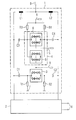
- the figure shows a voltage controlled oscillator with a Oscillator core 1 and an attenuation amplifier connected to it 2, the latter only drawn symbolically is.
- the oscillator core 1 has a symmetrical circuit structure on. At the attenuation amplifier 2 there is an output connection 8 provided on which a with a control voltage A frequency-tunable output signal is available. Farther a modulation signal B can be fed to the oscillator core, which the the oscillator over a transmission channel information to be transmitted, which is digitally coded, can deliver.
- the oscillator core 1 is designed as an LC oscillator.
- inductors L1, L2 are provided, each of which with a connection with a supply voltage connection 9 are connected. With their free connections are the inductors L1, L2 with coupling capacities C1, C2, C3, C4 as well connected to the attenuation amplifier 2.
- the resonant circuit component 3, which determines the resonant circuit frequency Control voltage A can be fed to an input is with one of the two coupling capacitances C1, C2 and each connected to a resistor R1, R2, the latter are connected to a reference potential connection 7.
- the Resonance circuit component 3 comprises several capacitance diodes, which cathode side with each other and with the connection to Supply of the control voltage A connected and which on the anode side with the coupling capacitances C1, C2 and the coupling resistors R1, R2 are connected.
- the modulator component 4 comprises two connected in parallel voltage-controlled capacitors 5, 6, each of which is from the cathode side interconnected capacitance diodes are formed are.
- the first voltage controlled capacitance 5 is on one input controlling the capacitance value the control voltage A feedable during the second voltage controlled Capacity 6 at an input controlling the capacity value a bias voltage C can be supplied.
- the first voltage controlled Capacitance 5 comprises capacitance diodes, which are on the cathode side with each other and with the connection for supplying the control voltage A and on the anode side, each with a coupling capacity C3, C4 are connected.
- control inputs from the first are voltage controlled Capacitance 5 and resonant circuit component 3 immediately connected with each other.
- the second voltage-controlled capacitance 6 comprises capacitance diodes, which on the cathode side with each other and with the connector are connected to supply the bias voltage C and on the anode side are connected to the coupling capacitors C3, C4. Accordingly, the first and second are voltage controlled capacitance connected in parallel.
- the one on the anode side in this parallel connection symmetrical circuit nodes formed on the capacitance diodes is in addition to the coupling capacitances C3, C4 with coupling resistors R3, R4 connected, which with their free end connected to the connection for supplying the modulation signal B. are.
- the capacitance values of the first coupling capacitances are C1, C2 large against the capacity values of the second coupling capacities C3, C4. Furthermore, varactor diodes, which are of a third voltage controlled capacitance in the resonant circuit component 3 are included, with their capacity values large against those capacitance values which result from the parallel connection the first and second voltage controlled capacities 5, 6 result.
- the capacitance values differ each at least by a factor of 10.
- the resonator is in the oscillator core 1 can be tuned in a frequency range of 2.2 - 2.8 GHz.
- the modulation stroke achievable with the modulation signal B is 160 kHz.
- the modulator component 4 is, however, according to the proposed In principle, the control voltage A for compensation purposes feedable, such that the modulation stroke of 160 kHz above the entire tunable frequency range of the oscillator stays the same. For example, if the control voltage A increases, for example from 1 to 2 volts, so decreases the capacitance of the resonant circuit component 3. Because about the resistors R1, R2 is the varactor 3 on the anode side and DC coupled with reference potential terminal 7. At the same time, the first voltage-controlled capacitance 5, in particular their capacitance diodes, more blocked. So is ensured that with the modulation signal B a relative minor change in capacitance in the modulator component 4 is effected. In the present embodiment is the controlling voltage of the modulation signal B free of a DC component and moves in one Range from 0 to 20 mV. The bias voltage C is +1 V. So it is ensured that the capacitance diodes in the reverse direction operate.
- the control voltage A can be measured and digitized and reprogrammed of the modulation signal B are used, so that over the entire tunable frequency range of the oscillator the modulation stroke is always constant.
- voltage controlled oscillators can be used for frequency modulation especially then also a constant modulation deviation over a wide frequency range have when the frequency-determining component of the Oscillators are tolerant.
- the modulation capacity that is the capacity of the modulator component 4 is therefore variable and depends on each valid control voltage A. This is achieved that part of the capacitance in the modulator device 4 is not placed on a fixed potential, but that the voltage-controlled capacitance 5 biased with the control voltage A. becomes.
Landscapes
- Inductance-Capacitance Distribution Constants And Capacitance-Resistance Oscillators (AREA)
- Digital Transmission Methods That Use Modulated Carrier Waves (AREA)
- Transmitters (AREA)
Applications Claiming Priority (2)
| Application Number | Priority Date | Filing Date | Title |
|---|---|---|---|
| DE10100113A DE10100113A1 (de) | 2001-01-03 | 2001-01-03 | Spannungsgesteuerter Oszillator zur Frequenzmodulation |
| DE10100113 | 2001-01-03 |
Publications (4)
| Publication Number | Publication Date |
|---|---|
| EP1223670A2 true EP1223670A2 (fr) | 2002-07-17 |
| EP1223670A3 EP1223670A3 (fr) | 2004-06-30 |
| EP1223670B1 EP1223670B1 (fr) | 2011-09-28 |
| EP1223670B8 EP1223670B8 (fr) | 2012-03-14 |
Family
ID=7669720
Family Applications (1)
| Application Number | Title | Priority Date | Filing Date |
|---|---|---|---|
| EP01129646A Expired - Lifetime EP1223670B8 (fr) | 2001-01-03 | 2001-12-12 | Oscillateur commandé en tension pour modulation de fréquence |
Country Status (3)
| Country | Link |
|---|---|
| US (1) | US6621364B2 (fr) |
| EP (1) | EP1223670B8 (fr) |
| DE (1) | DE10100113A1 (fr) |
Cited By (2)
| Publication number | Priority date | Publication date | Assignee | Title |
|---|---|---|---|---|
| US6700447B1 (en) | 2002-09-06 | 2004-03-02 | Telefonaktiebolaget Lm Ericsson (Publ) | Trimming of a two point phase modulator |
| WO2004034564A3 (fr) * | 2002-09-06 | 2004-11-11 | Ericsson Telefon Ab L M | Ajustage d'un modulateur de phase a deux points |
Families Citing this family (14)
| Publication number | Priority date | Publication date | Assignee | Title |
|---|---|---|---|---|
| EP1383238A1 (fr) * | 2002-07-16 | 2004-01-21 | Lucent Technologies Inc. | Dispositif à résistance négative accordable |
| US6917248B2 (en) * | 2002-07-18 | 2005-07-12 | Sige Semiconductor Inc. | Broadband voltage controlled oscillator supporting improved phase noise |
| JP3956795B2 (ja) * | 2002-08-09 | 2007-08-08 | 松下電器産業株式会社 | 変調機能付き電圧制御発振器 |
| CN1972117B (zh) * | 2002-10-03 | 2010-08-25 | 松下电器产业株式会社 | 电压控制振荡器和无线电通信设备 |
| GB2408400B (en) * | 2003-11-24 | 2006-05-03 | Zarlink Semiconductor Ltd | A circuit arrangement |
| GB2408401B (en) * | 2003-11-24 | 2006-05-03 | Zarlink Semiconductor Ltd | A network |
| DE102005006543B4 (de) * | 2004-02-12 | 2014-03-27 | Zarlink Semiconductor Ab | Direkt modulierter spannungsgesteuerter Oszillator auf CMOS-Basis |
| GB2411061B (en) * | 2004-02-12 | 2008-11-05 | Zarlink Semiconductor Ab | Directly modulated CMOS VCO |
| US7190237B2 (en) * | 2004-05-27 | 2007-03-13 | Continental Automotive, Inc. | Open-loop start-up method for a resonating device |
| DE102005003904A1 (de) * | 2005-01-27 | 2006-10-12 | Infineon Technologies Ag | Oszillatorschaltung |
| FR2905808B1 (fr) * | 2006-09-12 | 2008-12-26 | United Monolithic Semiconduct | Oscillateur hyperfrequence en technologie des circuits integres |
| US8222962B2 (en) * | 2007-09-28 | 2012-07-17 | Realtek Semiconductor Corp. | High-resolution digitally controlled oscillator and method thereof |
| US9810744B2 (en) * | 2014-01-02 | 2017-11-07 | Texas Instruments Incorporated | Resonant inductive sensing with reduced noise folding |
| CN113098503B (zh) * | 2021-04-08 | 2024-03-29 | 中国科学技术大学 | 一种基于mems谐振器的低功耗高分辨率宽带可调振荡器 |
Family Cites Families (10)
| Publication number | Priority date | Publication date | Assignee | Title |
|---|---|---|---|---|
| US4074209A (en) * | 1976-12-13 | 1978-02-14 | Rca Corporation | Wide range frequency modulation of narrow loop bandwidth phase-locked oscillators |
| JPS58107703A (ja) * | 1981-12-21 | 1983-06-27 | Matsushita Electric Ind Co Ltd | 電圧制御発振器 |
| US4503402A (en) * | 1982-08-19 | 1985-03-05 | General Electric Company | Voltage controlled oscillator having approximately constant modulation sensitivity |
| DE3447118A1 (de) * | 1984-12-22 | 1986-07-10 | Licentia Patent-Verwaltungs-Gmbh, 6000 Frankfurt | Pll-frequenzmodulator |
| DE3827429A1 (de) * | 1988-03-01 | 1989-09-14 | Licentia Gmbh | Spannungsgesteuerter oszillator mit leitungsresonator |
| US4904964A (en) * | 1988-12-27 | 1990-02-27 | Motorola, Inc. | Voltage control oscillator with modulation compensation |
| DE4241241A1 (de) * | 1992-12-08 | 1994-06-09 | Bosch Gmbh Robert | Frequenzmodulierter spannungsgesteuerter Oszillator |
| GB2338128B (en) * | 1998-06-03 | 2001-10-17 | Motorola Ltd | Circuit arrangement |
| US6218909B1 (en) * | 1998-10-23 | 2001-04-17 | Texas Insturments Israel Ltd. | Multiple frequency band voltage controlled oscillator |
| US6466099B2 (en) * | 2001-01-03 | 2002-10-15 | Motorola, Inc. | Voltage controlled oscillator (VCO) in colpitts configuration |
-
2001
- 2001-01-03 DE DE10100113A patent/DE10100113A1/de not_active Withdrawn
- 2001-12-12 EP EP01129646A patent/EP1223670B8/fr not_active Expired - Lifetime
-
2002
- 2002-01-03 US US10/040,213 patent/US6621364B2/en not_active Expired - Lifetime
Cited By (3)
| Publication number | Priority date | Publication date | Assignee | Title |
|---|---|---|---|---|
| US6700447B1 (en) | 2002-09-06 | 2004-03-02 | Telefonaktiebolaget Lm Ericsson (Publ) | Trimming of a two point phase modulator |
| WO2004034564A3 (fr) * | 2002-09-06 | 2004-11-11 | Ericsson Telefon Ab L M | Ajustage d'un modulateur de phase a deux points |
| US7053727B2 (en) | 2002-09-06 | 2006-05-30 | Telefonaktiebolaget Lm Ericsson (Publ) | Trimming of a two point phase modulator |
Also Published As
| Publication number | Publication date |
|---|---|
| US6621364B2 (en) | 2003-09-16 |
| EP1223670B1 (fr) | 2011-09-28 |
| US20020089387A1 (en) | 2002-07-11 |
| EP1223670A3 (fr) | 2004-06-30 |
| DE10100113A1 (de) | 2002-07-18 |
| EP1223670B8 (fr) | 2012-03-14 |
Similar Documents
| Publication | Publication Date | Title |
|---|---|---|
| EP1223670B1 (fr) | Oscillateur commandé en tension pour modulation de fréquence | |
| DE60005841T2 (de) | Variabler oszillator und filterschaltung | |
| DE19647383C2 (de) | Spannungsgesteuerte, veränderliche Abstimmschaltung | |
| DE102006011285B4 (de) | Schwingkreisanordnung mit digitaler Steuerung, Verfahren zur Erzeugung eines Schwingungssignals und digitaler Phasenregelkreis mit der Schwingkreisanordnung | |
| DE102007023795A1 (de) | Oszillator zum Erzeugen von unterschiedlichen Schwingungen | |
| DE102007022999A1 (de) | Oszillator | |
| DE69407902T2 (de) | Verstärkungsstufe und Oszillator | |
| DE102005048409A1 (de) | Verstärkeranordnung für Ultra-Breitband-Anwendungen und Verfahren | |
| DE3121642A1 (de) | "phasenstarre schleifenschaltung mit mehrfachrueckkopplung" | |
| DE69823415T2 (de) | Schaltungsanordnung zum Vermeiden von parasitären Oszillatorbetriebszuständen in einer Oszillatorschaltung | |
| EP1391030B1 (fr) | Circuit oscillateur commande en tension | |
| DE102007027612B4 (de) | Monolithisch integrierte Induktivität | |
| DE19808377A1 (de) | Vollintegrierbare spannungsgesteuerte Oszillatorschaltung | |
| EP1586183B1 (fr) | Ensemble oscillateur utilise a des fins de modulation de frequence | |
| EP0330983A2 (fr) | Oscillateur commandé en tension à résonateur à ligne | |
| DE69228671T2 (de) | Spannungsgesteuertes Teil | |
| DE3788196T2 (de) | Oszillator mit grossem Bereich. | |
| DE102004059987B4 (de) | Spannungsgesteuerte Oszillatorschaltung mit analoger und digitaler Ansteuerung und phasenverriegelte Regelschleife mit einer solchen Oszillatorschaltung | |
| DE69324446T2 (de) | Abstimmbarer Resonanzkreis für spannungsgesteuerten Oszillator | |
| EP0552642A1 (fr) | Radioémetteur et -récepteur avec circuit à bande de verrouillage de phase | |
| EP1386400B1 (fr) | Boucle a phase asservie | |
| EP1207619A2 (fr) | Circuit d'oscillateur | |
| EP0909018B1 (fr) | Oscillateur | |
| DE1252761B (fr) | ||
| DE60035688T2 (de) | Spannungsgesteuerter oszillator |
Legal Events
| Date | Code | Title | Description |
|---|---|---|---|
| PUAI | Public reference made under article 153(3) epc to a published international application that has entered the european phase |
Free format text: ORIGINAL CODE: 0009012 |
|
| AK | Designated contracting states |
Kind code of ref document: A2 Designated state(s): AT BE CH CY DE DK ES FI FR GB GR IE IT LI LU MC NL PT SE TR |
|
| AX | Request for extension of the european patent |
Free format text: AL;LT;LV;MK;RO;SI |
|
| PUAL | Search report despatched |
Free format text: ORIGINAL CODE: 0009013 |
|
| AK | Designated contracting states |
Kind code of ref document: A3 Designated state(s): AT BE CH CY DE DK ES FI FR GB GR IE IT LI LU MC NL PT SE TR |
|
| AX | Request for extension of the european patent |
Extension state: AL LT LV MK RO SI |
|
| 17P | Request for examination filed |
Effective date: 20041213 |
|
| AKX | Designation fees paid |
Designated state(s): DE FR GB |
|
| RIN1 | Information on inventor provided before grant (corrected) |
Inventor name: GETTA, KLAUS Inventor name: RASSOULI, FARAMARZ Inventor name: GREWING, CHRISTIAN Inventor name: MATTER, UDO |
|
| RAP1 | Party data changed (applicant data changed or rights of an application transferred) |
Owner name: INFINEON TECHNOLOGIES AG |
|
| 17Q | First examination report despatched |
Effective date: 20090810 |
|
| GRAP | Despatch of communication of intention to grant a patent |
Free format text: ORIGINAL CODE: EPIDOSNIGR1 |
|
| GRAS | Grant fee paid |
Free format text: ORIGINAL CODE: EPIDOSNIGR3 |
|
| GRAA | (expected) grant |
Free format text: ORIGINAL CODE: 0009210 |
|
| AK | Designated contracting states |
Kind code of ref document: B1 Designated state(s): DE FR GB |
|
| REG | Reference to a national code |
Ref country code: GB Ref legal event code: FG4D Free format text: NOT ENGLISH |
|
| REG | Reference to a national code |
Ref country code: DE Ref legal event code: R096 Ref document number: 50115962 Country of ref document: DE Effective date: 20111117 |
|
| RAP2 | Party data changed (patent owner data changed or rights of a patent transferred) |
Owner name: WI-LAN INC. |
|
| PLBE | No opposition filed within time limit |
Free format text: ORIGINAL CODE: 0009261 |
|
| STAA | Information on the status of an ep patent application or granted ep patent |
Free format text: STATUS: NO OPPOSITION FILED WITHIN TIME LIMIT |
|
| 26N | No opposition filed |
Effective date: 20120629 |
|
| REG | Reference to a national code |
Ref country code: DE Ref legal event code: R097 Ref document number: 50115962 Country of ref document: DE Effective date: 20120629 |
|
| PGFP | Annual fee paid to national office [announced via postgrant information from national office to epo] |
Ref country code: GB Payment date: 20141210 Year of fee payment: 14 Ref country code: DE Payment date: 20141209 Year of fee payment: 14 |
|
| PGFP | Annual fee paid to national office [announced via postgrant information from national office to epo] |
Ref country code: FR Payment date: 20141208 Year of fee payment: 14 |
|
| REG | Reference to a national code |
Ref country code: DE Ref legal event code: R119 Ref document number: 50115962 Country of ref document: DE |
|
| GBPC | Gb: european patent ceased through non-payment of renewal fee |
Effective date: 20151212 |
|
| REG | Reference to a national code |
Ref country code: FR Ref legal event code: ST Effective date: 20160831 |
|
| PG25 | Lapsed in a contracting state [announced via postgrant information from national office to epo] |
Ref country code: GB Free format text: LAPSE BECAUSE OF NON-PAYMENT OF DUE FEES Effective date: 20151212 Ref country code: DE Free format text: LAPSE BECAUSE OF NON-PAYMENT OF DUE FEES Effective date: 20160701 |
|
| PG25 | Lapsed in a contracting state [announced via postgrant information from national office to epo] |
Ref country code: FR Free format text: LAPSE BECAUSE OF NON-PAYMENT OF DUE FEES Effective date: 20151231 |