EP1224448B1 - Verfahren und apparat zur messung der geometrischen struktur eines optischen bauteils durch lichtübertragung - Google Patents
Verfahren und apparat zur messung der geometrischen struktur eines optischen bauteils durch lichtübertragung Download PDFInfo
- Publication number
- EP1224448B1 EP1224448B1 EP01965331A EP01965331A EP1224448B1 EP 1224448 B1 EP1224448 B1 EP 1224448B1 EP 01965331 A EP01965331 A EP 01965331A EP 01965331 A EP01965331 A EP 01965331A EP 1224448 B1 EP1224448 B1 EP 1224448B1
- Authority
- EP
- European Patent Office
- Prior art keywords
- component
- optical component
- wavefront
- illuminating
- measuring
- Prior art date
- Legal status (The legal status is an assumption and is not a legal conclusion. Google has not performed a legal analysis and makes no representation as to the accuracy of the status listed.)
- Expired - Lifetime
Links
Images








Classifications
-
- G—PHYSICS
- G01—MEASURING; TESTING
- G01M—TESTING STATIC OR DYNAMIC BALANCE OF MACHINES OR STRUCTURES; TESTING OF STRUCTURES OR APPARATUS, NOT OTHERWISE PROVIDED FOR
- G01M11/00—Testing of optical apparatus; Testing structures by optical methods not otherwise provided for
- G01M11/02—Testing optical properties
- G01M11/0242—Testing optical properties by measuring geometrical properties or aberrations
- G01M11/0257—Testing optical properties by measuring geometrical properties or aberrations by analyzing the image formed by the object to be tested
-
- G—PHYSICS
- G01—MEASURING; TESTING
- G01B—MEASURING LENGTH, THICKNESS OR SIMILAR LINEAR DIMENSIONS; MEASURING ANGLES; MEASURING AREAS; MEASURING IRREGULARITIES OF SURFACES OR CONTOURS
- G01B11/00—Measuring arrangements characterised by the use of optical techniques
- G01B11/24—Measuring arrangements characterised by the use of optical techniques for measuring contours or curvatures
- G01B11/255—Measuring arrangements characterised by the use of optical techniques for measuring contours or curvatures for measuring radius of curvature
Definitions
- the present invention relates to a method and an apparatus for measuring the geometric or optical structure of an optical component.
- the method according to the invention makes it possible to measure absolutely one or more polished surfaces or the index distribution of an optical component.
- Absolute measurement is a measure that does not require any prior knowledge of the component.
- the measurement of polished surfaces and / or index distributions is susceptible of many industrial applications. It is particularly useful in the ophthalmic field for the control or measurement of ophthalmic lenses; in this case, the production of complex surfaces requires the simultaneous determination of hundreds of coefficients.
- FR-A-2,710,162 or EP-A-0 644 411 in the name of the applicant describe a deflectometry apparatus in reflection or in transmission.
- This apparatus allows measurement by reflection or transmission of the geometric structure of an optical component.
- the principle of such a measuring device is to illuminate the optical component to be measured by a known wave surface radiation - in the simplest case a plane wave - and to measure the wavefront after reflection or transmission. on the optical component to be measured.
- the measurement of the wave surface after reflection or transmission makes it possible to go back to the geometrical characteristics of the component to be measured.
- WO-A-9705467 describes a similar device. This document proposes to calibrate the apparatus by measuring the transverse aberration of a reference ray after reflection or transmission by the component to be measured.
- the devices described in these documents actually work for only one surface of an optical component.
- the devices make it possible to determine the geometrical structure of the surface on which the known wave-surface light is reflected.
- the apparatuses make it possible to determine the geometrical structure of one of the surfaces of the optical component, if the other surface and the index of the component are known.
- transmission it is possible to determine the index distribution of the component, if the two surfaces of the component are known.
- US-A-5,825,476 proposes an apparatus for mapping an optical component. This document proposes to illuminate an optical component with a light having a known wavefront, then to collect on a network of microlenses the light transmitted through the component or reflected by it. The micro-lenses project transmitted or reflected light onto a frosted screen; the image of the frosted screen is recorded by a camera and is analyzed to determine the structure of the optical component, in comparison with a reference image. The result obtained in transmission is a power card of the component and in reflection, an altitude map of the component.
- this document proposes to proceed to two measurements, in two positions of the frosted screen, but without modifications in the system other than the position of the frosted screen. These two measurements make it possible, for each micro-lens, to determine the radius after transmission, by knowing two points for two positions of the frosted screen. The entry point is known before the measurement because it corresponds to a micro-lens of the input matrix. Knowing one of the surface of the component, it is then possible to determine the second surface of the component.
- This document like the three preceding documents, therefore only makes it possible to determine the geometry of a surface of the component.
- the geometry of the other surface of the component is assumed to be known for calculations.
- the wave fronts on the side of the same surface of the component are different.
- Hartmann or Shack-Hartmann deflectometry, or fringe deflectometry, or interferometric measurement can advantageously be used for the measurement step.
- the lighting steps include illuminating the component on one of its surfaces, and illuminating the component on the other of its surfaces.
- the first and second lights may have identical wave fronts.
- the illumination steps comprise illuminating the optical component with the same incident light, the method then comprising a step of reversing the optical component.
- the lighting steps include illuminating the component on only one of its surfaces.
- the first and second lights may have distinct wavefronts.
- the calculation step is performed by optimizing a merit function calculated from at least two measurement steps. It is also possible to provide a step of measuring the thickness of the component in at least one point.
- the measuring means comprise a microlens array. They can also include a network.
- the illumination means of the optical component by a first incident light, and the illumination means of the optical component by a second incident light respectively illuminate the component on each of its surfaces.
- the first and second lights may have identical wave fronts.
- the illumination means of the optical component by a first incident light and the illumination means of the optical component by a second incident light illuminate the same surface of the component.
- the first and second lights may have distinct wavefronts.
- the apparatus may further comprise means for measuring the thickness of the component.
- the invention rests as in the apparatuses of the applicant described in FR-A-2,710,162 or WO-A-9705467 , on the analysis of wave fronts - or rays perpendicular to them - after and before transmission by the component to be measured. It is possible to measure the wavefront of the light after transmission by the component to use, as in these documents, a deflectometry method with fringes, or a method of so-called Hartmann or Shack-Hartmann deflectometry. It is also possible to measure the wavefront of the light transmitted by interferometric methods, and for example by Mach-Zender interferometry, or by interferometry according to the method called lateral shearing interferometry.
- the invention proposes to carry out two measurements in transmission in two distinct optical configurations, and to deduce without preliminary assumptions the two surfaces of the component and their relative position.
- One possible solution consists of minimizing or maximizing a merit function by taking as variables the set of coefficients representative of the geometry of the glass so that, when the merit function is minimal - or maximum - the values taken by the variables correspond to to the values of each of the coefficients that define the geometric characteristics of the component.
- the optical configurations are distinct insofar as the crossing of the component is carried out by different optical paths.
- the wave surfaces are determined by Hartmann or Hartmann's deflectometry; the principle of this deflectometry is described in US-A-5,825,476 .
- the optical component to be measured is illuminated by a light having a known wavefront.
- the light transmitted by the optical component is applied to an array of micro-lenses, which form images in a plane represented by a frosted screen or by a matrix of charge-coupled sensors (CCD).
- CCD charge-coupled sensors
- the insertion of an optical component into the system induces a variation of the incident wavefront on the microlenses, and thus a variation of the position of the image point of each microlens; the analysis of the displacement of the image point of each micro-lens makes it possible to measure the variation of the wavefront caused by the insertion of the optical component into the system.
- Figure 1 shows a schematic representation of a first embodiment of an apparatus for carrying out the invention
- two different incident lights are used for the two transmission measurements according to two distinct configurations, and more specifically a light having a plane wavefront and a light having a spherical wavefront.
- the apparatus of FIG. 1 thus has a support (not shown) for receiving an optical component 2, which has a rear surface 4 and a front surface 6; the terms "forward” and “backward” are only used here to identify the surfaces, and do not necessarily correspond to the subsequent use of the component; in other words, the component can be arranged “upside down” in the apparatus.
- the apparatus further has a light source having a plane wavefront.
- a point source 8 and a lens 10 which generate a light incident on the rear surface 4 of the component to be measured with a plane wavefront.
- the apparatus also has a light source having a spherical wavefront.
- a second point source 12 which generates incident light on the back surface of the component with a spherical wavefront, may be used.
- a semi-reflecting plate 14 is used to illuminate the rear surface 4 of the component with the lights coming from the sources 8 and 12: the light coming from the source 8 and from the lens 10 passes through the semi-reflecting plate 14, whereas the light from the source 12 is reflected by the blade 14.
- the apparatus may further have means for measuring at one point the thickness of the component. It is possible to provide for example a measurement in reflection of the component on the axis of the device, on both sides of the component. Such a measurement makes it possible to determine the normal of the surfaces of the component at the intersection with the axis of the apparatus, as well as the thickness of the component on this axis. For these measurements, it is possible to use on the side of the rear surface as on the side of the surface before the means described in FR-A-2,710,162 or WO-A-9705467 , which are not described again here.
- Such a measurement of the thickness is not essential to the implementation of the invention; the thickness measurement makes it possible to accelerate the determination of the characteristics of the component. It remains possible not to measure the thickness of the component, and determine it during the optimization search described below.
- the apparatus then has means for determining the wavefront of the light transmitted by the component.
- means for determining the wavefront of the light transmitted by the component In the embodiment of the figure, as indicated above, one can use a Hartmann deflectometry, or a Shack-Hartmann deflectometry when microlenses are used; the apparatus thus has a microlens array 16, and an analysis plane 18, on which the microlenses form an image.
- This plan analysis can be made either by a frosted or directly by a CCD.
- the analysis of the image formed on the analysis plane makes it possible to determine the wavefront of the light transmitted through the component.
- Typical dimensions of the apparatus of FIG. 1 are as follows: the lens 10 is located on the main axis passing through the component 2 to be measured and the matrix 16 of microlenses; it has a diameter of 100 mm and a focal length of between 110 and 250 mm.
- the separating blade 14 has a diameter of 150 mm.
- the distance between the second source 12 (located on an axis perpendicular to the main axis) and the intersection point between the 14 and the main axis is of the order of 70 mm.
- the distance between this same point and the surface of the optical component 2 is also of the order of 70 mm.
- the distance between the component 2 and the Shack-Hartmann can also be between 0 and 30 mm.
- Sources 8 and 12 may be laser diodes or LEDs.
- the apparatus of FIG. 1 thus allows a wavefront measurement of two lights transmitted by the component.
- the apparatus makes it possible to measure in two distinct configurations the transmission of a known wavefront incident light through the component to be measured.
- the apparatus may optionally also allow a measurement of the thickness of the component at a point.
- the component is centered on the optical axis of the apparatus; as explained below, it is not necessary in the method of the invention that the component is precisely centered on the optical axis of the apparatus, and coarse positioning is sufficient.
- FIG. 2 shows a schematic representation of a second embodiment of an apparatus for implementing the invention.
- the apparatus therefore has a light source 20 generating a known wavefront light - in the example of the figure a spherical wavefront light.
- the light arrives on a component 22 mounted on a not shown support; the component has a rear surface 24 and a front surface 26.
- the apparatus then has means for determining the wavefront of the light transmitted by the component; as in the embodiment of FIG. 1, a microlens array 28 and an analysis plane 30 are used.
- the apparatus of FIG. 2 allows measurements of the wavefront of the light transmitted by the component in different configurations, as explained now.
- the optical component in the support, as shown in the figure; the light from the source 20 illuminates the component on the rear surface 24 and the wavefront of the transmitted light is determined by the grating 28 and the plane 30.
- the optical component 22 is returned, by rotation of the support, as symbolized by the arrow 32 in Figure 2.
- the light from the source 20 then illuminates the component on the front surface 26 and the wavefront of the transmitted light is determined by the grating 28 and the plane 30.
- the first configuration corresponds to a lighting of the component on its rear surface 24 by the known light emitted by the source 20.
- the second configuration corresponds to a lighting of the component on its front surface 26 by the known light emitted by the source 20
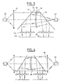
- Figure 3 shows a schematic representation of a third embodiment of an apparatus for carrying out the invention.
- separate light sources are used, which illuminate the component on its two surfaces.
- the apparatus of FIG. 3 thus has a support (not shown) for receiving an optical component 34, which has a rear surface 36 and a front surface 38.
- the apparatus furthermore has a light source having a front face. plane wave; this light source is constituted by a point source 40 and a lens 42, which generate through a semi-reflecting plate 44 a light incident on the rear surface 36 of the component to be measured with a plane wavefront.
- the light transmitted by the component is reflected by a second semi-reflecting plate 46 to a microlens array 48 and a CCD plane 50.
- the apparatus also has a light source having a spherical wavefront, which illuminates the component on the front surface.
- a second point source 52 is used, which generates through the semi-reflecting plate 46 a light incident on the front surface 38 of the component 34 with a spherical wavefront.
- the light from the source 52 and transmitted by the optical component is reflected by the semi-reflecting plate 44 to a second microlens array 54 and a second CCD plane 56.
- the apparatus clearly allows a measurement of the light transmitted by the component in two configurations.
- the component In the first configuration the component is illuminated on its surface 36 referred to as back by a light having a plane wavefront; in the second configuration, the component is illuminated on its surface 38 qualified beforehand by a light having a spherical wavefront.
- the device could of course be modified to use only one set of means for measuring the transmitted wavefront, for example using additional mirrors and semi-reflecting plates.
- Figure 4 shows a schematic representation of a fourth embodiment of an apparatus for carrying out the invention.
- the apparatus of Figure 4 differs from that of Figure 3 only in that in the second configuration a light is used. having a plane wavefront; the point source 52 of FIG. 3 is thus replaced in FIG. 4 by a point source 58 and a lens 60, which illuminate the front surface 38 of the component with a light having a plane wavefront.
- FIG. 5 shows a schematic representation of a fifth embodiment of an apparatus for carrying out the invention.
- the apparatus of FIG. 5 has the advantage of making it possible to display not only data relating to the structure of the optical component to be measured, but also the etchings on this component.
- these engravings are important for the optician: indeed, they are taken as a reference during the clipping operation, which allows the lens to be adapted to the frame shape chosen by the wearer. .
- the apparatus of FIG. 5 thus presents lighting and measuring means according to two different configurations. A CCD camera whose focus is made on the surface of the lens makes it possible to visualize the engravings.
- the apparatus therefore has a carrier (not shown) for receiving an optical component 62 having a rear surface 64 and a front surface 66.
- a CCD camera 68 is focused with a lens 70 on the surface of the camera. component.
- the axis 72 of the camera and the lens is substantially coincident with the optical axis of the component.
- the apparatus further has a light source having a plane wavefront; this light source is constituted by a point source 74 and a lens 76, which generate a light incident on the front surface 66 of the component to be measured with a plane wavefront.
- the plane wavefront light is transmitted by the component to a micro-lens array 78 and a CCD plane 80.
- the plane wavefront light is obliquely incident on the component being measured, to enable viewing the engravings of the component; more specifically, the angle ⁇ between the axis 82 of the measurement path and the axis 72 of the microetching display channel is greater than 10 °.
- the apparatus also has a light source having a spherical wavefront, which illuminates the component on the back surface.
- a second point source 84 which generates incident light on the back surface 64 of the component with a spherical wavefront, is used.
- the light from the source 84 is transmitted by the optical component to a second micro-lens array 86 and a second CCD plane 88.
- the spherical wavefront light is also obliquely incident on the component being measured, for allow to visualize the engravings of the component; more specifically, the angle ⁇ between the axis 90 of the measuring channel and the axis 72 of the microetching display channel is greater than 10 °.
- the apparatus of FIG. 5 allows a measurement of the light transmitted by the component in two configurations similar to those of FIG. 3, at the angle of incidence near. It also makes it possible to display the micro-etchings of the lenses, and thus to provide a measurement of the component in a reference linked to the micro-etchings.
- the invention proposes to determine the structure of the component. It proposes for this purpose to use an optimization search of the two surfaces of the component, using a merit function representative of the two wavefronts transmitted in the two different configurations.
- the definition of the merit function is independent of both surfaces, and in any case allows to find these two surfaces.
- the invention is based on the observation that the simultaneous operation of the two measurements makes it possible to determine the two surfaces of the component.
- the thickness of the component is not measured, it can also be determined during the search by optimization. In this case, it turns out that the merit function may have local minima for some values of the thickness, but always has an absolute minimum for the actual thickness of the component. If we know the thickness, we can simply look for the minimum for this value of the thickness. In some cases, a local optimization does not allow to find the thickness of the component; at this moment, an overall optimization makes it possible to find the extremum, and therefore the thickness of the component.
- the principle of an optimization search is known per se.
- Starting values for the front and back surfaces of the optical component are defined.
- a merit function is defined which can be calculated for current values of the front and back surfaces of the component; this merit function is designed to have a minimum or maximum value when the current values of the front and back surfaces are equal to the values at measure.
- Optimization consists of varying the current values of the front and back surfaces by successive iterations, starting from the initial values, until finding an extremum of the merit function.
- Figure 6 shows an example of a merit function definition for calculating surfaces; the explanation in the case of Figure 6 is an explanation in terms of wave fronts, for the illumination of the component on its rear surface.
- the figure shows the appearance of the optical component in reconstruction, in other words the current values of the rear surface 92 and of the front surface 94.
- the figure still shows a radius 100 recorded after transmission by the component, in one of the measurement configurations. It is possible, knowing the current values of the rear surface 92 and the front surface 94, to calculate in the space of the incident wavefront the incident beam 102 by inverse propagation through the optical component. It is thus possible to determine the intersection of the incident ray 102 with the incident wavefront 96 which is known.
- the differences of the direction cosines (x, y, z) of the radius 102 and the directional cosines (x, ⁇ , ⁇ ) of the normal 104 at the wavefront are calculated.
- the director cosine the coordinates in a coordinate system of a unitary vector colinear to the radius or normal.
- the merit function can then be expressed as the sum of the squared differences of the guiding cosines, for different radii, and for the two measurement configurations, ie: ⁇ configuration ⁇ rays ( x - x ⁇ ⁇ ) 2 + ( there - there ⁇ ⁇ ) 2 + ( z - z ⁇ ⁇ ) 2
- the function has an extremum when the values of the surfaces are equal to the real surfaces of the component.
- the merit function can be any function that quantifies the differences between the current wavefront and the reference wavefront.
- Figure 7 is similar to Figure 6 but shows the case of a reference incident wavefront which is plane.
- the normal to the incident wavefront is constant over the entire surface of the optical component; it is therefore identical for any radius 102, which simplifies calculations; indeed, it is necessary to calculate the guiding cosines of the normal at the wavefront only once. In such a configuration, it is sufficient to know the direction cosines of the beam 102, on the surface of the component illuminated by the plane wavefront light, without having to continue the inverse propagation of the beam 102.
- FIG. second radius 106 and the radius built by inverse propagation 108 are examples of the beam 102.
- the merit function is calculated from the transmission of light in the two distinct optical configurations mentioned above. Using a merit function computed from the two distinct configurations makes it possible to simultaneously determine the two surfaces of the optical component.
- the invention makes it possible to accurately determine the two surfaces of an optical component, after two measurements in transmission.
- the progressive lens measured was a glass sold by the Applicant under the Varilux Comfort brand; the back side is spherical; the front is progressive.
- the lens has a base of 7.25 diopters, a power of 5.00 diopters, a null prescription cylinder, an addition of 2.00 diopters.
- two transmission measurements were used with two plane incident wavefront lights crossing the component in opposite directions.
- the microlens array had a pitch of 2 mm, and the incident light illuminated the lens at a diameter of 50 mm; the distance between the rear face of the glass and the sensor matrix was in each direction of the 12 mm incident light.
- the optimization is done by a least squares method, on 461 variables, that is to say a modelization by Zernike polynomial with 230 variables for each surface, and a variable for the thickness. In 10 iterations, the merit function reaches a value of 0.1.10 -14 .
- the results obtained are compared with the results of a mechanical measurement of each surface of the component, using a three-dimensional measuring machine, with an accuracy better than 1 ⁇ m and a measurement step of 2 mm.
- the difference between the altitude calculated according to the invention and the measured altitude is less than 1 ⁇ m.
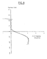
- the meridian is defined by three segments, as explained in the patents FR-A-2,683,642 and FR-A-2,683,643 of the plaintiff.
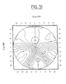
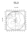
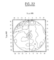
- Figures 17 to 22 are similar to Figures 8 to 13, but show the results obtained by the method of the invention. There is a very great similarity between the respective figures. In particular, we find thanks to the invention the defects of the rear face of the component, which is perfectly spherical.
- Figures 10 and 19 are quite different from Figure 16, particularly with respect to the upper part of the lens, which corresponds to the far vision area.
- the invention makes it possible to avoid deferring the defects of the rear face to the front face of the lens, when this is not exactly identical to its value. deposit.
- the meridian shown in Figure 20 corresponds well to the measured meridian shown in Figure 11. In this case, the deviations from the rear surface, supposed spherical, are small.
- the present invention is not limited to the embodiments described by way of example;
- other methods may be used to determine the wavefront of the transmitted light than Hartmann's deflectometry, and for example, a deflectometry method with fringes as in FR-A-2,710,162 or WO-A-9705467 using a Ronchi network.
- Interferometric methods can also be used.
- the method of the invention is not limited to the demonstration of small differences; the invention makes it possible to determine the corrections made by each of the two surfaces without prior assumptions on these two surfaces.
- FIG. 1 In the arrangement of FIG. 1 as in that of FIG. 2, other means can be used to generate lights with distinct wavefronts; in the embodiment of Figure 1, one could change the collimating lens 10, or add an additional lens.
- Embodiments could also be blended, and a plane wavefront light source and a spherical wavefront light source could be used in the embodiment of Figure 2. This also applies to FIGS. at 5.
- the thickness of the component in the center or at a point is known, it is possible to dispense with the means for measuring this thickness; alternatively, all known means for determining the prism or the thickness of the component may be used.
- More than two measurements may be useful for optimally determining other characteristics of the optical component.
- three sets of measurements could be used to determine the areas of the optical component and the index distribution.
- optical components from two slabs having a flat face and a non-planar face, which are assembled by their flat face.
- the invention makes it possible to determine not only the surfaces and the thickness of the component, but also the position of the interface between the two wafers.
- the incident light it is advantageous for the incident light to illuminate the whole of the useful surface of the optical component, that is to say the part of the component whose characteristics are sought.
Landscapes
- Physics & Mathematics (AREA)
- General Physics & Mathematics (AREA)
- Geometry (AREA)
- Chemical & Material Sciences (AREA)
- Analytical Chemistry (AREA)
- Testing Of Optical Devices Or Fibers (AREA)
- Length Measuring Devices By Optical Means (AREA)
Claims (23)
- Verfahren zum Messen beim Übertragen der geometrischen Struktur eines optischen Bauteils (2) mit den folgenden Schritten:- Beleuchten des optischen Bauteils durch ein erstes einfallendes Licht (8, 10), dessen Wellenfront bekannt ist,- Messen (16, 18) der Wellenfront des ersten Lichts nach Übertragen durch den optischen Bauteil,- Beleuchten des optischen Bauteils durch ein zweites einfallendes Licht (12, 14), dessen Wellenfront bekannt ist,- Messen (16, 18) der Wellenfront des zweiten Lichts nach Übertragen durch den optischen Bauteil,- Berechnen der geometrischen Struktur des optischen Bauteils ausgehend von den bei den Messschritten gemessenen Wellenfronten.
- Verfahren nach Anspruch 1, dadurch gekennzeichnet, dass die Wellenfronten auf der Seite der gleichen Fläche des Bauteils bei den verschiedenen Messschritten unterschiedlich sind.
- Verfahren nach Anspruch 1 oder 2, dadurch gekennzeichnet, dass der Messschritt durch Hartmann- oder Shack-Hartmann-Deflektometrie ausgeführt wird.
- Verfahren nach Anspruch 1 oder 2, dadurch gekennzeichnet, dass der Messschritt durch Randdeflektometrie ausgeführt wird.
- Verfahren nach Anspruch 1 oder 2, dadurch gekennzeichnet, dass der Messschritt ein Messschritt durch Interferometrie ist.
- Verfahren nach einem der Ansprüche 1 bis 5, dadurch gekennzeichnet, dass die Beleuchtungsschritte das Beleuchten des Bauteils auf einer seiner Flächen und das Beleuchten des Bauteils auf der anderen seiner Flächen aufweisen.
- Verfahren nach Anspruch 6, dadurch gekennzeichnet, dass das erste und das zweite Licht identische Wellenfronten aufweisen.
- Verfahren nach Anspruch 7, dadurch gekennzeichnet, dass die Beleuchtungsschritte das Beleuchten des optischen Bauteils durch ein gleiches einfallendes Licht aufweisen, und dass das Verfahren einen Umdrehschritt des optischen Bauteils aufweist.
- Verfahren nach einem der Ansprüche 1 bis 5, dadurch gekennzeichnet, dass die Beleuchtungsschritte das Beleuchten des Bauteils auf einer seiner Flächen aufweisen.
- Verfahren nach Anspruch 9, dadurch gekennzeichnet, dass das erste und das zweite Licht unterschiedliche Wellenfronten aufweisen.
- Verfahren nach einem der vorhergehenden Ansprüche, dadurch gekennzeichnet, dass der Berechnungsschritt durch Optimieren einer Leistungsfunktion erfolgt, die ausgehend von mindestens zwei Messschritten berechnet wird.
- Verfahren nach einem der vorhergehenden Ansprüche, gekennzeichnet durch einen Schritt des Messens der Stärke des Bauteils in mindestens einem Punkt.
- Verfahren nach einem der vorhergehenden Ansprüche, gekennzeichnet durch die folgenden Schritte:- Beleuchten des optischen Bauteils durch ein drittes einfallendes Licht, dessen Wellenfront bekannt ist,- Messen der Wellenfront des dritten Lichts nach Übertragen durch den optischen Bauteil.
- Gerät zum Messen beim Übertragen der geometrischen Struktur eines optischen Bauteils (2), umfassend:- Mittel (8, 10) zum Beleuchten des optischen Bauteils durch ein erstes einfallendes Licht, dessen Wellenfront bekannt ist,- Mittel zum Messen (16, 18) der Wellenfront des ersten Lichts nach dem Übertragen durch den optischen Bauteil,- Mittel zum Beleuchten (12, 14) des optischen Bauteils durch ein zweites einfallendes Licht, dessen Wellenfront bekannt und unterschiedlich ist,- Mittel zum Messen (16, 18) der Wellenfront des zweiten Lichts nach dem Übertragen durch den optischen Bauteil,- Mittel zum Berechnen der geometrischen Struktur des optischen Bauteils ausgehend von Wellenfronten, die bei den Messschritten gemessen wurden.
- Gerät nach Anspruch 14, dadurch gekennzeichnet, dass die Messmittel eine Mikronlinsen-Matrix (16) aufweisen.
- Gerät nach Anspruch 14, dadurch gekennzeichnet, dass die Messmittel ein Gitter aufweisen.
- Gerät des Anspruchs 14, 15 oder 16, dadurch gekennzeichnet, dass die Mittel zum Beleuchten des optischen Bauteils durch ein erstes einfallendes Licht und die Mittel zum Beleuchten des optischen Bauteils durch ein zweites einfallendes Licht jeweils den Bauteil auf einer seiner Flächen beleuchten.
- Gerät nach Anspruch 17, dadurch gekennzeichnet, dass das erste und das zweite Licht identische Wellenfronten aufweisen.
- Gerät nach Anspruch 14, 15 oder 16, dadurch gekennzeichnet, dass die Mittel zum Beleuchten des optischen Bauteils durch ein erstes einfallendes Licht und die Mittel zum Beleuchten des optischen Bauteils durch ein zweites einfallendes Licht die gleiche Fläche des Bauteils beleuchten.
- Gerät nach Anspruch 19, dadurch gekennzeichnet, dass das erste und das zweite Licht unterschiedliche Wellenfronten aufweisen.
- Gerät nach einem der Ansprüche 14 bis 20, gekennzeichnet durch Mittel zum Messen der Stärke des Bauteils.
- Gerät nach einem der Ansprüche 14 bis 21, gekennzeichnet durch- Mittel zum Beleuchten des optischen Bauteils durch ein drittes einfallendes Licht, dessen Wellenfront bekannt ist,- Mittel zum Messen der Wellenfront des dritten Lichts nach dem Übertragen durch den optischen Bauteil.
- Gerät nach einem der Ansprüche 14 bis 22, gekennzeichnet durch Mittel (68, 70) zum Anzeigen von Mikrogravuren auf dem Bauteil.
Applications Claiming Priority (3)
| Application Number | Priority Date | Filing Date | Title |
|---|---|---|---|
| FR0010794A FR2813391B1 (fr) | 2000-08-22 | 2000-08-22 | Procede et appareil de mesure en transmission de la structure geometrique d'un composant optique |
| FR0010794 | 2000-08-22 | ||
| PCT/FR2001/002626 WO2002016902A1 (fr) | 2000-08-22 | 2001-08-17 | Procede et appareil de mesure en transmission de la structure geometrique d'un composant optique |
Publications (2)
| Publication Number | Publication Date |
|---|---|
| EP1224448A1 EP1224448A1 (de) | 2002-07-24 |
| EP1224448B1 true EP1224448B1 (de) | 2008-01-23 |
Family
ID=8853640
Family Applications (1)
| Application Number | Title | Priority Date | Filing Date |
|---|---|---|---|
| EP01965331A Expired - Lifetime EP1224448B1 (de) | 2000-08-22 | 2001-08-17 | Verfahren und apparat zur messung der geometrischen struktur eines optischen bauteils durch lichtübertragung |
Country Status (8)
| Country | Link |
|---|---|
| US (1) | US6909498B2 (de) |
| EP (1) | EP1224448B1 (de) |
| JP (1) | JP5173106B2 (de) |
| AT (1) | ATE384940T1 (de) |
| DE (1) | DE60132551T2 (de) |
| ES (1) | ES2300355T3 (de) |
| FR (1) | FR2813391B1 (de) |
| WO (1) | WO2002016902A1 (de) |
Cited By (1)
| Publication number | Priority date | Publication date | Assignee | Title |
|---|---|---|---|---|
| DE112014004645B4 (de) * | 2013-10-08 | 2025-12-04 | Emage Vision Pte. Ltd. | System und Verfahren zur Inspektion feuchter Kontaktlinsen |
Families Citing this family (18)
| Publication number | Priority date | Publication date | Assignee | Title |
|---|---|---|---|---|
| DE10348509A1 (de) * | 2003-10-18 | 2005-05-19 | Carl Zeiss Jena Gmbh | Wellenfrontsensor |
| GB0402941D0 (en) * | 2004-02-11 | 2004-03-17 | Qinetiq Ltd | Surface shape measurement |
| FR2866718B1 (fr) * | 2004-02-24 | 2006-05-05 | Essilor Int | Dispositif centreur-bloqueur d'une lentille ophtalmique de lunettes, methode de detection automatique et methodes de centrage manuel associees |
| FR2866719B1 (fr) * | 2004-02-24 | 2006-05-19 | Essilor Int | Methode de contrage manuel d'une lentille ophtalmique de lunettes dans un centreur-bloqueur et dispositif centreur-bloqueur associe |
| FR2879736B1 (fr) * | 2004-12-20 | 2007-02-02 | Essilor Int | Procede et dispositif de mesure sans contact de la courbure d'un objet ophtalmique |
| FR2880118B1 (fr) * | 2004-12-23 | 2007-03-02 | Essilor Int | Procede et appareil de mesure locale des caracteristiques de refraction d'une lentille en un ou plusieurs points specifiques de cette lentille |
| JP4683270B2 (ja) * | 2005-03-30 | 2011-05-18 | 株式会社ニデック | レンズメータ |
| US20060232766A1 (en) * | 2005-03-31 | 2006-10-19 | Watterson Robert J Jr | Methods of inspecting ophthalmic lenses |
| US7583389B2 (en) * | 2006-04-07 | 2009-09-01 | Amo Wavefront Sciences, Llc | Geometric measurement system and method of measuring a geometric characteristic of an object |
| US20130201474A1 (en) * | 2012-02-07 | 2013-08-08 | Bausch & Lomb Incorporated | Aberrometer for Measuring Parameters of a Lens Using Multiple Point Sources of Light |
| EP2637011A1 (de) | 2012-03-09 | 2013-09-11 | Essilor International | Verfahren und Vorrichtung zur Messung der geometrischen Struktur einer optischen Komponente |
| EP2880398B1 (de) | 2012-07-31 | 2018-03-28 | Essilor International | Verfahren und system zur identifizierung einer gegebenen geometrischen eigenschaft einer optischen komponente |
| DE102012019110B4 (de) * | 2012-09-28 | 2017-05-11 | Bundesrepublik Deutschland, endvertreten durch die Physikalisch-Technische Bundesanstalt (PTB) | Topographiemessverfahren und Topographiemessvorrichtung |
| JP6279712B2 (ja) * | 2013-05-02 | 2018-02-14 | カール ツァイス ヴィジョン インターナショナル ゲーエムベーハー | 物体の空間構造を求める方法及びシステム |
| DE102013219838B4 (de) * | 2013-09-30 | 2015-11-26 | Carl Zeiss Ag | Verfahren und System für das Ermitteln der räumlichen Struktur eines Gegenstands |
| DE102018001385A1 (de) * | 2018-02-21 | 2019-08-22 | Schneider Gmbh & Co. Kg | Vorrichtung und Verfahren zum Vermessen mindestens eines optisch wirksamen Gegenstands |
| EP3531067B1 (de) | 2018-02-21 | 2025-04-02 | Schneider GmbH & Co. KG | Vorrichtung und verfahren zum vermessen mindestens eines optisch wirksamen gegenstands |
| DE102024126197A1 (de) * | 2024-09-12 | 2026-03-12 | Schott Ag | Verfahren und Vorrichtung zur Prüfung optischer Verbundelemente |
Family Cites Families (12)
| Publication number | Priority date | Publication date | Assignee | Title |
|---|---|---|---|---|
| JP2698362B2 (ja) * | 1987-12-09 | 1998-01-19 | 株式会社トプコン | 被測定物の透過波面の形状測定方法及びその方法に用いる装置 |
| JPH0611323A (ja) * | 1992-06-26 | 1994-01-21 | Minolta Camera Co Ltd | 形状測定装置 |
| DE69402281T2 (de) * | 1993-09-17 | 1997-09-04 | Essilor Int | Verfahren und Gerät zur absoluten Messung der geometrischen oder optischen Struktur eines optischen Bestandteiles |
| EP0765468B1 (de) * | 1994-06-14 | 2002-10-23 | Visionix Ltd. | Apparat zur topometrischen erfassung eines optischen elementes |
| FR2737568B1 (fr) * | 1995-08-02 | 1997-09-26 | Essilor Int | Appareil et procede de deflectometrie a franges |
| US6043885A (en) * | 1996-07-12 | 2000-03-28 | Essilor International | Fringe deflectometry apparatus and method |
| JPH1114498A (ja) * | 1997-06-26 | 1999-01-22 | Canon Inc | 光学系、測定方法及び装置 |
| US6072570A (en) * | 1997-07-24 | 2000-06-06 | Innotech | Image quality mapper for progressive eyeglasses |
| JPH11237311A (ja) * | 1998-02-23 | 1999-08-31 | Canon Inc | 波面測定方法及び波面測定装置 |
| NL1009366C2 (nl) * | 1998-06-10 | 1999-12-13 | Stichting Tech Wetenschapp | Interferometer. |
| JP2000065684A (ja) * | 1998-08-17 | 2000-03-03 | Ricoh Co Ltd | 屈折率分布の測定方法及び装置 |
| US6750958B1 (en) * | 1999-06-09 | 2004-06-15 | Optikos Corporation | Automated optical measurement apparatus and method |
-
2000
- 2000-08-22 FR FR0010794A patent/FR2813391B1/fr not_active Expired - Fee Related
-
2001
- 2001-08-17 DE DE60132551T patent/DE60132551T2/de not_active Expired - Lifetime
- 2001-08-17 AT AT01965331T patent/ATE384940T1/de not_active IP Right Cessation
- 2001-08-17 WO PCT/FR2001/002626 patent/WO2002016902A1/fr not_active Ceased
- 2001-08-17 US US10/110,152 patent/US6909498B2/en not_active Expired - Lifetime
- 2001-08-17 JP JP2002521949A patent/JP5173106B2/ja not_active Expired - Fee Related
- 2001-08-17 ES ES01965331T patent/ES2300355T3/es not_active Expired - Lifetime
- 2001-08-17 EP EP01965331A patent/EP1224448B1/de not_active Expired - Lifetime
Cited By (1)
| Publication number | Priority date | Publication date | Assignee | Title |
|---|---|---|---|---|
| DE112014004645B4 (de) * | 2013-10-08 | 2025-12-04 | Emage Vision Pte. Ltd. | System und Verfahren zur Inspektion feuchter Kontaktlinsen |
Also Published As
| Publication number | Publication date |
|---|---|
| JP5173106B2 (ja) | 2013-03-27 |
| FR2813391B1 (fr) | 2002-11-29 |
| US6909498B2 (en) | 2005-06-21 |
| ATE384940T1 (de) | 2008-02-15 |
| ES2300355T3 (es) | 2008-06-16 |
| EP1224448A1 (de) | 2002-07-24 |
| JP2004507730A (ja) | 2004-03-11 |
| DE60132551D1 (de) | 2008-03-13 |
| US20030112426A1 (en) | 2003-06-19 |
| WO2002016902A1 (fr) | 2002-02-28 |
| FR2813391A1 (fr) | 2002-03-01 |
| DE60132551T2 (de) | 2009-01-22 |
Similar Documents
| Publication | Publication Date | Title |
|---|---|---|
| EP0644411B1 (de) | Verfahren und Gerät zur absoluten Messung der geometrischen oder optischen Struktur eines optischen Bestandteiles | |
| EP1224448A1 (de) | Verfahren und apparat zur messung der geometrischen struktur eines optischen bauteils durch lichtübertragung | |
| EP0290347B1 (de) | Hochleistungsleuchte, insbesondere für Kraftfahrzeuge | |
| EP2646789B9 (de) | Verfahren zur bestimmung von mindestens einer refraktionseigenschaft einer ophthalmischen linse | |
| EP2095069A2 (de) | Elektronisches optisches verfahren zur 3d-messung eines objekts durch randprojektion und verwendung eines phasenverschiebungsverfahrens sowie entsprechendes system | |
| EP2872871B1 (de) | Verfahren und system zur rekonstruktion der optischen eigenschaften von in einem flüssigmedium gebadeten, lichtbrechenden objekten | |
| EP0538126B1 (de) | Verfahren und Vorrichtung zur Analyse einer Lichtwellenfront | |
| FR2768814A1 (fr) | Procede et dispositif optiques d'analyse de surface d'onde | |
| FR3010182A1 (fr) | Methode et dispositif de determination de la position et de l'orientation d'une surface speculaire formant un dioptre | |
| EP1157261A2 (de) | Verfahren und vorrichtung zur analyse einer hochdynamischen wellenfront | |
| CA2701151A1 (fr) | Systeme d'imagerie a modification de front d'onde et procede d'augmentation de la profondeur de champ d'un systeme d'imagerie | |
| EP0840158B1 (de) | Vorrichtung zur Bestimmung von Phasenfehlern elektromagnetischer Wellen | |
| EP2823279B1 (de) | Verfahren und vorrichtung zur messung der geometrischen struktur einer optischen komponente | |
| WO2008023024A1 (fr) | Procede de mesure sans contact d'objets tridimensionnels a deux couches par ombroscopie optique a une seule vue | |
| EP3785083B1 (de) | Verfahren zur verarbeitung eines hologramms, zugehörige vorrichtung, holografisches anzeigesystem und computerprogramm | |
| EP0069071B1 (de) | Identifikationsverfahren eines Objekts und Messung seiner Rotation und seiner Orientation und Vorrichtung zur Ausführung dieses Verfahrens | |
| EP0842409B1 (de) | Gerät und verfahren zur streifen-ablenkungsmessung | |
| FR2606522A1 (fr) | Dispositif et procede optique de mise au point photoelectrique, notamment pour microscopes d'operations chirurgicales | |
| EP3899458B1 (de) | Instrument mit mehreren optischen kanälen | |
| EP3835748A1 (de) | Kontrollsystem mindestens einer komponente eines optischen elements | |
| FR3026227A1 (fr) | Dispositif d'acquisition d'images 3d | |
| EP2677368A1 (de) | Vorrichtung und Verfahren zum Lesen eines synthetischen Hologramms | |
| FR2907214A1 (fr) | "procede de correction d'un analyseur de front d'onde,et analyseur implementant ce procede" | |
| FR2710162A1 (fr) | Procédé de mesure absolue de la structure géométrique ou optique d'un composant optique et dispositif pour sa mise en Óoeuvre. | |
| FR3155061A1 (fr) | Appareil et procédé de micro-spectrométrie Raman confocal avec système de mise au point |
Legal Events
| Date | Code | Title | Description |
|---|---|---|---|
| PUAI | Public reference made under article 153(3) epc to a published international application that has entered the european phase |
Free format text: ORIGINAL CODE: 0009012 |
|
| AK | Designated contracting states |
Kind code of ref document: A1 Designated state(s): AT BE CH CY DE DK ES FI FR GB GR IE IT LI LU MC NL PT SE TR |
|
| 17P | Request for examination filed |
Effective date: 20030324 |
|
| RIN1 | Information on inventor provided before grant (corrected) |
Inventor name: LE SAUX, GILLES Inventor name: BELL, FRANCIS Inventor name: DEVIE, PIERRE |
|
| GRAP | Despatch of communication of intention to grant a patent |
Free format text: ORIGINAL CODE: EPIDOSNIGR1 |
|
| GRAS | Grant fee paid |
Free format text: ORIGINAL CODE: EPIDOSNIGR3 |
|
| GRAA | (expected) grant |
Free format text: ORIGINAL CODE: 0009210 |
|
| AK | Designated contracting states |
Kind code of ref document: B1 Designated state(s): AT BE CH CY DE DK ES FI FR GB GR IE IT LI LU MC NL PT SE TR |
|
| REG | Reference to a national code |
Ref country code: GB Ref legal event code: FG4D Free format text: NOT ENGLISH |
|
| REG | Reference to a national code |
Ref country code: CH Ref legal event code: EP |
|
| REG | Reference to a national code |
Ref country code: IE Ref legal event code: FG4D Free format text: LANGUAGE OF EP DOCUMENT: FRENCH |
|
| REF | Corresponds to: |
Ref document number: 60132551 Country of ref document: DE Date of ref document: 20080313 Kind code of ref document: P |
|
| GBT | Gb: translation of ep patent filed (gb section 77(6)(a)/1977) |
Effective date: 20080227 |
|
| REG | Reference to a national code |
Ref country code: CH Ref legal event code: NV Representative=s name: ZIMMERLI, WAGNER & PARTNER AG |
|
| REG | Reference to a national code |
Ref country code: ES Ref legal event code: FG2A Ref document number: 2300355 Country of ref document: ES Kind code of ref document: T3 |
|
| NLV1 | Nl: lapsed or annulled due to failure to fulfill the requirements of art. 29p and 29m of the patents act | ||
| PG25 | Lapsed in a contracting state [announced via postgrant information from national office to epo] |
Ref country code: FI Free format text: LAPSE BECAUSE OF FAILURE TO SUBMIT A TRANSLATION OF THE DESCRIPTION OR TO PAY THE FEE WITHIN THE PRESCRIBED TIME-LIMIT Effective date: 20080123 |
|
| PG25 | Lapsed in a contracting state [announced via postgrant information from national office to epo] |
Ref country code: AT Free format text: LAPSE BECAUSE OF FAILURE TO SUBMIT A TRANSLATION OF THE DESCRIPTION OR TO PAY THE FEE WITHIN THE PRESCRIBED TIME-LIMIT Effective date: 20080123 |
|
| PG25 | Lapsed in a contracting state [announced via postgrant information from national office to epo] |
Ref country code: PT Free format text: LAPSE BECAUSE OF FAILURE TO SUBMIT A TRANSLATION OF THE DESCRIPTION OR TO PAY THE FEE WITHIN THE PRESCRIBED TIME-LIMIT Effective date: 20080623 |
|
| REG | Reference to a national code |
Ref country code: IE Ref legal event code: FD4D |
|
| PG25 | Lapsed in a contracting state [announced via postgrant information from national office to epo] |
Ref country code: NL Free format text: LAPSE BECAUSE OF FAILURE TO SUBMIT A TRANSLATION OF THE DESCRIPTION OR TO PAY THE FEE WITHIN THE PRESCRIBED TIME-LIMIT Effective date: 20080123 Ref country code: SE Free format text: LAPSE BECAUSE OF FAILURE TO SUBMIT A TRANSLATION OF THE DESCRIPTION OR TO PAY THE FEE WITHIN THE PRESCRIBED TIME-LIMIT Effective date: 20080423 Ref country code: DK Free format text: LAPSE BECAUSE OF FAILURE TO SUBMIT A TRANSLATION OF THE DESCRIPTION OR TO PAY THE FEE WITHIN THE PRESCRIBED TIME-LIMIT Effective date: 20080123 Ref country code: IE Free format text: LAPSE BECAUSE OF FAILURE TO SUBMIT A TRANSLATION OF THE DESCRIPTION OR TO PAY THE FEE WITHIN THE PRESCRIBED TIME-LIMIT Effective date: 20080123 |
|
| PGFP | Annual fee paid to national office [announced via postgrant information from national office to epo] |
Ref country code: CH Payment date: 20080826 Year of fee payment: 8 Ref country code: ES Payment date: 20080924 Year of fee payment: 8 |
|
| PLBE | No opposition filed within time limit |
Free format text: ORIGINAL CODE: 0009261 |
|
| STAA | Information on the status of an ep patent application or granted ep patent |
Free format text: STATUS: NO OPPOSITION FILED WITHIN TIME LIMIT |
|
| 26N | No opposition filed |
Effective date: 20081024 |
|
| PGFP | Annual fee paid to national office [announced via postgrant information from national office to epo] |
Ref country code: BE Payment date: 20080829 Year of fee payment: 8 |
|
| PG25 | Lapsed in a contracting state [announced via postgrant information from national office to epo] |
Ref country code: MC Free format text: LAPSE BECAUSE OF NON-PAYMENT OF DUE FEES Effective date: 20080831 |
|
| PG25 | Lapsed in a contracting state [announced via postgrant information from national office to epo] |
Ref country code: CY Free format text: LAPSE BECAUSE OF FAILURE TO SUBMIT A TRANSLATION OF THE DESCRIPTION OR TO PAY THE FEE WITHIN THE PRESCRIBED TIME-LIMIT Effective date: 20080123 |
|
| PG25 | Lapsed in a contracting state [announced via postgrant information from national office to epo] |
Ref country code: IT Free format text: LAPSE BECAUSE OF FAILURE TO SUBMIT A TRANSLATION OF THE DESCRIPTION OR TO PAY THE FEE WITHIN THE PRESCRIBED TIME-LIMIT Effective date: 20080123 |
|
| REG | Reference to a national code |
Ref country code: CH Ref legal event code: PFA Owner name: ESSILOR INTERNATIONAL COMPAGNIE GENERALE D'OPTIQU Free format text: ESSILOR INTERNATIONAL COMPAGNIE GENERALE D'OPTIQUE#147, RUE DE PARIS#94227 CHARENTON CEDEX (FR) -TRANSFER TO- ESSILOR INTERNATIONAL COMPAGNIE GENERALE D'OPTIQUE#147, RUE DE PARIS#94227 CHARENTON CEDEX (FR) |
|
| BERE | Be: lapsed |
Owner name: ESSILOR INTERNATIONAL CIE GENERALE D'OPTIQUE Effective date: 20090831 |
|
| REG | Reference to a national code |
Ref country code: CH Ref legal event code: PL |
|
| PG25 | Lapsed in a contracting state [announced via postgrant information from national office to epo] |
Ref country code: CH Free format text: LAPSE BECAUSE OF NON-PAYMENT OF DUE FEES Effective date: 20090831 Ref country code: LI Free format text: LAPSE BECAUSE OF NON-PAYMENT OF DUE FEES Effective date: 20090831 |
|
| PG25 | Lapsed in a contracting state [announced via postgrant information from national office to epo] |
Ref country code: BE Free format text: LAPSE BECAUSE OF NON-PAYMENT OF DUE FEES Effective date: 20090831 |
|
| PG25 | Lapsed in a contracting state [announced via postgrant information from national office to epo] |
Ref country code: LU Free format text: LAPSE BECAUSE OF NON-PAYMENT OF DUE FEES Effective date: 20080817 |
|
| PG25 | Lapsed in a contracting state [announced via postgrant information from national office to epo] |
Ref country code: TR Free format text: LAPSE BECAUSE OF FAILURE TO SUBMIT A TRANSLATION OF THE DESCRIPTION OR TO PAY THE FEE WITHIN THE PRESCRIBED TIME-LIMIT Effective date: 20080123 |
|
| REG | Reference to a national code |
Ref country code: ES Ref legal event code: FD2A Effective date: 20090818 |
|
| PG25 | Lapsed in a contracting state [announced via postgrant information from national office to epo] |
Ref country code: GR Free format text: LAPSE BECAUSE OF FAILURE TO SUBMIT A TRANSLATION OF THE DESCRIPTION OR TO PAY THE FEE WITHIN THE PRESCRIBED TIME-LIMIT Effective date: 20080424 |
|
| PG25 | Lapsed in a contracting state [announced via postgrant information from national office to epo] |
Ref country code: ES Free format text: LAPSE BECAUSE OF NON-PAYMENT OF DUE FEES Effective date: 20090818 |
|
| REG | Reference to a national code |
Ref country code: FR Ref legal event code: PLFP Year of fee payment: 16 |
|
| REG | Reference to a national code |
Ref country code: FR Ref legal event code: PLFP Year of fee payment: 17 |
|
| REG | Reference to a national code |
Ref country code: DE Ref legal event code: R082 Ref document number: 60132551 Country of ref document: DE Representative=s name: 24IP LAW GROUP SONNENBERG FORTMANN, DE Ref country code: DE Ref legal event code: R081 Ref document number: 60132551 Country of ref document: DE Owner name: ESSILOR INTERNATIONAL, FR Free format text: FORMER OWNER: ESSILOR INTERNATIONAL COMPAGNIE GENERALE D'OPTIQUE, CHARENTON, FR |
|
| REG | Reference to a national code |
Ref country code: GB Ref legal event code: 732E Free format text: REGISTERED BETWEEN 20180517 AND 20180523 |
|
| REG | Reference to a national code |
Ref country code: FR Ref legal event code: TP Owner name: ESSILOR INTERNATIONAL, FR Effective date: 20180601 |
|
| REG | Reference to a national code |
Ref country code: FR Ref legal event code: PLFP Year of fee payment: 18 |
|
| PGFP | Annual fee paid to national office [announced via postgrant information from national office to epo] |
Ref country code: DE Payment date: 20200827 Year of fee payment: 20 Ref country code: GB Payment date: 20200827 Year of fee payment: 20 Ref country code: FR Payment date: 20200825 Year of fee payment: 20 |
|
| REG | Reference to a national code |
Ref country code: DE Ref legal event code: R071 Ref document number: 60132551 Country of ref document: DE |
|
| REG | Reference to a national code |
Ref country code: GB Ref legal event code: PE20 Expiry date: 20210816 |
|
| PG25 | Lapsed in a contracting state [announced via postgrant information from national office to epo] |
Ref country code: GB Free format text: LAPSE BECAUSE OF EXPIRATION OF PROTECTION Effective date: 20210816 |
|
| P01 | Opt-out of the competence of the unified patent court (upc) registered |
Effective date: 20230525 |