EP1224720B1 - Vereinfachte stromaufteilungsschaltung - Google Patents
Vereinfachte stromaufteilungsschaltung Download PDFInfo
- Publication number
- EP1224720B1 EP1224720B1 EP00991880.6A EP00991880A EP1224720B1 EP 1224720 B1 EP1224720 B1 EP 1224720B1 EP 00991880 A EP00991880 A EP 00991880A EP 1224720 B1 EP1224720 B1 EP 1224720B1
- Authority
- EP
- European Patent Office
- Prior art keywords
- terminal
- set point
- current sharing
- coupled
- voltage
- Prior art date
- Legal status (The legal status is an assumption and is not a legal conclusion. Google has not performed a legal analysis and makes no representation as to the accuracy of the status listed.)
- Expired - Lifetime
Links
Images



Classifications
-
- H—ELECTRICITY
- H02—GENERATION; CONVERSION OR DISTRIBUTION OF ELECTRIC POWER
- H02J—ELECTRIC POWER NETWORKS; CIRCUIT ARRANGEMENTS OR SYSTEMS FOR SUPPLYING OR DISTRIBUTING ELECTRIC POWER; SYSTEMS FOR STORING ELECTRIC ENERGY
- H02J1/00—Circuit arrangements for DC mains or DC distribution networks
- H02J1/10—Parallel operation of DC sources
- H02J1/102—Parallel operation of DC sources being switching converters
Definitions
- This invention relates generally to logic integrated circuits, and more particularly to a simplified logic integrated circuit for current sharing for a DC-to-DC power module without internal current share circuitry.
- the first solution is the droop method. In this method the system output voltage is allowed to droop as the load current increases, resulting in improved current sharing. The droop method works well if the initial set point of the different modules is relatively similar. However, there are systems which do not permit the voltage to droop.
- the second solution, active current sharing is generally used in these systems. In active current sharing, the individual current of each parallel module is measured, amplified, and compared to each other. Based on the result of this comparison, the module set point is adjusted to drive the difference between the output currents of each module to zero.
- active current sharing requires the use of several operational amplifiers.
- US 5 724 237 A relates to an apparatus for sharing a load current among frequency-controlled DC-DC converters.
- the load current delivered by such converters typically varies approximately proportionately with the converter operating frequency.
- a frequency to voltage converter senses the operating frequency and converts it to a filtered analogue voltage which is functionally related to the input frequency.
- An amplifier circuit compares this analogue signal with the same signal from other DC-DC converters.
- the error signal is used as a control signal to adjust the converter output voltage to force the analogue signal to be substantially equal to the analogue signals from other DC-DC converters.
- the present invention achieves technical advantages as a simplified current share circuit scheme for multiple power modules.
- the invention provides cost efficient and less complex circuitry than the prior art.
- the present invention may be adapted for use with power modules which are not designed for current sharing.
- the current sharing circuit scheme comprises a first and second power module.
- Each module includes an input side and an output side with the power modules coupled to each other via respective input sides.
- Each of the output sides includes a positive terminal and a negative terminal.
- the circuit scheme also comprises first and second circuit output voltage terminals and first and second set point controls coupled to the negative terminal of each of the output sides.
- a first and second initial set point control is included providing current signal paths between the corresponding first and second set point controls and the first output voltage terminal.
- the first and second set point and the first and second initial set point controls are configured to allow current sharing through said first and second output voltage terminal when a current signal is applied to said input side of said first and second power modules.
- the embodiment of the present invention as set forth above, may be adapted to more precisely handle the variations in the output voltage.
- Regulation terminals are coupled between the first and second power modules and the negative terminal of said circuit output voltage terminal to maintain the initial set point of the first and second power modules.
- Regulation terminals are also added between the first and second power module output sides and the other module's trim terminal such that the voltage across the first output terminal is controlled relative to the voltage across the circuit output voltage terminal to facilitate current sharing.
- the present invention may be adapted to facilitate current sharing between three power modules.
- Various embodiments are also included to facilitate current sharing under conditions including mismatched system impedances.
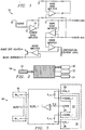
- FIG. 1 A typical implementation of a circuit 10 used for active current sharing is shown in Figure 1 .
- the circuit 10 is utilized for active current sharing between a plurality of power modules16 (shown in figure 2 ).
- the current supplied by each of a plurality of power modules16 is measured in the sense resistor Rsense.
- This signal is amplified in the current sense amplifier 14.
- a signal proportional to the sense current is developed across the current share bus represented by "share + bus” and "share - bus”, compared to the signal coming from the other power modules 16, and, finally, adjustment is made depending on whether the current being delivered by the module is high or low.
- the adjusting signal is usually injected into the voltage loop of the power module 16 so as to adjust its regulation point. This is a very elegant solution to the problem.
- Many different variations of active current sharing have been suggested and implemented in industry and may be used with DC-to-DC power modules 16.
- a typical power module 16 that may be used in a current share circuit is shown in Figure 2 .
- the power module 16 comprises an input terminal 18, output terminal 20, a voltage sense terminal 22, and a trim terminal 24.
- the current enters the power module 16 through the input terminal 18 and is measured and amplified as necessary.
- the difference between the output and voltage sense terminals 20 and 22 can be used to provide information regarding the load current. This information is used, in turn, to adjust the trim terminal 24 which controls the voltage across the output terminal 20.
- this configuration allows for the current of a power module 16 to be compared to that of another module.
- the result is a system of two or more power modules 16 current sharing.
- the input and output terminal 18 and 20, respectively are pins which are used to integrate the power module 16 into the current share circuit.
- An on/off pin is also included to turn the power module on and off.
- the voltage sense terminal 22 and trim terminal 24 are also pins.
- the voltage sense terminal 22 comprises a positive and negative sub-terminal 26 and 28, respectively.
- the voltage sense terminal 22 positive and negative sub-terminals 26 and 28 allow the power module 16 to regulate the correct system voltage. This is accomplished by providing the load current information to the trim pin 34 which is used to adjust the output voltage of the power module 16.
- the output voltage of the power module 16 and the regulated system voltage are not the same. The difference between these two voltages varies depending on the load current. The larger the load current the greater the difference between these two voltages.
- the output voltage of the power module 16 is always greater than the regulated system voltage.
- a positive signal into the trim pin 34 adjusts the output voltage of the module to a higher voltage relative to its initial set point.
- a negative signal into the trim terminal adjusts the output voltage to a lower voltage.
- the present invention a simplified current share circuitry, utilizes power module 16 to minimize system cost without degrading the performance of the current share system.
- Current sharing within 10 % can be easily obtained.
- the present invention does away with the current share bus as shown in Figure 1 or any additional op-amps.
- this current share technique can be implemented in existing DC-to-DC power modules 16 that are not designed for current sharing.
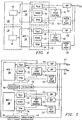
- Figure 4 is one embodiment of the present invention having a first and a second power module, 36 and 38, respectively.
- the first and second power modules comprise an input side 30 and an output side 32.
- the first and second modules 36 and 38 are coupled together via the respective input sides 30 utilizing the input terminals 18 included in the input side 30.
- the output sides 32 are comprised of the output, voltage sense, and trim terminals 20, 22, and 24, respectively, which are used to facilitate current sharing between the first and second power modules 36 and 38.
- the voltage sense terminal 22 provides information regarding the load current. Therefore, this information can be used accordingly to adjust the trim terminal 24 on each of the first and second power modules 36 and 38 to force the power modules 36 and 38 to current share.
- Set point controls 40 and 41 are implemented and coupled to each of the power modules 36 and 38, respectively, to overcome the difference in the output voltage set points of the power modules 36 and 38.
- the initial set point of each power module 36 and 38 will be maintained by an initial set point controls 42 and 45.
- the natural impedance, indicated by 43, that exists between the output terminal 20 of the power module 16 and the place at which the system voltage is regulated is used as a current sense resistor.
- first and second power modules 36 and 38 will current share by what is known as the droop method. As the two module system requires more current, the system voltage will droop. In some applications, a 100 to 200 mV variation in the output voltage is not a problem and the embodiment, as set forth, is more than adequate. In most applications, however, precise regulation of the output voltage is required and a 20 to 200 mV variation in the output voltage can not be tolerated.
- a second embodiment of the present invention is shown in Figure 5 .
- This embodiment provides the precise regulation of the output voltage that is required in some applications.
- a first and third regulation terminal 43 and 44 are included in the second embodiment and are coupled between the trim terminal 24 of the first and second power modules 36 and 38, respectively, and the second output voltage terminal 46.
- Second and fourth regulation terminals 48 and 49, respectively, must also be implemented between the trim terminal 24 of the first power module 36 and the output terminal 20 of the second power module 38 and between the trim terminal 24 of the second power module 38 and the output terminal 20 of the first power module 36.
- the second and fourth regulation terminals 48 and 49 will facilitate regulating the voltages such that the first and second power modules 36 and 38 will current share.
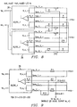
- FIG. 6 A circuit diagram of the present invention combining both embodiments is shown in Figure 6 .
- the load increases the voltage measured at the output terminals 20 of the first and second power modules 36 and 38 will increase relative to the regulated system voltage.
- the positive output voltage terminal (Vo_I1_+ and Vo_I2_+) of each power module 36 and 38 will increase relative to the positive system output voltage (Vo+) and the negative output voltage terminal (Vo_I1_- and Vo_I2_-) of each power module 36 and 38 will decrease relative to the negative system output voltage (Vo-).
- resistors R12 and R22 are coupled from the trim terminal 24 to the negative output voltage terminal (Vo_I1_- and Vo_I2_-) of each power module 36 and 38 and resistors R13 and R23 are coupled from the trim terminal 24 to the first voltage output terminal 47, as the power modules 36 and 38 deliver more current its output voltage set point will decrease. If this signal is strong enough, differences in the output voltage set points will be overcome and the power modules 16 will current share.
- the resistors R13 and R23 between the trim pin 34 and the first voltage output terminal 47 of the first and second power modules 36 and 38 are necessary to retain the initial set point of the power modules 36 and 38.
- the set point controls 40 and 41 and initial set point controls 42 and 45 can be implemented with resistors.
- a resistor R21 connected from the trim pin 34 of the first power module 36 to the Vo_I2_+ terminal of the second power module 38 and a resistor R14 from the trim pin 34 of the first power module 36 to the second voltage output terminal 46 need to be added to the first power module 36 as shown in figure 6 .
- Resistors R11 and R 24 must also be connected from the trim pin 34 of the second power module 38 to the Vo_I1_+ sub-terminal of the first power module36 and from the trim pin 24 of the second power module 38 to the second voltage output terminal 46 .
- resistors R11, R21, R14, and R24 act as regulation terminals 44.
- Vo_I2_+ will increase relative to the voltage at the first voltage output terminal 47 raising the voltage in the trim pin 34 of the first power module 36 forcing the power modules 36 and 38 to current share. If the resistor values are selected correctly so that the signal coming from resistor combination R21 and R14 cancels the dc offset of the signal generated by resistors R12 and R13 the power modules 36 and 38 will current share to a given accuracy without causing the system voltage to droop.
- the present invention uses a simplified version of the "droop method" without generating a droop of the system voltage.
- a current share implementation using the droop method is regarded as an open loop current system.
- the present invention injects information regarding its load current and the current from the remaining power modules in the system into the voltage loop. Therefore, this can not be considered an open loop current share system.
- capacitors (not shown) from the trim pin 34 of each power module 36 and 38 to the local ground might be necessary to insure system stability. These capacitors (not shown) will slow down the current share loop. Computer simulations have been used to confirm the practicality of this technique with good success. Furthermore, resistors R13 and R14 are added not to change the initial set point.
- Figure 7 shows the simplest embodiment of the present invention current share circuit.
- Both of these resistors adjust the trim pin 34 of the first power module 36 so as to force the first and second power modules 36 and 38 to current share but at the same time maintaining the initial output voltage set point.
- the present invention assumes we have knowledge of the system impedance Z11, Z12... etc. since they are indirectly the current sense resistors, and compensation has to be made for their presence.
- the natural system impedance might not be sufficient to correct the initial set point of a plurality of power modules.
- an external resistor (not shown) can be added to enhance this impedance and increase the signal level used to current share.
- Figure 10 shows the configuration for a three-power module system 54.
- the three-power module system 54 is very similar to the two-power module system. The biggest difference is that in the three power module system 54 there are two modules of the three power module system 54 that inject a signal into the trim pin 34 with a positive voltage adjust but only one module of the three power module system 54 that injects a signal with a negative voltage adjust. Therefore, the positive adjust signals have to be scaled down by half so that the positive and negative contributions cancel out removing the load dependence in the system voltage.
- R14, R26//R16, and R36//R25 should be selected to ensure the externally added resistors will not change the initial set point.
- the present invention can also be adapted to modules that do not have voltage sense terminals.
- the absence of a voltage sense terminal causes a droop of the system voltage as a function of the load.
- This natural droop of the system voltage can be used to obtain a given level of current sharing. Again, in many applications variations on the system voltage are not desired, therefore, the system designer will try to minimize this effect. Therefore, the present invention can be used to improve the current sharing ability of the system and at the same time correct the system voltage droop.
- the voltage sense terminals 22 can be virtual terminals as shown in Figure 11 . Then the voltage sense terminal 22, represented in the embodiment as sense pins 56, are removed as shown in Figure 12 . In Figure 12 the resistor combination R11, R24 and R21, R14 inject a positive voltage into the trim pin 34 of their respective modules 36 and 38 as the load current of the second module 38 increases. These signals improve the current sharing ability of the system and at the same time can be used to correct the amount of droop in the system voltage.
- the resistor combinations R13, R12 and R23, R22 inject a negative signal into the trim pin 34 of their respective module as its load current increases. Again, this signal increases the current share ability of the system. These signals also increase the droop on the system. Since a system without voltage sense terminals 22 has some natural droop of the system voltage, these combinations of resistors might not be needed as shown in Figure 13 . These resistors can be added when additional droop is required to improve the current share accuracy of the system. Unfortunately, when the voltage sense terminals 22 are removed from the system the relationship between the positive and negative signals injected into the respective trim pins 34 become obscured. Therefore, the value of the different resistors would have to be determined experimentally. However, the ratio between R11 and R24, R21 and R14, R13 and R12, and R23 and R22 still needs to maintain the initial set point.
- the novel system of the present simplified current share circuit provides the advantage of efficiently providing current sharing while being cost effective and less complex than the prior art current sharing schemes.
- a further advantage of the present invention is the ability to adapt the scheme for two or three modules.
- Another advantage of the present invention is that it can be implemented in existing DC-to-DC power modules which do not contain internal current sharing capabilities.
Landscapes
- Engineering & Computer Science (AREA)
- Power Engineering (AREA)
- Direct Current Feeding And Distribution (AREA)
- Dc-Dc Converters (AREA)
- Amplifiers (AREA)
Claims (22)
- Stromaufteilungschaltanordnung, enthaltend:ein erstes (36) und zweites (38) platinengestütztes Leistungsmodul, wobei jedes eine Eingangsseite (30) und eine Ausgangsseite (32) aufweist, wobei die Leistungsmodule über entsprechende Eingangsseiten miteinander verbunden sind, wobei jede der Ausgangsseiten (32) einen positiven Pol und einen negativen Pol aufweisen;ein erster und ein zweiter Schaltungsausgangsspannungsanschluss; dadurch gekennzeichnet, dass sie zusätzlich aufweistein erstes und zweites Sollwertbedienelement (40, 41), die mit dem negativen Pol jeder der Ausgangsseiten verbunden sind;ein erstes und zweites Anfangssollwertbedienelement (42, 45), die Stromsignalpfade zwischen entsprechenden ersten und zweiten Sollwertbedienelementen und dem ersten Ausgangsspannungsanschluss bereitstellen; undwobei das erste und zweite Sollwertbedienelement (40, 41) und das erste und zweite Anfangssollwertbedienelement (42, 45) dazu eingerichtet sind, über den ersten und zweiten Ausgangsspannungsanschluss eine Stromaufteilung zu gestatten, wenn an die Eingangsseite des ersten und zweiten Leistungsmoduls ein Stromsignal angelegt wird.
- Stromaufteilungschaltanordnung nach Anspruch 1, wobei das erste und zweite Sollwertbedienelement (40, 41) auf Widerständen basieren.
- Stromaufteilungschaltanordnung nach Anspruch 1, wobei das erste und zweite Anfangssollwertbedienelement (42, 45) auf Widerständen basieren.
- Stromaufteilungschaltanordnung nach Anspruch 1, wobei das erste platinengestützte Leistungsmodul (36) aufweist:einen ersten DC/DC-Wandler;einen ersten Moduleingangsanschluss (18) und einen ersten Ausgangsanschluss (20), der mit dem ersten DC/DC-Wandler verbunden ist;einen ersten Spannungserfassungsanschluss (22), der mit dem ersten DC/DC-Wandler verbunden ist;einen ersten Trimanschluss (24), der mit dem ersten DC/DC-Wandler verbunden ist und dazu eingerichtet ist, die Amplitude von Signalen an dem ersten Ausgangsanschluss anzupassen;wobei der erste Spannungserfassungsanschluss (22) ferner dazu eingerichtet ist, über den Lasttreiber Informationen zu dem ersten Trimanschluss zu liefern, der seinerseits die Amplitude von Signalen an dem ersten Ausgangsanschluss anpasst.
- Stromaufteilungschaltanordnung nach Anspruch 4, wobei das zweite platinengestützte Leistungsmodul (38) aufweist:einen zweiten DC/DC-Wandler;einen zweiten Moduleingangsanschluss (18) und einen zweiten Ausgangsanschluss (20), der mit dem zweiten DC/DC-Wandler verbunden ist, wobei der zweite Eingangsanschluss mit dem ersten Eingangsanschluss verbunden ist;einen zweiten Spannungserfassungsanschluss (22), der mit dem zweiten DC/DC-Wandler verbunden ist; undeinen zweiten Trimanschluss (24), der mit dem zweiten DC/DC-Wandler verbunden ist und dazu eingerichtet ist, die Amplitude von Signalen an dem zweiten Ausgangsanschluss anzupassen;wobei der zweite Spannungserfassungsanschluss ferner dazu eingerichtet ist, über den Lasttreiber Informationen zu dem zweiten Trimanschluss zu liefern, der seinerseits die Amplitude von Signalen an dem zweiten Ausgangsanschluss anpasst.
- Stromaufteilungschaltanordnung nach Anspruch 4, wobei das erste Sollwertbedienelement (40) zwischen dem ersten Ausgangsanschluss und dem ersten Trimanschluss verbunden ist, wobei die Spannung des ersten Leistungsmoduls der Spannung an dem Ausgangsspannungsanschluss folgen wird und zu der Stromaufteilung des ersten und zweiten Leistungsmoduls führen wird.
- Stromaufteilungschaltanordnung nach Anspruch 4, wobei das erste Anfangssollwertbedienelement (42) zwischen dem ersten Trimanschluss und dem positiven Pol des Schaltungsausgangsspannungsanschlusses verbunden ist, wobei der Anfangssollwert des ersten Leistungsmoduls nicht verändert wird.
- Stromaufteilungschaltanordnung nach Anspruch 5, wobei das zweite Sollwertbedienelement (41) zwischen dem zweiten Ausgangsanschluss und dem zweiten Trimanschluss verbunden ist, wobei die Spannung des zweiten Leistungsmoduls der Spannung über den Aufteilungsbus folgen wird und zu der Stromaufteilung des ersten und zweiten Leistungsmoduls führen wird.
- Stromaufteilungschaltanordnung nach Anspruch 5, wobei das zweite Anfangssollwertbedienelement (45) zwischen dem zweiten Trimanschluss und dem positiven Pol des Schaltungsausgangsspannungsanschlusses verbunden ist, wobei der Sollwert des zweiten Moduls nicht verändert wird.
- Stromaufteilungschaltanordnung nach Anspruch 5, ferner aufweisend:einen ersten und einen zweiten Regulierungsanschluss (43, 48), die mit dem ersten Leistungsmodul verbunden sind; undeinen dritten und einen vierten Regulierungsanschluss (44, 49), die mit dem zweiten Leistungsmodul verbunden sind;wobei die Ausgangsspannung des ersten und zweiten Leistungsmoduls geregelt wird.
- Stromaufteilungschaltanordnung nach Anspruch 10, wobei der erste Regulierungsanschluss (43) zwischen dem ersten Trimanschluss und dem negativen Pol des Schaltungsausgangsspannungsanschlusses verbunden ist, wobei der Anfangssollwert des ersten Leistungsmoduls gesteuert wird.
- Stromaufteilungschaltanordnung nach Anspruch 11, wobei der zweite Regulierungsanschluss (48) zwischen dem ersten Ausgangsanschluss und dem zweiten Trimanschluss verbunden ist, wobei die Spannung an dem ersten Ausgangsanschluss in Bezug auf die Spannung an dem Schaltungsausgangsspannungsanschluss gesteuert wird, um die Stromaufteilung durchzuführen.
- Stromaufteilungschaltanordnung nach Anspruch 12, wobei der zweite Regulierungsanschluss dazu eingerichtet ist, das Gleichstromsignal zu versetzen, das durch das erste Sollwertbedienelement und das erste Anfangssollwertbedienelement erzeugt ist.
- Stromaufteilungschaltanordnung nach Anspruch 10, wobei der dritte Regulierungsanschluss (44) zwischen dem zweiten Trimanschluss und dem negativen Pol des Schaltungsausgangsspannungsanschlusses verbunden ist, wobei der Anfangssollwert des zweiten Leistungsmoduls gesteuert wird.
- Stromaufteilungschaltanordnung nach Anspruch 13, wobei der vierte Regulierungsanschluss (49) zwischen dem zweiten Ausgangsanschluss und dem zweiten Trimanschluss verbunden ist, wobei die Spannung über den zweiten Ausgangsanschluss in Bezug auf die Spannung an dem Schaltungsausgangsspannungsanschluss gesteuert wird, um die Stromaufteilung durchzuführen.
- Stromaufteilungschaltanordnung nach Anspruch 15, wobei der vierte Regulierungsanschluss (49) dazu eingerichtet ist, das Gleichstromsignal zu versetzen, das durch das zweite Sollwertbedienelement und das zweite Anfangssollwertbedienelement erzeugt ist.
- Stromaufteilungschaltanordnung nach Anspruch 10, wobei der erste, zweite, dritte und vierte Regulierungsanschluss (43, 44, 48, 49) wenigstens auf einem Widerstand basieren.
- Stromaufteilungschaltanordnung nach Anspruch 1, ferner mit einer Impedanzverbesserungssteuerung, um den Anfangssollwert eines Leistungsmoduls zu korrigieren, falls die natürliche Systemimpedanz nicht ausreicht, um den Anfangssollwert zu korrigieren.
- Stromaufteilungschaltanordnung nach Anspruch 1, ferner aufweisend:ein drittes platinengestützten Leistungsmodul, das mit dem ersten und zweiten platinengestützten Leistungsmodul verbunden ist;ein drittes Sollwertbedienelement, das mit dem dritten platinengestützten Leistungsmodul verbunden ist; undein drittes Anfangssollwertbedienelement, das mit dem dritten platinengestützten Leistungsmodul verbunden ist;wobei das dritte platinengestützten Leistungsmodul mit Stromaufteilung mit dem ersten und zweiten platinengestützten Leistungsmodul.
- Stromaufteilungschaltanordnung nach Anspruch 19, wobei das dritte Sollwertbedienelement wenigstens einen Widerstand aufweist.
- Stromaufteilungschaltanordnung nach Anspruch 19, wobei das dritte Anfangssollwertbedienelement wenigstens einen Widerstand aufweist.
- Stromaufteilungschaltanordnung nach Anspruch 21, die ferner einen fünften Regulierungsanschluss aufweist, der mit dem dritten platinengestützten Leistungsmodul verbunden ist.
Applications Claiming Priority (3)
| Application Number | Priority Date | Filing Date | Title |
|---|---|---|---|
| US429827 | 1999-10-29 | ||
| US09/429,827 US6201723B1 (en) | 1999-10-29 | 1999-10-29 | Simplified current share circuit |
| PCT/US2000/041548 WO2001033689A2 (en) | 1999-10-29 | 2000-10-24 | A simplified current share circuit |
Publications (2)
| Publication Number | Publication Date |
|---|---|
| EP1224720A2 EP1224720A2 (de) | 2002-07-24 |
| EP1224720B1 true EP1224720B1 (de) | 2017-04-19 |
Family
ID=23704884
Family Applications (1)
| Application Number | Title | Priority Date | Filing Date |
|---|---|---|---|
| EP00991880.6A Expired - Lifetime EP1224720B1 (de) | 1999-10-29 | 2000-10-24 | Vereinfachte stromaufteilungsschaltung |
Country Status (6)
| Country | Link |
|---|---|
| US (1) | US6201723B1 (de) |
| EP (1) | EP1224720B1 (de) |
| JP (1) | JP2003513604A (de) |
| CN (1) | CN1220314C (de) |
| AU (1) | AU3636801A (de) |
| WO (1) | WO2001033689A2 (de) |
Families Citing this family (18)
| Publication number | Priority date | Publication date | Assignee | Title |
|---|---|---|---|---|
| EP1120897A3 (de) * | 2000-01-06 | 2004-01-21 | Axel Akerman A/S | Unabhängige Lastverteilung unter parallelgeschalteten Wechselrichtereinheiten in einem Wechselstromsystem |
| US6528974B1 (en) * | 2000-09-26 | 2003-03-04 | Sun Microsystems, Inc. | Method and apparatus for reducing power consumption |
| CN100435448C (zh) * | 2003-03-03 | 2008-11-19 | 艾斯泰克国际公司 | 有效电流共享系统 |
| ES2295834T3 (es) * | 2003-03-10 | 2008-04-16 | Det International Holding Limited | Dispositivo transformador-conmutador de corriente continua/corriente continua. |
| US6788036B1 (en) * | 2003-03-28 | 2004-09-07 | Ower-One Limited | Method and system for current sharing among a plurality of power modules |
| US20050286191A1 (en) * | 2004-06-28 | 2005-12-29 | Pieter Vorenkamp | Power supply integrated circuit with multiple independent outputs |
| US7304462B2 (en) * | 2005-02-02 | 2007-12-04 | Power-One, Inc. | Compensated droop method for paralleling of power supplies (C-droop method) |
| US7432692B2 (en) * | 2006-02-02 | 2008-10-07 | Lineage Power Corporation | Circuit and method for changing transient response characteristics of a DC/DC converter module |
| US7282899B1 (en) * | 2006-06-09 | 2007-10-16 | International Business Machines Corporation | Active impendance current-share method |
| US8700939B2 (en) * | 2009-04-30 | 2014-04-15 | Dell Products L.P. | Methods and systems for providing indirect voltage detection in a power supply |
| TWI479768B (zh) * | 2012-08-14 | 2015-04-01 | 台達電子工業股份有限公司 | 主動均流及降壓均流合併應用之電源系統及電源系統組合 |
| US9463328B2 (en) * | 2013-06-11 | 2016-10-11 | Cameron Health, Inc. | Nanopower voltage reference for an implantable medical device |
| CN107121575A (zh) * | 2016-02-24 | 2017-09-01 | 中兴通讯股份有限公司 | 电子设备测试用噪声发生器及利用其测试电子设备的方法 |
| US10211728B2 (en) | 2017-03-02 | 2019-02-19 | Hong Kong Applied Science and Technology Research Institute Company, Limited | Current-sharing circuit for DC-DC converters |
| CN109980926B (zh) * | 2019-04-30 | 2024-05-14 | 苏州易美新思新能源科技有限公司 | 一种多通道串联电源 |
| CN110323925A (zh) * | 2019-07-05 | 2019-10-11 | 中铁第一勘察设计院集团有限公司 | 基于运放构成的负载均流电路 |
| CN110518784A (zh) * | 2019-07-19 | 2019-11-29 | 杭州洲钜电子科技有限公司 | 一种逆变器中功率mosfet并联均流电路 |
| CN110635469B (zh) * | 2019-10-12 | 2021-11-09 | 深圳市爱兰博功率电子有限公司 | 一种并联功率扩展电路和方法 |
Family Cites Families (2)
| Publication number | Priority date | Publication date | Assignee | Title |
|---|---|---|---|---|
| US5428523A (en) * | 1993-03-30 | 1995-06-27 | Ro Associates | Current sharing signal coupling/decoupling circuit for power converter systems |
| US5724237A (en) * | 1996-06-11 | 1998-03-03 | Unipower Corporation | Apparatus and method for sharing a load current among frequency-controlled D.C.-to-D.C. converters |
-
1999
- 1999-10-29 US US09/429,827 patent/US6201723B1/en not_active Expired - Lifetime
-
2000
- 2000-10-24 AU AU36368/01A patent/AU3636801A/en not_active Abandoned
- 2000-10-24 CN CNB008150923A patent/CN1220314C/zh not_active Expired - Fee Related
- 2000-10-24 EP EP00991880.6A patent/EP1224720B1/de not_active Expired - Lifetime
- 2000-10-24 WO PCT/US2000/041548 patent/WO2001033689A2/en not_active Ceased
- 2000-10-24 JP JP2001535278A patent/JP2003513604A/ja not_active Withdrawn
Also Published As
| Publication number | Publication date |
|---|---|
| CN1220314C (zh) | 2005-09-21 |
| WO2001033689A2 (en) | 2001-05-10 |
| US6201723B1 (en) | 2001-03-13 |
| CN1384991A (zh) | 2002-12-11 |
| AU3636801A (en) | 2001-05-14 |
| EP1224720A2 (de) | 2002-07-24 |
| WO2001033689A3 (en) | 2002-01-03 |
| JP2003513604A (ja) | 2003-04-08 |
Similar Documents
| Publication | Publication Date | Title |
|---|---|---|
| EP1224720B1 (de) | Vereinfachte stromaufteilungsschaltung | |
| US11099588B2 (en) | Power combiner and balancer | |
| US5448155A (en) | Regulated power supply using multiple load sensing | |
| US6009000A (en) | Shared-bus current sharing parallel connected current-mode DC to DC converters | |
| US5724237A (en) | Apparatus and method for sharing a load current among frequency-controlled D.C.-to-D.C. converters | |
| US7893655B2 (en) | Charging and power supply for mobile devices | |
| US6894466B2 (en) | Active current sharing circuit | |
| US5990669A (en) | Voltage supply regulation using master/slave timer circuit modulation | |
| KR20220034165A (ko) | 차동 용량성 에너지 전달을 이용한 rf 전력 증폭기용의 다중 출력 공급 제너레이터 | |
| US20040217741A1 (en) | Multi-phase and multi-module power system with a current share bus | |
| US7960958B2 (en) | Voltage regulator feedback protection method and apparatus | |
| KR19990007348A (ko) | 디씨-디씨 전력 변환기를 위한 다이내믹 조정기 및 관련 방법 | |
| US12170479B2 (en) | Power management system and electronic device | |
| EP1798835B1 (de) | Batterieladegerät und Stromversorgungsschaltung für mobile Geräte | |
| Guerrero et al. | Output impedance performance for parallel operation of UPS inverters using wireless and average current-sharing controllers | |
| EP2542948A1 (de) | Verbesserung der übergangsreaktion bei einer stromversorgung | |
| US20240120765A1 (en) | Integrated battery charge regulation circuit based on power fet conductivity modulation | |
| US6229291B1 (en) | Current sharing control system of power supply and output voltage sensing circuit | |
| EP1107417A2 (de) | Schaltung und Verfahren zur Erzeugung abgeschätzter Rückkopplung für den Regler eines Slave-Stromversorgungsmoduls in einer Master-Slave Parallelanordnung | |
| Schuellein | Current sharing of redundant synchronous buck regulators powering high performance microprocessors using the V/sup 2/control method | |
| US5838151A (en) | Wireless load sharing for parallel power converters and method | |
| JP4120069B2 (ja) | スイッチング電源回路 | |
| CN1700144A (zh) | Cpu工作电压调整系统 | |
| US6040639A (en) | Circuit for improved load transient response in power supplies | |
| JPS6122766A (ja) | 安定化給電装置 |
Legal Events
| Date | Code | Title | Description |
|---|---|---|---|
| PUAI | Public reference made under article 153(3) epc to a published international application that has entered the european phase |
Free format text: ORIGINAL CODE: 0009012 |
|
| 17P | Request for examination filed |
Effective date: 20020429 |
|
| AK | Designated contracting states |
Kind code of ref document: A2 Designated state(s): AT BE CH CY DE DK ES FI FR GB GR IE IT LI LU MC NL PT SE |
|
| AX | Request for extension of the european patent |
Free format text: AL;LT;LV;MK;RO;SI |
|
| 17Q | First examination report despatched |
Effective date: 20110330 |
|
| GRAP | Despatch of communication of intention to grant a patent |
Free format text: ORIGINAL CODE: EPIDOSNIGR1 |
|
| INTG | Intention to grant announced |
Effective date: 20170116 |
|
| GRAS | Grant fee paid |
Free format text: ORIGINAL CODE: EPIDOSNIGR3 |
|
| GRAA | (expected) grant |
Free format text: ORIGINAL CODE: 0009210 |
|
| AK | Designated contracting states |
Kind code of ref document: B1 Designated state(s): AT BE CH CY DE DK ES FI FR GB GR IE IT LI LU MC NL PT SE |
|
| REG | Reference to a national code |
Ref country code: GB Ref legal event code: FG4D |
|
| REG | Reference to a national code |
Ref country code: CH Ref legal event code: EP |
|
| REG | Reference to a national code |
Ref country code: AT Ref legal event code: REF Ref document number: 886784 Country of ref document: AT Kind code of ref document: T Effective date: 20170515 |
|
| REG | Reference to a national code |
Ref country code: IE Ref legal event code: FG4D |
|
| REG | Reference to a national code |
Ref country code: DE Ref legal event code: R096 Ref document number: 60049598 Country of ref document: DE |
|
| REG | Reference to a national code |
Ref country code: NL Ref legal event code: MP Effective date: 20170419 |
|
| REG | Reference to a national code |
Ref country code: AT Ref legal event code: MK05 Ref document number: 886784 Country of ref document: AT Kind code of ref document: T Effective date: 20170419 |
|
| PG25 | Lapsed in a contracting state [announced via postgrant information from national office to epo] |
Ref country code: NL Free format text: LAPSE BECAUSE OF FAILURE TO SUBMIT A TRANSLATION OF THE DESCRIPTION OR TO PAY THE FEE WITHIN THE PRESCRIBED TIME-LIMIT Effective date: 20170419 |
|
| REG | Reference to a national code |
Ref country code: FR Ref legal event code: PLFP Year of fee payment: 18 |
|
| PG25 | Lapsed in a contracting state [announced via postgrant information from national office to epo] |
Ref country code: AT Free format text: LAPSE BECAUSE OF FAILURE TO SUBMIT A TRANSLATION OF THE DESCRIPTION OR TO PAY THE FEE WITHIN THE PRESCRIBED TIME-LIMIT Effective date: 20170419 Ref country code: FI Free format text: LAPSE BECAUSE OF FAILURE TO SUBMIT A TRANSLATION OF THE DESCRIPTION OR TO PAY THE FEE WITHIN THE PRESCRIBED TIME-LIMIT Effective date: 20170419 Ref country code: GR Free format text: LAPSE BECAUSE OF FAILURE TO SUBMIT A TRANSLATION OF THE DESCRIPTION OR TO PAY THE FEE WITHIN THE PRESCRIBED TIME-LIMIT Effective date: 20170720 Ref country code: ES Free format text: LAPSE BECAUSE OF FAILURE TO SUBMIT A TRANSLATION OF THE DESCRIPTION OR TO PAY THE FEE WITHIN THE PRESCRIBED TIME-LIMIT Effective date: 20170419 |
|
| PG25 | Lapsed in a contracting state [announced via postgrant information from national office to epo] |
Ref country code: SE Free format text: LAPSE BECAUSE OF FAILURE TO SUBMIT A TRANSLATION OF THE DESCRIPTION OR TO PAY THE FEE WITHIN THE PRESCRIBED TIME-LIMIT Effective date: 20170419 |
|
| REG | Reference to a national code |
Ref country code: DE Ref legal event code: R097 Ref document number: 60049598 Country of ref document: DE |
|
| PG25 | Lapsed in a contracting state [announced via postgrant information from national office to epo] |
Ref country code: DK Free format text: LAPSE BECAUSE OF FAILURE TO SUBMIT A TRANSLATION OF THE DESCRIPTION OR TO PAY THE FEE WITHIN THE PRESCRIBED TIME-LIMIT Effective date: 20170419 |
|
| PGFP | Annual fee paid to national office [announced via postgrant information from national office to epo] |
Ref country code: FR Payment date: 20171025 Year of fee payment: 18 Ref country code: DE Payment date: 20171027 Year of fee payment: 18 |
|
| PLBE | No opposition filed within time limit |
Free format text: ORIGINAL CODE: 0009261 |
|
| STAA | Information on the status of an ep patent application or granted ep patent |
Free format text: STATUS: NO OPPOSITION FILED WITHIN TIME LIMIT |
|
| PG25 | Lapsed in a contracting state [announced via postgrant information from national office to epo] |
Ref country code: IT Free format text: LAPSE BECAUSE OF FAILURE TO SUBMIT A TRANSLATION OF THE DESCRIPTION OR TO PAY THE FEE WITHIN THE PRESCRIBED TIME-LIMIT Effective date: 20170419 |
|
| PGFP | Annual fee paid to national office [announced via postgrant information from national office to epo] |
Ref country code: GB Payment date: 20171027 Year of fee payment: 18 |
|
| 26N | No opposition filed |
Effective date: 20180122 |
|
| PG25 | Lapsed in a contracting state [announced via postgrant information from national office to epo] |
Ref country code: MC Free format text: LAPSE BECAUSE OF FAILURE TO SUBMIT A TRANSLATION OF THE DESCRIPTION OR TO PAY THE FEE WITHIN THE PRESCRIBED TIME-LIMIT Effective date: 20170419 |
|
| REG | Reference to a national code |
Ref country code: CH Ref legal event code: PL |
|
| REG | Reference to a national code |
Ref country code: IE Ref legal event code: MM4A |
|
| PG25 | Lapsed in a contracting state [announced via postgrant information from national office to epo] |
Ref country code: LU Free format text: LAPSE BECAUSE OF NON-PAYMENT OF DUE FEES Effective date: 20171024 Ref country code: LI Free format text: LAPSE BECAUSE OF NON-PAYMENT OF DUE FEES Effective date: 20171031 Ref country code: CH Free format text: LAPSE BECAUSE OF NON-PAYMENT OF DUE FEES Effective date: 20171031 |
|
| REG | Reference to a national code |
Ref country code: BE Ref legal event code: MM Effective date: 20171031 |
|
| PG25 | Lapsed in a contracting state [announced via postgrant information from national office to epo] |
Ref country code: BE Free format text: LAPSE BECAUSE OF NON-PAYMENT OF DUE FEES Effective date: 20171031 |
|
| PG25 | Lapsed in a contracting state [announced via postgrant information from national office to epo] |
Ref country code: IE Free format text: LAPSE BECAUSE OF NON-PAYMENT OF DUE FEES Effective date: 20171024 |
|
| REG | Reference to a national code |
Ref country code: DE Ref legal event code: R119 Ref document number: 60049598 Country of ref document: DE |
|
| GBPC | Gb: european patent ceased through non-payment of renewal fee |
Effective date: 20181024 |
|
| PG25 | Lapsed in a contracting state [announced via postgrant information from national office to epo] |
Ref country code: DE Free format text: LAPSE BECAUSE OF NON-PAYMENT OF DUE FEES Effective date: 20190501 |
|
| PG25 | Lapsed in a contracting state [announced via postgrant information from national office to epo] |
Ref country code: FR Free format text: LAPSE BECAUSE OF NON-PAYMENT OF DUE FEES Effective date: 20181031 |
|
| PG25 | Lapsed in a contracting state [announced via postgrant information from national office to epo] |
Ref country code: CY Free format text: LAPSE BECAUSE OF NON-PAYMENT OF DUE FEES Effective date: 20170419 Ref country code: GB Free format text: LAPSE BECAUSE OF NON-PAYMENT OF DUE FEES Effective date: 20181024 |
|
| PG25 | Lapsed in a contracting state [announced via postgrant information from national office to epo] |
Ref country code: PT Free format text: LAPSE BECAUSE OF FAILURE TO SUBMIT A TRANSLATION OF THE DESCRIPTION OR TO PAY THE FEE WITHIN THE PRESCRIBED TIME-LIMIT Effective date: 20170419 |