EP1224742B1 - Universalplattform für softwaredefinierte funkschaltung - Google Patents
Universalplattform für softwaredefinierte funkschaltung Download PDFInfo
- Publication number
- EP1224742B1 EP1224742B1 EP00944337A EP00944337A EP1224742B1 EP 1224742 B1 EP1224742 B1 EP 1224742B1 EP 00944337 A EP00944337 A EP 00944337A EP 00944337 A EP00944337 A EP 00944337A EP 1224742 B1 EP1224742 B1 EP 1224742B1
- Authority
- EP
- European Patent Office
- Prior art keywords
- signal
- field effect
- effect transistor
- drain
- power detector
- Prior art date
- Legal status (The legal status is an assumption and is not a legal conclusion. Google has not performed a legal analysis and makes no representation as to the accuracy of the status listed.)
- Expired - Lifetime
Links
Images





Classifications
-
- H—ELECTRICITY
- H04—ELECTRIC COMMUNICATION TECHNIQUE
- H04B—TRANSMISSION
- H04B1/00—Details of transmission systems, not covered by a single one of groups H04B3/00 - H04B13/00; Details of transmission systems not characterised by the medium used for transmission
- H04B1/06—Receivers
- H04B1/16—Circuits
- H04B1/30—Circuits for homodyne or synchrodyne receivers
-
- H—ELECTRICITY
- H03—ELECTRONIC CIRCUITRY
- H03D—DEMODULATION OR TRANSFERENCE OF MODULATION FROM ONE CARRIER TO ANOTHER
- H03D1/00—Demodulation of amplitude-modulated oscillations
- H03D1/22—Homodyne or synchrodyne circuits
- H03D1/2245—Homodyne or synchrodyne circuits using two quadrature channels
-
- H—ELECTRICITY
- H04—ELECTRIC COMMUNICATION TECHNIQUE
- H04L—TRANSMISSION OF DIGITAL INFORMATION, e.g. TELEGRAPHIC COMMUNICATION
- H04L27/00—Modulated-carrier systems
- H04L27/18—Phase-modulated carrier systems, i.e. using phase-shift keying
- H04L27/22—Demodulator circuits; Receiver circuits
- H04L27/227—Demodulator circuits; Receiver circuits using coherent demodulation
- H04L27/2271—Demodulator circuits; Receiver circuits using coherent demodulation wherein the carrier recovery circuit uses only the demodulated signals
- H04L27/2273—Demodulator circuits; Receiver circuits using coherent demodulation wherein the carrier recovery circuit uses only the demodulated signals associated with quadrature demodulation, e.g. Costas loop
-
- H—ELECTRICITY
- H04—ELECTRIC COMMUNICATION TECHNIQUE
- H04L—TRANSMISSION OF DIGITAL INFORMATION, e.g. TELEGRAPHIC COMMUNICATION
- H04L27/00—Modulated-carrier systems
- H04L27/18—Phase-modulated carrier systems, i.e. using phase-shift keying
- H04L27/22—Demodulator circuits; Receiver circuits
- H04L27/233—Demodulator circuits; Receiver circuits using non-coherent demodulation
- H04L27/2332—Demodulator circuits; Receiver circuits using non-coherent demodulation using a non-coherent carrier
Definitions
- the present invention relates to a universal platform suitable for software defined radio and capable of handling multiple radio standards.
- DSP digital signal processors
- FPGA field programmable gate arrays
- the real challenges facing SDR are the RF front-end, which is able to use the reconfigurability of the signal processing devices mentioned above and providing multimode and multiband communications.
- the RF front-end In order to realize a multimode multiband SDR, the RF front-end should be able to support a wide range of frequencies and bandwidths. This task may be difficult with conventional RF front-end architectures ( H. Tsurumi and Y. Suzuki, “Broadband RF Stage Architecture for Software-Defined Radio in Handheld Terminal Applications," IEEE Communications Magazine, vol.37, no.2, pp.90-95, February 1999 ).
- Figure 1 is a block diagram of a conventional heterodyne receiver.
- the heterodyne receiver 10 of Fig. 1 comprises a receiving antenna 11, a low noise amplifier (LNA) 12, a radio-frequency (RF) filter 13, an RF mixer 14, an RF use local oscillator 15, a first intermediate-frequency (IF) filter 16, an IF mixer 17, an IF use local oscillator 18, a second IF filter, an automatic gain controlled (AGC) amplifier 20, and an analog-to-digital converter (ADC) 21.
- LNA low noise amplifier
- RF radio-frequency
- RF radio-frequency
- RF radio-frequency
- RF radio-frequency
- RF mixer 14 an RF use local oscillator
- IF intermediate-frequency
- IF intermediate-frequency
- ADC automatic gain controlled
- This architecture requires frequency-dependent passive components such as a dielectric filter 13 in the RF stage and surface acoustic wave (SAW) filter 16 in the first IF stage.
- SAW surface acoustic wave
- a ceramic or crystal filter 19 is also needed in the second IF stage. The center frequencies and bandwidth of these filters 13, 14, and 19 are not flexible and not wide enough to support a multiband radio receiver.
- switched capacitor filter banks and precision direct synthesis may be a choice to achieve wider bandwidths and programmability, they are not applicable to mobile terminals due to their size and weight.
- the candidate for the RF front-end for SDR is the direct conversion (DC) principle.
- Figure 2 is a block diagram of a conventional direct conversion receiver.
- the direct conversion receiver 30 of Fig. 2 comprises a receiving antenna 31, an LNA 32, RF mixers 33 and 34, an RF use local oscillator 35, a n/2 phase shifter 36, low-pass filters (LPF's) 37 and 38, AGC amplifiers 39 and 40, and ADC's 41 and 42.
- LPF's low-pass filters
- the received signal is down-converted directly to baseband by the quadrature mixer.
- the down-converted in-phase and quadrature (IQ) signals are prefiltered by the anti-aliasing LPF's 37 and 38 with variable cutoff frequency. They are converted to digital signals by IQ ADC's 41 and 42 and fed to the digital stage.
- the desired signal is selected by the software defined filter with programmable cutoff frequency.
- the DC technique inherently has no image response, and the fixed-frequency image rejection filters can be eliminated. Furthermore, the anti-alias LPF can be designed with active, variable-bandwidth filters such as a switched capacitor embedded in an LSI chip.
- the mixer has been used, however, in general it is difficult to design the mixer for a wide bandwidth. Therefore, if the conventional DC technique is applied to the software wireless system, improvement is necessary in point of widening the bandwidth.
- WO 99/33166 discloses n-port junction devices for processing modulated digital RF signals, n being an integer larger than 3, the n-port junction device comprising two RF input ports two passive signal-combining means connected to each other wherein respectively one of the passive signal-combining means is connected to one of the RF inputs, and at least two power sensors wherein each of the passive signal-combining means has at least an output port and each output port is connected to a power sensor.
- the two passive signal-combining means are connected with each other by means of a phase shifting element.
- Such a device feeds output signals to power sensors and the output of the power sensors are processed digitally to derive I/Q outputs.
- EP 0,884,836 relates to the regeneration of in-phase (I) and quadrature (Q) signals in electronic devices commonly used in communication, radar and instrumentation electronics.
- the original signal of interest comprises two orthogonal components that are mathematically modelled using complex values, which are then decomposed into a real (I) and an imaginary (Q) component. These two components are orthogonal to each other and represent fully the signal of interest.
- the described method adaptively compensates for the gain and phase imbalances and DC offsets in I and Q signal regeneration. First, 3 phase shifted versions of the received signal, either down-converted to some intermediate frequency (IF) or at baseband, are digitised.
- IF intermediate frequency
- the regeneration algorithm projects these signals into a 3-dimensional space composed of the I signal subspace, the Q signal subspace, and another subspace, referred to as the noise subspace.
- the projection is performed using an eigen-decomposition method where the eigenvectors associated with the I and Q signal subspaces provide linear combination coefficients for regenerating the I&Q signals.
- Compensation for DC offsets is performed by removing an average DC offset on the phase and gain corrected I&Q signals.
- the regenerated digital I and Q signals are then converted back to analog signals, when required.
- An embodiment of the present invention provides a universal platform for software defined radio capable of solving the DC offset problem and supporting very wide bandwidths.
- Figure 3 is a block diagram of an embodiment of a universal platform for SDR according to the present invention.
- the universal platform 100 comprises, as shown in Fig. 3 , an RF circuit 101 and a digital circuit 102.
- BPF band pass filter
- LNA low noise amplifier
- MMIC Monitoring Microware Integrated Circuit
- the digital circuit 102 is configured by ADC's (Analog-to-Digital Converters) 121, 122, and 123, non-linearity compensation circuits 124, 125, and 126, and an n-port IQ signal converter 127.
- ADC's Analog-to-Digital Converters
- the five-port MMIC 115 combines two input signals, which are a received software defined radio (SDR) signal RS and a local signal LS, in linear combinations and outputs three signals, wherein the analog power values of the output signals are detected by power detectors PD1, PD2, and PD3.
- SDR software defined radio
- Figure 4 is a block diagram of the five-port MMIC according to the present invention
- Fig. 5 is a view of a concrete structure except the power detectors of the five-port MMIC of Fig. 4 .
- the five-port MMIC 115 comprises, as shown in Figs. 4 and 5 , a directional coupler 1151 constituted by resistors R101 to R103, a divider 1152 constituted by resistors R104 to R106, a divider 1153 constituted by resistors R107 to R109, a phase shifter 1154 constituted by capacitors C101 and C102 and an inductor L101, and power detectors 1155 (PD1), 1156 (PD2), and 1157 (PD2).
- the five ports are comprised of a received signal RS use input terminal (first input terminal) T IN101' a local signal LS use input terminal (second input terminal) T IN102' an output terminal (port) of the directional coupler 1151 to the power detector 1155, an output port of the divider 1152 to the power detector 1156, and an output port of the divider 1153 to the power detector 1157.
- the received signal RS input to the input terminal T I101 is input to the divider 1152 and a part of the same is input to the power detector 1155 by the directional coupler 1151.
- the received signal input to the divider 1152 is divided to two signals. One divided signal is input to the power detector 1156, while the other divided signal is input to the phase shifter 1154.
- phase shifter 1154 the received signal from the divider 1152 is shifted in phase by ⁇ .
- the signal shifted in phase is input to the divider 1153, and the input signal is divided to two signals.
- One divided signal is input to the power detector 1157, while the other divided signal is supplied to the input terminal T IN102 •
- the local signal input to the input terminal T IN102 is input to the divider 1153 and then the local signal is divided to two signals by the divider 1153. One divided signal is input to the power detector 1157, while the other divided signal is input to the phase shifter 1154.
- phase shifter 1154 the local signal from the divider 1153 is shifted in phase by ⁇ .
- the signal shifted in phase is input to the divider 1152, and the input signal is divided to two signals.
- One divided signal is input to the power detector 1156, while the other divided signal is input to the directional coupler 1151.
- the power detector 1155 receives the received signal RS. In the power detector 1155, the amplitude component of the supplied signal is detected, and the detected amplitude component is supplied to the LPF 116.
- the power detector 1156 receives the received signal and the local signal shifted in phase by ⁇ . In the power detector 1156, the amplitude components of the supplied signals are detected, and the detected amplitude components are supplied to the LPF 117.
- the power detector 1157 receives the local signal and the received signal shifted in phase by ⁇ . In the power detector 1157, amplitude components of the supplied signals are detected and the detected amplitude components are supplied to the LPF 118.
- Figure 6 is a circuit diagram of an example of the power detector according to the present invention.
- the power detector 200 (PD 1 , PD 2 , PD 3 ) comprises, as shown in Fig. 6 , field effect transistors (hereinafter, referred to as "transistors") Q201 and Q202 as active elements, resistors R201, R202, R203, R204, R205, R206, and R207, a power source V201, a matching circuit (MTR) 201, and gate bias supplying circuits 202 and 203.
- transistors field effect transistors
- the matching circuit 201 is constituted by a resistor R208.
- the resistor R208 is connected between the connection point of an input terminal T IN201 and one electrode of the DC cutoff use capacitor C201 and the ground potential GND.
- the gate bias supplying circuit 202 is constituted by resistors R201 and R202 connected in series between the power source V201 and the ground potential GND.
- the connection point of the resistors R201 and R202 is connected to another electrode of the capacitor C201 and a gate of the transistor Q201.
- the gate bias supplying circuit 202 having the configuration described above generates a bias voltage of the transistor Q201 by dividing the voltage Vdd of the power source V201 by the resistors R201 and R202.
- the gate bias supplying circuit 203 is constituted by resistors R203 and R204 connected in series between the power source V201 and the ground potential GND.
- the connection point of the resistors R203 and R204 is connected to a gate of the transistor Q202.
- the gate bias supply circuit 203 having the configuration described above generates a bias voltage of the transistor Q202 by dividing the voltage Vdd of the power source V201 by resistors R203 and R204.
- a source of the transistor Q201 and a source of the transistor Q202 are connected, and the connection point of the source is connected to the ground potential GND through the resistor R205 (as a current source).
- a drain of the transistor Q201 is connected to one terminal of the resistor R206, one electrode of the capacitor C202, and a first output terminal T OT201• Another terminal of the resistor R206 is connected to the power source V201 of the voltage Vdd. Another electrode of the capacitor C202 is connected to the ground potential GND.
- a drain of the transistor Q202 is connected to one terminal of the resistor R207, one electrode of the capacitor C203, and a second output terminal T OT202• Another terminal of the resistor R207 is connected to the power source V201. Another electrode of the capacitor C203 is connected to the ground potential GND.
- a drain vias voltage Vdd is supplied to the drain of the transistor Q201 through the resistor R206 and to the drain of the transistor Q202 through the resistor R207.
- the transistors Q201 and Q202 serving as active elements have, for example, substantially equivalent structures so as to have substantially equivalent characteristics.
- the capacitances Couta and Coutb are set to values large enough so that the impedance becomes substantially zero ohm at the higher frequency including an input frequency fin of the input high-frequency signal.
- the high-frequency RFin input to the input terminal T IN201 is supplied to the gate of the transistor Q201 through the matching circuit 101 and the DC cutoff use capacitor C101.
- the gate bias voltage generated by the gate bias supplying circuit 202 is supplied to the gate of the transistor Q201.
- the gate bias voltage generated by the gate bias supply circuit 203 is supplied to the gate of the transistor Q202.
- drain bias voltage is supplied to the drain of the transistor Q201 through the resistor R206, and supplied to the drain of the transistor Q202 through the resistor R207.
- the difference of voltage between the drain voltage of the transistor Q201 at the first output terminal T OT201 and the drain voltage of the transistor Q202 at the second output terminal T OT202 is supplied as the detected signal Vout to the later processing circuit, for example, LPF.
- Figure 7 is a view of an example of the detection characteristic of the power detector of Fig. 6 .
- the abscissa indicates the input high-frequency power Pin, and the ordinate indicates the output detected voltage Vout.
- the frequency of the input high-frequency signal is 5.5 GHz.
- the power detector of Fig. 6 has a comparatively good linearity.
- Figure 8 is a view of the detection characteristic of the power detector of Fig. 6 when the gate bias voltages are adopted as parameters.
- the abscissa indicates the input high-frequency power Pin, and the ordinate indicates the output detected voltage Vout.
- a modulated RF signal is received by a not illustrated antenna and input to the RF circuit 101 via the input terminal T INRS .
- the received signal RS is passed through the first pre-select filter 111 and supplied to the gain controlled LNA 112.
- the gain of the LNA 112 is controlled by a gain control signal GCS supplied from a not illustrated control circuit through an input terminal T INGCS .
- the output signal of the LNA 112 is passed through the second pre-select filter 113 and supplied to the first input terminal T IN101 of the five-port MMIC 115.
- the local signal LS generated and controlled in gain by a not illustrated local oscillator (LO) is supplied through the input terminal T INLS and the local filter 114.
- LO local oscillator
- the five-port MMIC 115 In the five-port MMIC 115, two input signals RS and LS are combined in linear combinations. As a result, three signals are output. The analog power values of the output three signals are detected by the power detectors 1155 (PD 1 ), 1156 (PD 2 ), and 1157 (PD 3 ).
- the supplied signals are converted from the analog to digital format and fed to the digital signal processing part 130 constituted by the non-linearity compensation circuits 124, 125, and 126 and the n-port IQ signal converter 127.
- the nonlinearities of the power detectors are compensated for by the non-linearity compensation circuit 124, 125, and 126, and the results supplied to the IQ signal converter 127.
- I - K 21 ⁇ K 32 + K 22 ⁇ K 31 4 ⁇ K 21 ⁇ K 31 ⁇ cos ⁇ - K 21 ⁇ K 32 + K 22 ⁇ K 31 4 ⁇ K 11 2 ⁇ K 22 ⁇ K 32 ⁇ cos ⁇ R 0 ⁇ P 10 ⁇ P 1 R 0 ⁇ P 10 + 1 4 ⁇ K 21 ⁇ K 22 ⁇ cos ⁇ ⁇ P 2 R 0 ⁇ P 10 + 1 4 ⁇ K 31 ⁇ K 32 ⁇ cos ⁇ ⁇ P 3 R 0 ⁇ P 10 ...
- the coefficients h li and h Qi can be calculated directly through a simple calibration procedure.
- influences like mismatch of the power detectors and isolation amplifier, gain and resistor tolerances, inaccurate assessment of phase shifts, and LO level fluctuations may be directly considered and calibrated.
- a single calibration procedure is sufficient if influences due to temperature drifts may be neglected.
- the remaining difficulty is to take into account the non-linear behavior of the power detectors.
- the non-linearity is compensated for by means of the digital signal processing.
- Figure 9 is a view of the calibration procedure and device according to the present embodiment.
- I 1 h I ⁇ 0 + h I ⁇ 1 ⁇ P 1 1 + h I ⁇ 2 ⁇ P 2 1 + h I ⁇ 3 ⁇ P 3 1
- Q 1 h Q ⁇ 0 + h Q ⁇ 1 ⁇ P 1 1 + h Q ⁇ 2 ⁇ P 2 1 + h Q ⁇ 3 ⁇ P 3 1
- I 2 h I ⁇ 0 + h I ⁇ 1 ⁇ P 1 2 + h I ⁇ 2 ⁇ P 2 2 + h I ⁇ 3 ⁇ P 3 2
- I 2 h I ⁇ 0 + h I ⁇ 1 ⁇ P 1 2 + h I ⁇ 2 ⁇ P 2 2 + h I ⁇ 3 ⁇ P 3 2
- Q 2 h Q ⁇ 0 + h Q ⁇ 1 ⁇ P 1 2 + h Q ⁇ 2 ⁇ P 2 + h Q ⁇ 3 ⁇ P 3 2
- the calibration device 140 can be comprised of four switches, one attenuator, and two phase shifters.
- the universal platform for the SDR employs the direct conversion approach with the five-port MMIC 115 followed by reconfigurable reprogrammable devices such as DSP's or FPGA's.
- the present universal platform is based on the linear operation of the devices.
- the DC offset problem may be solved. It is also possible to support very wide bandwidths compared with conventional I/Q receivers. Therefore, the present universal platform is suitable for multimode and multiband communications.
- the five-port MMIC serving as the receiver is based on the linear operation of the device, and related non-linear effects may be omitted.
- the power level of the local oscillator (LO) is much smaller compared to the classical approach. Therefore, the DC offset problem may be overcome.
- the other advantage is that the phase shifter in the multi-port may take any values, theoretically between 0 and 90 degrees, excluding boundary values. This is an important issue considering the fact that the conventional I/Q demodulator requires a 90 degree phase shifter and phase shifters are usually linear, frequency dependent devices.
- the present DC receiver is able to support a wider bandwith compared with conventional I/Q receivers.
- the n-port MMIC was explained based on an example of a five-port MMIC, however, the present invention is not limited to this. Needless to say the present invention can be applied to other types of MMIC such as a three-port MMIC, a four-port MMIC, and a six-port MMIC (for example, refer to WO 99/33166 ( PCT/EP98/08329 )).
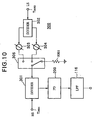
- Figure 10 is a view of an example of the configuration of the three-port MMIC according to the present invention.
- the three-port MMIC 300 comprises, as shown in Fig. 10 , one power detector 200 having, for example, the same structure as Fig. 6 , a received signal RS use input terminal T IN301, a local signal LS use input terminal T IN302, dividers 301 and 302, phase shifters 303 and 304, and a switching circuit 305.
- only one LPF 116 is arranged at a later stage of the three-port MMIC 300.
- the three ports are comprised of the received signal RS use input terminal T IN301 , the local signal LS use input terminal T IN302 , and an output port of the divider 301 to the power detector 200.
- the received signal RS input to the input terminal T IN301 is input to the divider 301.
- the input signal is divided to two signals, and one divided signal is supplied to the power detector 200.
- the local signal input to the input terminal T IN301 is input to the divider 302.
- the input signal is divided to two signals.
- One divided signal is input to the phase shifter 303, shifted in phase by ⁇ , and then supplied to the switching circuit 305.
- the other divided signal is input to the phase shifter 304, shifted in phase by ⁇ , and then supplied to the switching circuit 305.
- the signals shifted in phases by the phase shifters 303 and 304 are selectively supplied to the divider 301 by the switching circuit 305.
- the input signal to the divider 301 is divided to two signals, and one divided signal is supplied to the power detector 200.
- the amplitude component of the supplied signal is detected and the detected amplitude component is supplied to the LPF 116.
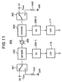
- Figure 11 is a view of an example of the configuration of the four-port MMIC according to the present invention.
- the four-port MMIC 400 comprises, as shown in Fig. 11 , two power detectors 200-1, 200-2 having, for example, the same structures as Fig. 6 , a received signal RS use input terminal T IN401 , a local signal LS use input terminal T IN402 , switching circuits 401 and 402, dividers 403 and 404, and a phase shifter 405.
- two LPF's 116 and 117 are arranged at a later stage of the four-port MMIC 400.
- the four ports are comprised of the received signal RS use input terminal T IN401 , the local signal LS use input terminal T IN402' an output port of the divider 403 to the power detector 200-1, and an output port of the divider 404 to the power detector 200-2.
- the received signal RS input to the input terminal T IN401 is input to the divider 403 through the high-speed switching circuit 401.
- the input signal is divided to two signals. One divided signal is supplied to the power detector 200-1, while the other divided signal is input to the phase shifter 405.
- the received signal from the divider 403 is shifted in phase by ⁇ .
- the signal shifted in phase is input to the divider 404, where the input signal is divided to two signals.
- One divided signal is input to the power detector 200-2, while the other divided signal is supplied to the switching circuit 402.
- the local signal input to the input terminal T IN102 is input to the divider 404 through the high-speed switching circuit 402, and then the local signal is divided to two signals by the divider 404. One divided signal is input to the power detector 200-2, while the other divided signal is input to the phase shifter 405.
- phase shifter 405 the local signal from the divider 404 is shifted in phase by ⁇ .
- the signal shifted in phase is input to the divider 403, where the input signal is divided to two signals.
- One divided signal is input to the power detector 200-1, while the other divided signal is input to the high-speed switching circuit 401.
- the amplitude component of the supplied signal is detected, and the detected amplitude component is supplied to the LPF 116.
- the amplitude component of the supplied signals is detected, and the detected amplitude component is supplied to the LPF 117.
- Figure 12 is a view of an example of the configuration of the six-port MMIC according to the present invention.
- the six-port MMIC 500 comprises, as shown in Fig. 12 , four power detectors 200-1, 200-2, 200-3, and 200-4 having, for example, the same structures as Fig. 6 , a received signal RS use input terminal T IN501 , a local signal LS use input terminal T IN502 , directional couplers 501 and 502, dividers 503 and 504, and a phase shifter 505.
- LPF's 116, 117, 118, and 119 are arranged at a later stage of the six-port MMIC 500.
- the six ports are comprised of the received signal RS use input terminal T IN501 , the local signal LS use input terminal T IN502 , and output port of the directional coupler 501 to the power detector 200-1, an output port of the divider 503 to the power detector 200-2, an output port of the divider 504 to the power detector 200-3, and an output port of the directional coupler 502 to the power detector 200-4.
- the received signal RS input to the input terminal T IN501 is input to the power detector 200-1 and the divider 503 through the directional circuit 501.
- the input signal is divided to two signals. One divided signal is supplied to the power detector 200-2, while the other divided signal is input to the phase shifter 505.
- the received signal from the divider 503 is shifted in phase by ⁇ .
- the signal shifted in phase is input to the divider 504, where the input signal is divided to two signals.
- One divided signal is input to two power detector 200-3, while the other divided signal is supplied to the directional coupler 502.
- the local signal input to the input terminal T IN502 is input to the power detector 200-4 and the divider 504 through the directional coupler 502, and then the local signal is divided to two signals by the divider 504. One divided signal is input to the power detector 200-2, while the other divided signal is input to the phase shifter 505.
- phase shifter 505 the local signal from the divider 504 is shifted in phase by ⁇ .
- the signal shifted in phase is input to the divider 503, where the input signal is divided to two signals.
- One divided signal is input to the power detector 200-2, while the other divided signal is input to the directional coupler 501.
- the power detector 200-1 receives the received signal RS.
- the amplitude component of the supplied signal is detected, and the detected amplitude component is supplied to the LPF 116.
- the power detector 200-2 receives the received signal and the local signal shifted in phase by ⁇ . In the power detector 200-2, amplitude components of the supplied signals are detected, and the detected amplitude components are supplied to the LPF 117.
- the power detector 200-3 receives the local signal and the received signal shifted in phase by ⁇ . In the power detector 200-3, amplitude components of the supplied signals are detected, and the detected amplitude components are supplied to the LPF 118.
- the power detector 200-4 receives the local signal LS. In the power detector 200-4, an amplitude component of the supplied signal is detected, and the detected amplitude component is supplied to the LPF 119.
- the power detector was explained based on the example of Fig. 6 , however, the present invention is not limited to this. Needless to say the present invention can be applied to other types of power detectors.
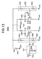
- Figure 13 is a view of another example of the configuration of the power detector according to the present invention.
- the point of difference of the power detector 200A of Fig. 13 from the power detector 200 of Fig. 6 is that the sources of the transistors Q201 and Q202 are directly connected to the ground potential GND in place of connecting through the resistor.
- Figure 14 is a view of another example of the configuration of the power detector according to the present invention.
- the point of difference of the power detector 200B of Fig. 14 from the poser detector 200 of Fig. 6 is that a gate width of W gb of the transistor Q202 is set smaller than a gate width W ga of the transistor Q201, and a resistance Rdb of the drain bias use resistor R207a is larger than a resistance Rda of the drain bias use resistor R206a.
- the ratio W ga /W gb is set to N
- the resistance Rdb of the resistor R207a is set to N times the resistance Rda of the resistor R206a.
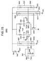
- Figure 15 is a view of another example of the configuration of the power detector according to the present invention.
- connection point of sources of the transistors Q201 and Q202 is connected to the ground potential GND by a field effect transistor Q203 serving as a current source in which a gate is supplied with a bias voltage from a gate bias supplying circuit 204 constituted by resistors R209 and R210 connected in series between the power source V201 and the ground potential GND.
- the universal platform employs the direct conversion approach with the n-port MMIC 115 followed by reconfigurable reprogrammable devices such as DSP's or FPGA's.
- the universal platform is based on the linear operation of the devices.
- the DC offset problem may be solved. It is also possible to support very wide bandwidths compared with conventional I/Q receivers. Therefore, the present universal platform is suitable for multimode and multiband communications.
Landscapes
- Engineering & Computer Science (AREA)
- Computer Networks & Wireless Communication (AREA)
- Signal Processing (AREA)
- Power Engineering (AREA)
- Amplifiers (AREA)
Claims (4)
- Universalplattform für Software-definierte Funkschaltung, aufweisend:einen n-Port-Empfänger (115), n ist eine ganze Zahl von 3 oder mehr, miteinem ersten Eingabeanschluss (Tin101) zum Empfang eines empfangenen Signals (RS),einem zweiten Eingabeanschluss (Tin102) zum Empfang eines lokalen Signals (LS),einer Erzcugungsemrichtung (115), verbunden mit dem ersten und zweiten Eingabeanschluss und aufweisend wenigstens einen Ausgaheanschluss, wobei die Erzeugungseimichtung dient zum Ausgeben an dem wenigstens einen Ausgabeanschluss wenigstens eines Signals, das von dem an dem dann ersten Eingabeanschluss empfangenen Signal abgeleitet ist, und zum selektiven Ausgeben an dem wenigstens einen Ausgabeanschluss von Signalen, die von dem zweiten Eingabeanschluss abgeleitet sind und die eine darauf angewendete Phasenverschiebung (θ) aufweisen,wenigstens einem Leistungsdetektor (1115,1156, 1157) zum Empfang des Ausgabesignals von dem Ausgabeanschluss und Detektieren des Signalpegels des Eingabesignals,wenigstens einem Analog-zu-Digital(A/D)-Umsetzer zum Umsetzen des analogen Ausgabesignals aus dem korrespondierenden Leistungsdetektor in ein digitales Signal undeinem Digitalsignat-Verarbeitimgsteil (102,124 -127,130) zum Umsetzen des Ausgabesignals des Leistungsdetektors durch den A/D-Umsetzsr in mehrere in dem empfangenen Signal oder dem lokalen Signal enthaltene Signalkomponenten,wobei der Digital-Signalverarbeitungsteil wenigstens einen Kompensator (124 - 126) zum Kompensieren der Nicht-Linearität des wenigstens einen Leistungsdetektors aufweist undwobei:der oder jeder Leistungsdetektor aufweiset:einen ersten Feldeffekttransistor (Q201), dessen Gate zum Empfang eines Eingabesignal dient,einen zweiten Feldeffekttransistor (Q202) mit einer mit einer Source, des ersten Feldeffekttransistors verbundenen Source,eine erste Gatevorspannungs-Bercitstellungsschaltung (202) zur Bereitstellung einer Gatevorspannung dem Gate des ersten Feldeffekttransistors,eine zweite Gatevorspannungs-Bereitstellungsschaltung (203) zur Bereitstellung einer Gatevorspannung dem Gate des zweiten Feldeffekdransistors,eine Stromquelle (R205), verbunden mit dem Verbindungspunkt der Sources des ersten Feldeffekttransistors und des zweiten Feldeffekttransistors,eine Drainvorspannungs-Bereitstellungssehaltung zur Bereitstellung einer Drainvorspannung den Drains des ersten Feldeffekttransistors und des zweiten Feldeffekttransistors,einen ersten Kondensator (C202), geschaltet zwischen die Drain des ersten Feldeffekttransistors und ein Referenzpotential, undeinen zweiten Kondensator (C203), geschaltet zwischen die Drain des zweiten Feldeffekttransistors und das Referenzpotential, und wobeidie Spannungsdifferenz zwischen der Drainspannung des ersten Feldeffekttransistors und der Drainspannung des zweiten Feldeffekttransistors als ein Detektions-Ausgabesignal (Vout) verarbeitet wird.
- Universalplattform für Software-definierte Funkschaltung nach Anspruch 1, wobei:der erste Feldeffekttransistor und der zweite Feldeffekttransistor im Wesentlichen äquivalente Charakteristiken aufweisen,die Drainvorspannungs-Bereitstellungsschaltung ein zwischen die Drain des ersten Feldeffekttransistors und eine Spannungsquelle geschaltetes erstes Drainvorspannungseinsatz-Widerstandelement und ein zwischen die Drain des zweiten Feldeffekttransistors und eine Spannungsquelle geschaltetes zweites Drainvorspannungseinsatz-Widerstandselement aufweist,ein Widerstand des ersten Drainvorspamungseinsatz-Widerstandselements und ein Widerstand des zweiten Drainvorspamungseinsatz-Widerstandselements auf im Wesentlichen äquivalente Werte eingestellt sind, undeine Kapazität des ersten Kondensators und eine Kapazität des zweiten Kondensators auf im Wesentlichen äquivalente Werte eingestellt sind.
- Universalplattform für Softwue-definierte Funkschaltung nach Anspruch 1, wobei:wenn eine Gateweite des ersten Feldeffekttransistors Wga ist und eine Gateweite des zweiten Feldeffekttransistors Wgb ist, das Verhältnis Wga/Wgb auf N eingestellt ist,die Drainvorspannungs-Bereitstellungsschaltung ein zwischen die Drain des ersten Feldeffekttransistors und eine Spannungsquelle geschaltetes erstes Drainvorspannungseinsatz-Widerstandselement und ein zwischen die Drain des zweiten Feldeffekttransistors und eine Spannungsquelle geschaltetes zweites Drainvorspannungseinsatz-Widerstandselement aufweist,ein Widerstand Ra des ersten Drainvorspannungseinsatz- Widerstandselements und ein Widerstand Rb des zweiten Drainvorspannungseinsatz-Widerstandselements zum Erfühlen der Bedingung Ra/Rb = 1/N eingestellt sind, undeine Kapazität des ersten Kondensators und eine Kapazität des zweiten Kondensators auf im Wesentlichen äquivalente Werte eingestellt sind.
- Universalplattform für Software-definierte Funkschaltung, aufweisend:einen n-Port-Empfänger (115), n ist eine ganze Zahl von 3 oder mehr, miteinem ersten Eingabeanschluss (Tin101) zum Empfang eines empfangenen Signals (RS),einem zweiten Eingabeanschluss (Tin102) zum Empfang eines lokalen Signals (LS),einer Erzeugungseinrichtung (115), verbunden mit dem ersten und zweiten Eingabeanschluss und aufweisend wenigstens einen Ausgabeanschluss, wobei die Erzeugungseinrichtung dient zum Ausgeben an wenigstens einem Ausgabeanschluss wenigstens eines Signals, das von dem an dem dann ersten Eingabeanschluss empfangenen Signal (RS) abgeleitet ist, und zum selektiven Ausgeben an dem wenigstens einen Ausgabeanschluss von Signalen, die von dem zweiten Eingabeanschluss abgeleitet sind und eine darauf angewendete Phasenverschiebung (θ) aufweisen,wenigstens einem Leistungsdetektor (1135,1156,1157) zum Empfang des Ausgabesignals aus dem Ausgabeanschluss und Detektieren des Signalpegels des Eingabesignals,wenigstens einem Analog-zu-Digital(A/D)-Umsetzer (121,122,123) zum Umsetzen des analogen Ausgabesignals aus dem korrespondierenden Leistimgsdetektor in ein digitales Signal undeinem Digitalsignal-Verarbeitungsteil (102, 124 - 127, 130) zum Umsetzen des Ausgabesignals des Leistungsdetektors durch den A/D-Umsetzar in mehrere in dem empfangenen Signal oder dem lokalen Signal enthaltene Signalkomponenten,wobei der Digitalsignal-Verarbeitungsteil wenigstens einen Kompensator (124-126) zum Kompensieren der Nicht-Lineantät wenigstens des einen Leistungsdetektors aufweist, undwobei;der oder jeder Leistungsdetektor aufweist:einen ersten Feldeffekttransistor (Q201), dessen Gate zum Empfang des Eingabesignals dient und mit einer mit einem Referenzpotential verbundenen Source,einen zweiten Feldeffekttransistor (Q202), mit einer mit dem Referenzpotential verbundenen Source,eine erste Gatevorspamungs-Bereitstellungsschaltung (202) zur Bereitstellung einer Gatevorspannung dem Gate des ersten Feldeffekttransistors,eine zweite Gatevorspannungs-Bereitstellungsschaltung (203) zur Bereitstellung einer Gatevorspannung dem Gate des zweiten Feldeffekttransistors,eine Drainvorspannungs-Bereitstellungsschaltung zur Bereitstellung einer Drainvorspannung den Drains des ersten Feldeffekttransistors und des zweiten Feldeffekttransistors,einen ersten Kondensator (C202), geschaltet zwischen die Drain des ersten Feldeffekttransistors und ein Referenzpotential, undeinen zweiten Kondensator (C203), geschaltet zwischen die Drain des zweiten Feldeffekttransistors und das Referenzpotential, und wobeidie Spannungsdifferenz zwischen der Drainspannung des ersten Feldeffekttransistors und der Drainspannung des zweiten Feldeffekttransistors als ein Detektions-Ausgabesignal (Vout) verarbeitet wird.
Applications Claiming Priority (1)
| Application Number | Priority Date | Filing Date | Title |
|---|---|---|---|
| PCT/JP2000/004550 WO2002005444A1 (en) | 2000-07-07 | 2000-07-07 | Universal platform for software defined radio |
Publications (2)
| Publication Number | Publication Date |
|---|---|
| EP1224742A1 EP1224742A1 (de) | 2002-07-24 |
| EP1224742B1 true EP1224742B1 (de) | 2011-05-18 |
Family
ID=11736239
Family Applications (1)
| Application Number | Title | Priority Date | Filing Date |
|---|---|---|---|
| EP00944337A Expired - Lifetime EP1224742B1 (de) | 2000-07-07 | 2000-07-07 | Universalplattform für softwaredefinierte funkschaltung |
Country Status (5)
| Country | Link |
|---|---|
| US (1) | US6823181B1 (de) |
| EP (1) | EP1224742B1 (de) |
| JP (1) | JP2004503172A (de) |
| AU (1) | AU2000258506A1 (de) |
| WO (1) | WO2002005444A1 (de) |
Families Citing this family (71)
| Publication number | Priority date | Publication date | Assignee | Title |
|---|---|---|---|---|
| US6470055B1 (en) | 1998-08-10 | 2002-10-22 | Kamilo Feher | Spectrally efficient FQPSK, FGMSK, and FQAM for enhanced performance CDMA, TDMA, GSM, OFDN, and other systems |
| US7548787B2 (en) | 2005-08-03 | 2009-06-16 | Kamilo Feher | Medical diagnostic and communication system |
| US7593481B2 (en) | 1998-08-31 | 2009-09-22 | Kamilo Feher | CDMA, W-CDMA, 3rd generation interoperable modem format selectable (MFS) systems with GMSK modulated systems |
| US7079584B2 (en) | 1998-08-10 | 2006-07-18 | Kamilo Feher | OFDM, CDMA, spread spectrum, TDMA, cross-correlated and filtered modulation |
| US6757334B1 (en) * | 1998-08-10 | 2004-06-29 | Kamilo Feher | Bit rate agile third-generation wireless CDMA, GSM, TDMA and OFDM system |
| US7415066B2 (en) | 1998-08-10 | 2008-08-19 | Kamilo Feher | Mis-matched modulation-demodulation format selectable filters |
| US8050345B1 (en) | 1999-08-09 | 2011-11-01 | Kamilo Feher | QAM and GMSK systems |
| US6198777B1 (en) | 1998-08-31 | 2001-03-06 | Kamilo Feher | Feher keying (KF) modualtion and transceivers including clock shaping processors |
| US7015789B1 (en) * | 1999-05-13 | 2006-03-21 | Honeywell International Inc. | State validation using bi-directional wireless link |
| US9373251B2 (en) | 1999-08-09 | 2016-06-21 | Kamilo Feher | Base station devices and automobile wireless communication systems |
| US9813270B2 (en) | 1999-08-09 | 2017-11-07 | Kamilo Feher | Heart rate sensor and medical diagnostics wireless devices |
| US7260369B2 (en) | 2005-08-03 | 2007-08-21 | Kamilo Feher | Location finder, tracker, communication and remote control system |
| US9307407B1 (en) | 1999-08-09 | 2016-04-05 | Kamilo Feher | DNA and fingerprint authentication of mobile devices |
| JP4505981B2 (ja) * | 2000-10-24 | 2010-07-21 | ソニー株式会社 | スペクトル拡散受信機 |
| JP2002291011A (ja) * | 2001-03-23 | 2002-10-04 | Toshiba Corp | 無線装置及び無線装置のハンドオーバ制御方法 |
| KR20030016747A (ko) * | 2001-08-21 | 2003-03-03 | 엘지전자 주식회사 | 이동통신 단말기의 광대역 수신장치 |
| EP1376852B1 (de) * | 2002-06-20 | 2006-11-08 | Sony Deutschland GmbH | I/Q Demodulator unter Verwendung eines Sechs-Tor-Schaltung |
| AU2003263782A1 (en) | 2002-07-12 | 2004-02-02 | Sca Technica, Inc | Self-booting software defined radio module |
| US7885409B2 (en) | 2002-08-28 | 2011-02-08 | Rockwell Collins, Inc. | Software radio system and method |
| US7017140B2 (en) | 2002-08-29 | 2006-03-21 | Bae Systems Information And Electronic Systems Integration Inc. | Common components in interface framework for developing field programmable based applications independent of target circuit board |
| US20040045007A1 (en) | 2002-08-30 | 2004-03-04 | Bae Systems Information Electronic Systems Integration, Inc. | Object oriented component and framework architecture for signal processing |
| DE60224929T2 (de) * | 2002-09-16 | 2009-01-29 | Sony Deutschland Gmbh | Adaptives Selbstkalibrierungsverfahren für einen Quadraturdemodulator eines Fünfport-Empfängers |
| JP2004175052A (ja) * | 2002-11-29 | 2004-06-24 | Sony Corp | インクジェット被記録媒体、インクジェット画像形成方法及び印画物 |
| KR100456961B1 (ko) * | 2002-12-02 | 2004-11-10 | 전자부품연구원 | 에스디알 통신시스템을 위한 베이스밴드 코어 및 그의제어방법 |
| US7386291B2 (en) * | 2003-09-02 | 2008-06-10 | International Business Machines Corporation | Integrated millimeter-wave quadrature generator |
| US7359449B2 (en) | 2004-10-05 | 2008-04-15 | Kamilo Feher | Data communication for wired and wireless communication |
| US8085672B2 (en) * | 2005-01-28 | 2011-12-27 | Honeywell International Inc. | Wireless routing implementation |
| US7826373B2 (en) * | 2005-01-28 | 2010-11-02 | Honeywell International Inc. | Wireless routing systems and methods |
| US7373143B2 (en) * | 2005-02-16 | 2008-05-13 | Par Technology Corporation | Adaptive radio patch interface system |
| US20060223453A1 (en) * | 2005-03-21 | 2006-10-05 | Griffin G S | Frequency shifted wireless local area network system |
| US20060221918A1 (en) * | 2005-04-01 | 2006-10-05 | Hitachi, Ltd. | System, method and computer program product for providing content to a remote device |
| US7848223B2 (en) * | 2005-06-03 | 2010-12-07 | Honeywell International Inc. | Redundantly connected wireless sensor networking methods |
| US7742394B2 (en) * | 2005-06-03 | 2010-06-22 | Honeywell International Inc. | Redundantly connected wireless sensor networking methods |
| US8463319B2 (en) * | 2005-06-17 | 2013-06-11 | Honeywell International Inc. | Wireless application installation, configuration and management tool |
| US7394782B2 (en) * | 2005-07-14 | 2008-07-01 | Honeywell International Inc. | Reduced power time synchronization in wireless communication |
| US7280810B2 (en) | 2005-08-03 | 2007-10-09 | Kamilo Feher | Multimode communication system |
| US10009956B1 (en) | 2017-09-02 | 2018-06-26 | Kamilo Feher | OFDM, 3G and 4G cellular multimode systems and wireless mobile networks |
| US7801094B2 (en) * | 2005-08-08 | 2010-09-21 | Honeywell International Inc. | Integrated infrastructure supporting multiple wireless devices |
| US20070030816A1 (en) * | 2005-08-08 | 2007-02-08 | Honeywell International Inc. | Data compression and abnormal situation detection in a wireless sensor network |
| US7784029B2 (en) * | 2005-09-30 | 2010-08-24 | Microsoft Corporation | Network service for modularly constructing a software defined radio |
| US7681239B2 (en) * | 2005-09-30 | 2010-03-16 | Microsoft Corporation | Modularly constructing a software defined radio |
| US7289466B2 (en) * | 2005-10-05 | 2007-10-30 | Honeywell International Inc. | Localization for low cost sensor network |
| US7603129B2 (en) * | 2005-10-05 | 2009-10-13 | Honeywell International Inc. | Localization identification system for wireless devices |
| US8811231B2 (en) * | 2005-10-21 | 2014-08-19 | Honeywell International Inc. | Wireless transmitter initiated communication systems |
| US8644192B2 (en) * | 2005-10-21 | 2014-02-04 | Honeywell International Inc. | Wireless transmitter initiated communication methods |
| US20070097873A1 (en) * | 2005-10-31 | 2007-05-03 | Honeywell International Inc. | Multiple model estimation in mobile ad-hoc networks |
| US8396041B2 (en) | 2005-11-08 | 2013-03-12 | Microsoft Corporation | Adapting a communication network to varying conditions |
| US8381047B2 (en) | 2005-11-30 | 2013-02-19 | Microsoft Corporation | Predicting degradation of a communication channel below a threshold based on data transmission errors |
| US8285326B2 (en) * | 2005-12-30 | 2012-10-09 | Honeywell International Inc. | Multiprotocol wireless communication backbone |
| US7627060B2 (en) * | 2006-03-21 | 2009-12-01 | Intel Corporation | Receiver and method having envelope compensation signal |
| US7536537B2 (en) * | 2006-04-20 | 2009-05-19 | Harris Corporation | Simultaneous dual booting of platforms |
| US7720506B1 (en) | 2006-07-28 | 2010-05-18 | Rockwell Collins, Inc. | System and method of providing antenna specific front ends for aviation software defined radios |
| US7831255B1 (en) | 2006-07-31 | 2010-11-09 | Rockwell Collins, Inc. | System and method of providing automated availability and integrity verification for aviation software defined radios |
| US7675852B1 (en) | 2006-09-01 | 2010-03-09 | Rockwell Collins, Inc. | System and method of providing bounded dynamic waveform allocation for software defined radios |
| US7847730B2 (en) | 2006-09-27 | 2010-12-07 | Bae Systems Information And Electronic Systems Integration, Inc. | Software defined navigation signal generator |
| US8413227B2 (en) | 2007-09-28 | 2013-04-02 | Honeywell International Inc. | Apparatus and method supporting wireless access to multiple security layers in an industrial control and automation system or other system |
| JP5488459B2 (ja) * | 2008-04-17 | 2014-05-14 | パナソニック株式会社 | 受信装置と、これを用いた電子機器 |
| US20090323784A1 (en) * | 2008-06-27 | 2009-12-31 | Microsoft Corporation | Software-Defined Radio Platform Based Upon Graphics Processing Unit |
| EP2318860A4 (de) | 2008-08-11 | 2012-07-04 | Marport Canada Inc | Phasengesteuertes softwaredefiniertes breitband-multifunktionssonarsystem und verfahren |
| KR100947090B1 (ko) | 2009-05-21 | 2010-03-10 | 엘아이지넥스원 주식회사 | 소프트웨어 정의 무선 무전기의 전력 소모를 감소시키기 위한 방법 |
| US20110105094A1 (en) * | 2009-10-29 | 2011-05-05 | Microsoft Corporation | Location integration in software defined radio |
| US9115908B2 (en) | 2011-07-27 | 2015-08-25 | Honeywell International Inc. | Systems and methods for managing a programmable thermostat |
| US9157764B2 (en) | 2011-07-27 | 2015-10-13 | Honeywell International Inc. | Devices, methods, and systems for occupancy detection |
| US9621371B2 (en) | 2012-07-24 | 2017-04-11 | Honeywell International Inc. | Wireless sensor device with wireless remote programming |
| US8964898B2 (en) * | 2012-09-14 | 2015-02-24 | Northrop Grumman Systems Corporation | Multi-function receiver with switched channelizer having high dynamic range active microwave filters using carbon nanotube electronics |
| US9595987B2 (en) * | 2013-06-12 | 2017-03-14 | Pc-Tel, Inc. | Wide tuning range receiver |
| DE102014221083B4 (de) | 2014-10-16 | 2021-04-01 | Dialog Semiconductor B.V. | Vorrichtung und Verfahren zur Erzeugung einer echten Zufallszahl in Ein-Chip-Systemen (Systems-on-Chip) und Computerprogrammprodukt hierfür |
| CN106603200A (zh) * | 2016-12-12 | 2017-04-26 | 广州慧睿思通信息科技有限公司 | 基于pcie链路的dsp与fpga芯片高速数据传输装置及方法 |
| US10833795B2 (en) | 2018-12-06 | 2020-11-10 | Silicon Laboratories Inc. | System, apparatus and method for optimizing configuration of a wireless transmitter |
| US10833711B2 (en) | 2018-12-19 | 2020-11-10 | Silicon Laboratories Inc. | System, apparatus and method for concurrent reception of multiple channels spaced physically in radio frequency spectrum |
| US11012273B1 (en) | 2019-12-31 | 2021-05-18 | Hughes Network Systems, Llc | Compensating for frequency-dependent I-Q phase imbalance |
Family Cites Families (3)
| Publication number | Priority date | Publication date | Assignee | Title |
|---|---|---|---|---|
| US5079454A (en) | 1990-08-08 | 1992-01-07 | Pacific Monolithics | Temperature compensated FET power detector |
| CA2239681C (en) | 1997-06-10 | 2007-08-21 | Xinping Huang | In-phase and quadrature signal regeneration |
| AU2274899A (en) * | 1997-12-18 | 1999-07-12 | Sony International (Europe) Gmbh | N-port direct receiver |
-
2000
- 2000-07-07 WO PCT/JP2000/004550 patent/WO2002005444A1/en not_active Ceased
- 2000-07-07 AU AU2000258506A patent/AU2000258506A1/en not_active Abandoned
- 2000-07-07 US US10/070,283 patent/US6823181B1/en not_active Expired - Fee Related
- 2000-07-07 EP EP00944337A patent/EP1224742B1/de not_active Expired - Lifetime
- 2000-07-07 JP JP2002509189A patent/JP2004503172A/ja active Pending
Also Published As
| Publication number | Publication date |
|---|---|
| JP2004503172A (ja) | 2004-01-29 |
| US6823181B1 (en) | 2004-11-23 |
| AU2000258506A1 (en) | 2002-01-21 |
| EP1224742A1 (de) | 2002-07-24 |
| WO2002005444A1 (en) | 2002-01-17 |
Similar Documents
| Publication | Publication Date | Title |
|---|---|---|
| US6823181B1 (en) | Universal platform for software defined radio | |
| JP4064473B2 (ja) | nポートダイレクト受信機 | |
| Moghaddasi et al. | Multifunction, multiband, and multimode wireless receivers: A path toward the future | |
| KR100341231B1 (ko) | 이상기 | |
| US10854945B2 (en) | Circuits for wireless communication on multiple frequency bands | |
| US20040002323A1 (en) | Fully integrated self-tuned image rejection downconversion system | |
| Zhang et al. | A power-efficient CMOS multi-band phased-array receiver covering 24–71-GHz utilizing harmonic-selection technique with 36-dB inter-band blocker tolerance for 5G NR | |
| US12149273B2 (en) | System and method for a frequency selective receiver | |
| CN107317588B (zh) | 宽带接收器的设备和方法 | |
| CN104242823A (zh) | 混频开关电路及混频器 | |
| US6356747B1 (en) | Intermediary low-frequency frequency-conversion radiofrequency reception | |
| US6862442B2 (en) | Receiver | |
| US8532238B2 (en) | Subsampling based receiver using frequency selective noise canceller | |
| JP2002135186A (ja) | 受信機 | |
| US20060262230A1 (en) | Receiver if system having image rejection mixer and band-pass filter | |
| EP1330042B1 (de) | Fünfport-topologie für Direktmischung | |
| US20040101067A1 (en) | Demodulator and receiver using it | |
| Kohno et al. | Universal platform for software defined radio | |
| EP0957614A1 (de) | N-Tordemodulator für phasensprung- oder quadraturamplitudenmodulierte Signale | |
| US20050111587A1 (en) | Demodulator and receiver using same | |
| US7123070B2 (en) | High frequency gain amplifier with phase compensation circuit | |
| Wilson et al. | Mixer-first MIMO receiver with multi-port impedance tuning for decoupling of compact antenna systems | |
| US6714602B1 (en) | Demodulator and receiver | |
| EP1296458B1 (de) | Fünf-Tor Empfänger mit passiven Isolation | |
| JP2002271112A (ja) | 信号分配位相切り換え回路及びアクティブアレイアンテナシステム |
Legal Events
| Date | Code | Title | Description |
|---|---|---|---|
| PUAI | Public reference made under article 153(3) epc to a published international application that has entered the european phase |
Free format text: ORIGINAL CODE: 0009012 |
|
| 17P | Request for examination filed |
Effective date: 20020225 |
|
| AK | Designated contracting states |
Kind code of ref document: A1 Designated state(s): AT BE CH CY DE DK ES FI FR GB GR IE IT LI LU MC NL PT SE |
|
| AX | Request for extension of the european patent |
Free format text: AL;LT;LV;MK;RO;SI |
|
| RIN1 | Information on inventor provided before grant (corrected) |
Inventor name: AMIR-ALIKHANI, HAMID,SONY INT. (EUROPE) GMBH Inventor name: VAN ROOYEN, PIETERSONY CORPORATION Inventor name: MICHAEL, LACHLAN B.,SONY COMPUTER SCE. LAB. INC. Inventor name: ABE, MASAYOSHI,SONY CORPORATION Inventor name: SASHO, NOBORU,SONY CORPORATION Inventor name: SWARTS, FRANCISSONY CORPORATION Inventor name: MORELOS-ZARAGOZA, ROBERT, HENRYC/O SONY CORPORATI Inventor name: BRANKOVIC, VESELIN,SONY INT. (EUROPE) GMBH Inventor name: SANADA, YUKITOSHI,SONY COMPUTER SCIENCE LAB. INC. Inventor name: HARUYAMA, SHINICHIROC/O SONY CORPORATION Inventor name: KOHNO, RYUJI,SONY COMPUTER SCIENCE LAB. INC. |
|
| RBV | Designated contracting states (corrected) |
Designated state(s): DE FR GB |
|
| GRAP | Despatch of communication of intention to grant a patent |
Free format text: ORIGINAL CODE: EPIDOSNIGR1 |
|
| RIN1 | Information on inventor provided before grant (corrected) |
Inventor name: KOHNO, RYUJI,SONY COMPUTER SCIENCE LAB. INC. Inventor name: SASHO, NOBORU,SONY CORPORATION Inventor name: ABE, MASAYOSHI,SONY CORPORATION Inventor name: HARUYAMA, SHINICHIROC/O SONY CORPORATION Inventor name: MORELOS-ZARAGOZA, ROBERT, HENRYC/O SONY CORPORATIO Inventor name: SWARTS, FRANCISC/O SONY CORPORATION Inventor name: VAN ROOYEN, PIETERC/O SONY CORPORATION Inventor name: SANADA, YUKITOSHI,SONY COMPUTER SCIENCE LAB. INC. Inventor name: MICHAEL, LACHLAN B.,SONY COMPUTER SCE. LAB. INC. Inventor name: AMIR-ALIKHANI, HAMID,SONY INT. (EUROPE) GMBH Inventor name: BRANKOVIC, VESELIN,SONY INT. (EUROPE) GMBH |
|
| GRAS | Grant fee paid |
Free format text: ORIGINAL CODE: EPIDOSNIGR3 |
|
| GRAA | (expected) grant |
Free format text: ORIGINAL CODE: 0009210 |
|
| AK | Designated contracting states |
Kind code of ref document: B1 Designated state(s): DE FR GB |
|
| REG | Reference to a national code |
Ref country code: GB Ref legal event code: FG4D |
|
| REG | Reference to a national code |
Ref country code: DE Ref legal event code: R096 Ref document number: 60045983 Country of ref document: DE Effective date: 20110630 |
|
| PLBE | No opposition filed within time limit |
Free format text: ORIGINAL CODE: 0009261 |
|
| STAA | Information on the status of an ep patent application or granted ep patent |
Free format text: STATUS: NO OPPOSITION FILED WITHIN TIME LIMIT |
|
| 26N | No opposition filed |
Effective date: 20120221 |
|
| REG | Reference to a national code |
Ref country code: DE Ref legal event code: R097 Ref document number: 60045983 Country of ref document: DE Effective date: 20120221 |
|
| PGFP | Annual fee paid to national office [announced via postgrant information from national office to epo] |
Ref country code: GB Payment date: 20120719 Year of fee payment: 13 |
|
| PGFP | Annual fee paid to national office [announced via postgrant information from national office to epo] |
Ref country code: FR Payment date: 20120806 Year of fee payment: 13 Ref country code: DE Payment date: 20120720 Year of fee payment: 13 |
|
| GBPC | Gb: european patent ceased through non-payment of renewal fee |
Effective date: 20130707 |
|
| REG | Reference to a national code |
Ref country code: FR Ref legal event code: ST Effective date: 20140331 |
|
| PG25 | Lapsed in a contracting state [announced via postgrant information from national office to epo] |
Ref country code: GB Free format text: LAPSE BECAUSE OF NON-PAYMENT OF DUE FEES Effective date: 20130707 Ref country code: DE Free format text: LAPSE BECAUSE OF NON-PAYMENT OF DUE FEES Effective date: 20140201 |
|
| REG | Reference to a national code |
Ref country code: DE Ref legal event code: R119 Ref document number: 60045983 Country of ref document: DE Effective date: 20140201 |
|
| PG25 | Lapsed in a contracting state [announced via postgrant information from national office to epo] |
Ref country code: FR Free format text: LAPSE BECAUSE OF NON-PAYMENT OF DUE FEES Effective date: 20130731 |