EP1225636A2 - Structure et procédé de fabrication d'un transistor MOS avec une resistance de substrat augmentée - Google Patents
Structure et procédé de fabrication d'un transistor MOS avec une resistance de substrat augmentée Download PDFInfo
- Publication number
- EP1225636A2 EP1225636A2 EP20020100045 EP02100045A EP1225636A2 EP 1225636 A2 EP1225636 A2 EP 1225636A2 EP 20020100045 EP20020100045 EP 20020100045 EP 02100045 A EP02100045 A EP 02100045A EP 1225636 A2 EP1225636 A2 EP 1225636A2
- Authority
- EP
- European Patent Office
- Prior art keywords
- transistor
- semiconductor
- doping
- type
- implanting
- Prior art date
- Legal status (The legal status is an assumption and is not a legal conclusion. Google has not performed a legal analysis and makes no representation as to the accuracy of the status listed.)
- Withdrawn
Links
Images


Classifications
-
- H—ELECTRICITY
- H10—SEMICONDUCTOR DEVICES; ELECTRIC SOLID-STATE DEVICES NOT OTHERWISE PROVIDED FOR
- H10P—GENERIC PROCESSES OR APPARATUS FOR THE MANUFACTURE OR TREATMENT OF DEVICES COVERED BY CLASS H10
- H10P30/00—Ion implantation into wafers, substrates or parts of devices
- H10P30/20—Ion implantation into wafers, substrates or parts of devices into semiconductor materials, e.g. for doping
- H10P30/21—Ion implantation into wafers, substrates or parts of devices into semiconductor materials, e.g. for doping of electrically active species
-
- H—ELECTRICITY
- H10—SEMICONDUCTOR DEVICES; ELECTRIC SOLID-STATE DEVICES NOT OTHERWISE PROVIDED FOR
- H10D—INORGANIC ELECTRIC SEMICONDUCTOR DEVICES
- H10D62/00—Semiconductor bodies, or regions thereof, of devices having potential barriers
- H10D62/10—Shapes, relative sizes or dispositions of the regions of the semiconductor bodies; Shapes of the semiconductor bodies
- H10D62/17—Semiconductor regions connected to electrodes not carrying current to be rectified, amplified or switched, e.g. channel regions
- H10D62/351—Substrate regions of field-effect devices
- H10D62/357—Substrate regions of field-effect devices of FETs
- H10D62/364—Substrate regions of field-effect devices of FETs of IGFETs
-
- H—ELECTRICITY
- H10—SEMICONDUCTOR DEVICES; ELECTRIC SOLID-STATE DEVICES NOT OTHERWISE PROVIDED FOR
- H10D—INORGANIC ELECTRIC SEMICONDUCTOR DEVICES
- H10D89/00—Aspects of integrated devices not covered by groups H10D84/00 - H10D88/00
- H10D89/60—Integrated devices comprising arrangements for electrical or thermal protection, e.g. protection circuits against electrostatic discharge [ESD]
- H10D89/601—Integrated devices comprising arrangements for electrical or thermal protection, e.g. protection circuits against electrostatic discharge [ESD] for devices having insulated gate electrodes, e.g. for IGFETs or IGBTs
- H10D89/811—Integrated devices comprising arrangements for electrical or thermal protection, e.g. protection circuits against electrostatic discharge [ESD] for devices having insulated gate electrodes, e.g. for IGFETs or IGBTs using FETs as protective elements
- H10D89/813—Integrated devices comprising arrangements for electrical or thermal protection, e.g. protection circuits against electrostatic discharge [ESD] for devices having insulated gate electrodes, e.g. for IGFETs or IGBTs using FETs as protective elements specially adapted to provide an electrical current path other than the field-effect induced current path
- H10D89/815—Integrated devices comprising arrangements for electrical or thermal protection, e.g. protection circuits against electrostatic discharge [ESD] for devices having insulated gate electrodes, e.g. for IGFETs or IGBTs using FETs as protective elements specially adapted to provide an electrical current path other than the field-effect induced current path involving a parasitic bipolar transistor triggered by the local electrical biasing of the layer acting as base region of said parasitic bipolar transistor
-
- H—ELECTRICITY
- H10—SEMICONDUCTOR DEVICES; ELECTRIC SOLID-STATE DEVICES NOT OTHERWISE PROVIDED FOR
- H10P—GENERIC PROCESSES OR APPARATUS FOR THE MANUFACTURE OR TREATMENT OF DEVICES COVERED BY CLASS H10
- H10P30/00—Ion implantation into wafers, substrates or parts of devices
- H10P30/20—Ion implantation into wafers, substrates or parts of devices into semiconductor materials, e.g. for doping
- H10P30/202—Ion implantation into wafers, substrates or parts of devices into semiconductor materials, e.g. for doping characterised by the semiconductor materials
- H10P30/204—Ion implantation into wafers, substrates or parts of devices into semiconductor materials, e.g. for doping characterised by the semiconductor materials into Group IV semiconductors
-
- H—ELECTRICITY
- H10—SEMICONDUCTOR DEVICES; ELECTRIC SOLID-STATE DEVICES NOT OTHERWISE PROVIDED FOR
- H10P—GENERIC PROCESSES OR APPARATUS FOR THE MANUFACTURE OR TREATMENT OF DEVICES COVERED BY CLASS H10
- H10P30/00—Ion implantation into wafers, substrates or parts of devices
- H10P30/20—Ion implantation into wafers, substrates or parts of devices into semiconductor materials, e.g. for doping
- H10P30/202—Ion implantation into wafers, substrates or parts of devices into semiconductor materials, e.g. for doping characterised by the semiconductor materials
- H10P30/206—Ion implantation into wafers, substrates or parts of devices into semiconductor materials, e.g. for doping characterised by the semiconductor materials into Group III-V semiconductors
-
- H—ELECTRICITY
- H10—SEMICONDUCTOR DEVICES; ELECTRIC SOLID-STATE DEVICES NOT OTHERWISE PROVIDED FOR
- H10P—GENERIC PROCESSES OR APPARATUS FOR THE MANUFACTURE OR TREATMENT OF DEVICES COVERED BY CLASS H10
- H10P30/00—Ion implantation into wafers, substrates or parts of devices
- H10P30/20—Ion implantation into wafers, substrates or parts of devices into semiconductor materials, e.g. for doping
- H10P30/21—Ion implantation into wafers, substrates or parts of devices into semiconductor materials, e.g. for doping of electrically active species
- H10P30/212—Through-implantation
-
- H—ELECTRICITY
- H10—SEMICONDUCTOR DEVICES; ELECTRIC SOLID-STATE DEVICES NOT OTHERWISE PROVIDED FOR
- H10P—GENERIC PROCESSES OR APPARATUS FOR THE MANUFACTURE OR TREATMENT OF DEVICES COVERED BY CLASS H10
- H10P30/00—Ion implantation into wafers, substrates or parts of devices
- H10P30/20—Ion implantation into wafers, substrates or parts of devices into semiconductor materials, e.g. for doping
- H10P30/28—Ion implantation into wafers, substrates or parts of devices into semiconductor materials, e.g. for doping characterised by an annealing step, e.g. for activation of dopants
Definitions
- the present invention is related in general to the field of electronic systems and semiconductor devices, and more specifically to structure and fabrication methods of MOS transistors, which have an increased substrate resistance compared to standard technology.
- Integrated circuits may be severely damaged by electrostatic discharge (ESD) events.
- ESD electrostatic discharge
- a major source of ESD exposure to ICs is from the charged human body ("Human Body Model", HBM); the discharge of the human body generates peak currents of several amperes to the IC for about 100 ns.
- a second source of ESD is from metallic objects ("machine model", MM); it can generate transients with significantly higher rise times than the HBM ESD source.
- a third source is described by the "charged device model” (CDM), in which the IC itself becomes charged and discharges to ground in the opposite direction than the HBM and MM ESD sources. More detail on ESD phenomena and approaches for protection in ICs can be found in A. Amerasekera and C.
- ESD phenomena in ICs are growing in importance as the demand for higher operating speed, smaller operating voltages, higher packing density and reduced cost drives a reduction of all device dimensions. This generally implies thinner dielectric layers, higher doping levels with more abrupt doping transitions, and higher electric fields - all factors that contribute to an increased sensitivity to damaging ESD events.
- MOS metal-oxide-semiconductor
- Second breakdown is a phenomenon that induces thermal runaway in the device wherever the reduction of the impact ionization current is offset by the thermal generation of carriers. Second breakdown is initiated in a device under stress as a result of self-heating. The peak NMOS device temperature, at which second breakdown is initiated, is known to increase with the stress current level.
- One method that is used to improve ESD protection for ICs is biasing the substrate of ESD protection circuits on an IC.
- Such substrate biasing can be effective at improving the response of a multi-finger MOS transistor that is used to conduct an ESD discharge to ground.
- substrate biasing can cause the threshold voltages for devices to change from their nominal values, which may affect device operation.
- substrate biasing under steady-state conditions causes heat generation and increases power losses.
- the challenge of cost reduction implies a drive for minimizing the number of process steps, especially a minimum number of photomask steps, and the application of standardized process conditions wherever possible. These constraints should be kept in mind when additional process steps or new process conditions are proposed to improve ESD insensitivity without sacrificing any desirable device characteristics. An urgent need has, therefore, arisen for a coherent, low-cost method of enhancing ESD insensitivity without the need for additional, real-estate consuming protection devices.
- the device structure should further provide excellent electrical performance, mechanical stability and high reliability.
- the fabrication method should be simple, yet flexible enough for different semiconductor product families and a wide spectrum of design and process variations. Preferably, these innovations should be accomplished without extending production cycle time, and using the installed equipment, so that no investment in new manufacturing machines is needed.
- a structure of a lateral MOS transistor is described, positioned on the surface of an integrated circuit fabricated in a semiconductor of a first conductivity type, comprising a source and a drain, each having at the surface a region of the opposite conductivity type extending to the centrally located gate, defining the active area of said transistor; and a semiconductor region within said semiconductor of the first conductivity type, having a resistivity higher than the remainder of the semiconductor, this region extending vertically below the transistor while laterally limited to the area of the transistor such that the resistivity under the gate is different from the resistivity under the source and drain regions.
- the invention applies to semiconductors both of p-type and n-type as "first" conductivity types; preferably, the semiconductors are in the 1 to 50 ⁇ cm resistivity range.
- the semiconductor may consist of an epitaxial layer deposited on higher conductivity substrate material.
- the region of higher resistivity is the substrate of the transistor, enabling full functioning of the transistor while not affecting operation of neighboring active devices.
- Another aspect of the invention is that the region of higher resistivity improves the ESD protection of the transistor without decreasing latch-up robustness or increasing inadvertent substrate current-induced body biasing of neighboring transistors.
- the method of fabricating the region of higher resistivity under the active area of a high-voltage NMOS transistor having a gate comprises the steps of depositing a photoresist layer over the transistor and opening a window in this layer over the active area of the transistor; then implanting, at high energy, n-doping ions into the p-type semiconductor substrate through the window, creating a deep region having a net p-type doping lower than that of the p-type semiconductor remote from the transistor active area.
- this high-energy ion implant is performed without the need for a new photomask step, since the needed photomask has already been created in a previous ion implant step and is simply re-used.
- This economical feature renders the additional high-energy ion implant step of the present invention exceedingly inexpensive.
- This step can either be performed after a preceding low-energy implant step (needed for defining the extended source and drain of the transistor), or after a preceding medium-energy implant step (needed for defining the deep source and drain of the transistor).
- Another technical advantage of the present invention is the opportunity to implant the high-energy ions so that the peak concentration is at a different depth than that of the p-type semiconductor, and to select the dose so that it overcompensates the p-type semiconductor doping. A region of the opposite conductivity can thus be created, offering a device design for further increasing the p-type substrate resistance.
- the present invention is equally applicable to PMOS transistors; the conductivity types of the semiconductor and the ion implant types are simply reversed.
- FIG. 1 illustrates a commonly used integrated circuit (IC) component 100 in an ESD protection circuit, namely an NMOS transistor which operates in the mode of a lateral bipolar npn transistor during an ESD event and provides a low impedance current path to ground.
- the IC is formed in a semiconductor of a "first conductivity" type; in the example of FIG. 1, this "first conductivity" is p-type, the MOS transistor is an NMOS transistor, and the lateral bipolar transistor is an npn transistor.
- the first conductivity type semiconductor is created by the net doping due to a "substrate” and a "well".
- the term "substrate” refers to the starting semiconductor wafer. In present manufacturing, the substrate typically has p-type doping. For clarity, this case is also selected as the basis for the following discussions. It should be stressed, however, that the invention and all description also cover the case where the substrate has n-type doping.
- the substrate is designated 101. Frequently, but not necessarily, an epitaxial layer 102 of the same conductivity type as the substrate has been deposited over the substrate 101; in this case the term “substrate” refers to epitaxial layer 102 plus starting semiconductor 101.
- a p-well 103 has been formed by localized acceptor ion implantation and annealing.
- n-plus source region 104 (the emitter of the bipolar transistor) and drain region 105 (the collector of the bipolar transistor) were formed by shallow ion implants of donors.
- Layers 107, 108, 109, and 110 provide metallic contacts to the gate, emitter, collector and the wafer backside, respectively.
- FIG. 1 further shows that emitter 108, gate 107 and wafer backside 110 are electrically connected to ground potential.
- a positive voltage spike at the collector applies a reverse bias to the collector/base junction; the base is the substrate 101 (in some devices, epitaxial layer 102 plus the substrate 101); the depletion layer of the space charge region is designated 120.
- the electric field in the depletion region 120 exceeds the breakdown field, avalanching occurs and forms electron/hole pairs. Electrons flow into the collector, and holes flow into the p-type base.
- This hole current I-sub flows from the collector junction through the substrate to the backside contact 110, causing a voltage drop across the resistors R-pwell and R-sub, which positive (forward) biases the emitter/base junction.
- This emitter forward bias is proportional to the effective "substrate resistance" equal to the sum of the resistance components in the current path, which are schematically shown as R-pwell and R-sub in FIG. 1. Those of the electrons injected from the emitter into the base which reach the collector depletion layer will participate in the avalanche mechanism.
- FIG. 2 plots the collector (or drain) current I (on a logarithmic scale) as a function of drain voltage V (on a linear scale). As illustrated in FIG. 2, this snap-back 201 occurs at the collector/drain voltage Vt1 with an associated collector/ drain current It1.
- the field dependence of the avalanche multiplication factor is responsible for establishing a new stable current/voltage equilibrium 202.
- the collector 105 (in FIG. 1) now acts as emitter and diverts the ESD current to the backside substrate contact 110 and to the now reverse biased emitter 104, which now acts as collector.
- the current carrying capability of the device is limited by thermal effects in the avalanching collector depletion layer.
- a number of effects (such as the increase of intrinsic carrier concentration, a reduced carrier mobility, a decrease in thermal conductivity, and a lowering of the potential barrier for tunnel currents) contribute to the onset of the second (thermal) breakdown (203 in FIG. 2).
- the second breakdown trigger current It2 is very sensitive to the device design, especially the doping profiles. Second breakdown results in junction melting and in an irreversible increase in leakage currents. It must, therefore, be avoided for normal device operation.
- FIGs. 3 to 10 The structure of the modified p-well doping and p-well resistance R-pwell according to the present invention are described in FIGs. 3 to 10, and the flexible and economical method for tailoring R-pwell according to the invention is described in FIGs. 11 to 16. While the examples depicted embody the experimental conditions for an NMOS transistor, analogous considerations hold for the conditions of a PMOS transistor.
- FIG. 3 shows in simplified and schematic (not to scale) manner a small portion of an IC having on its surface an MOS transistor, generally designated 300, at a certain stage of its fabrication process according to the invention.
- the invention applies to NMOS as well as PMOS transistors fabricated into semiconductor substrate material.
- the substrate comprises a semiconductor wafer 301 of p-type doping (onto which, for some devices, an epitaxial layer 302, also of p-type doping, has been deposited).
- an epitaxial layer 302 also of p-type doping
- the semiconductor material may be silicon, silicon germanium, gallium arsenide or any other semiconductor material used in IC fabrication.
- the resistivity of the semiconductor substrate, into which the MOS transistor is fabricated ranges from about 1 to 50 ⁇ cm (this is also the resistivity of the epitaxial layer).
- a well 303 of a "first" conductivity type has been fabricated into the substrate.
- this "first" conductivity refers to p-type, for a PMOS transistor, to n-type.
- Silicon dioxide isolation trenches 304 define the active area of the lateral transistor within the p-well.
- the gate 305 of the MOS transistor poly-silicon or another conductive material is usually chosen; its thickness 305a is commonly between 140 and 180 nm, and the width 305b between 0.2 and 1.0 ⁇ m.
- the gate insulator 306 (silicon dioxide, nitrided SiO2, or others) has a physical thickness between 1 and 10 nm.
- FIG. 3 shows a deep source 310 and an extended source 311, further a deep drain 312 and an extended drain 313.
- the extended source and drain are prepared by low- energy, shallow implants (depth typically between 25 and 40 nm), the deep source and drain by medium-energy implants (depth typically between 100 and 140 nm) as part of the process flow shown in FIGs. 11 to 16.
- a window 330a in a photoresist layer 330 is used; window 330a determines the lateral extent and active area of the MOS transistor.
- the same photoresist and window are used for the high-energy implant 340 of the present invention.
- This implant is performed for modifying the well resistivity within the opening of window 330a to an average value at least an order of magnitude higher than the resistivity value of the semiconductor of the first conductivity type.
- the thickness, however, of the photoresist layer 330 is larger than the thickness solely required to block the lower energy implants.
- the photoresist layer thickness is between 1.5 and 2.0 ⁇ m. It the high-energy implant accompanies the medium-energy implant, non-conductive sidewalls 350 are typically present as part of the gate structure. For the options in the process flow, see below.
- the semiconductor well and substrate of the first conductivity type (p-type) (including any epitaxial layer) has dopant species selected from a group consisting of boron, aluminum, gallium, and indium.
- Source, drain, their extensions, and the region of higher resistivity within the semiconductor of the first conductivity type have a dopant species selected from a group consisting of arsenic, phosphorus, antimony, and bismuth.
- the semiconductor well of the first conductivity type has dopant species selected from a group consisting of arsenic, phosphorus, antimony, and bismuth.
- Source, drain, their extensions, and the region of higher resistivity within the semiconductor of the first conductivity type have a dopant species selected from a group consisting of boron, aluminum, gallium, indium, and lithium.
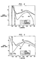
- FIGs. 4 and 5 depict the doping profiles resulting from the high-energy n-doping implant of the present invention, as simulated by computer programs.
- the figures show the profiles of phosphorus implants at 675 keV energy and 2 E13 cm-2 dose into boron-doped silicon substrate material.
- the ordinates in both figures plot the doping concentrations on logarithmic scale, and the abscissa show the penetration depths into the semiconductor surface, expressed in ⁇ m.
- the resulting net doping is illustrated.
- FIG. 4 provides the profiles under the deep source and drain (as illustrated in FIG. 3), and
- FIG. 5 provides the profiles under the poly-silicon gate.
- the counterdoping of the high-energy phosphorus (curve 401) into the original boron doping (curve 402) of the p-type substrate material results in a substantially lowered net doping (curve 403). Consequently, the resulting resistivity is increased.
- the resulting resistivity is in first order uniform between a depth of 0.2 to 0.8 ⁇ m.
- the computer simulation in FIG. 5 indicates that the same phosphorus counterdoping (curve 501) as in FIG. 4 into the original p-type boron doping (curve 502) results in an even lower net doping (still p-type, curve 503) under the gate. There is, of course, no junction under the gate; the gate is heavily doped with phosphorus by an independent process step during formation of the gate.
- FIG. 6 summarizes several counterdoping, high-energy phosphorus ion implants into p-type boron substrate silicon.
- the phosphorus is implanted at the energy of 450 keV.
- Plotted is the measured second breakdown threshold current It2 (expressed in mA/ ⁇ m) as a function of the transistor channel width W (expressed in ⁇ m).
- Diamond data 601 indicate measurements without counterdoping implant.
- the implants are performed at two different doses, with and without annealing after the implant. The most favorable results were obtained by the implant represented by the triangles designated 602. This implant condition has a dose of 8 E12 cm-2, followed by an anneal at 1050 °C for 4 s.
- FIGs. 8, 9, and 10 Another embodiment of the invention is illustrated in FIGs. 8, 9, and 10, again using an NMOS transistor as an example.
- This embodiment illustrates the great versatility of the invention.
- the effective p-type boron doping of the p-well in FIGs. 8 (curve 802) and 9 (curve 902) is the same as the boron doping in FIGs. 4 (curve 402) and 5 (curve 502), respectively.
- the counterdoping phosphorus implant is selected at a somewhat reduced energy (500 keV in FIGs. 8 and 9, versus 675 keV in FIGs. 4 and 5), at the same dose of 2 E13 cm-2. Consequently, the peak penetration is somewhat less deep under the surface.
- FIG. 8 curve 802
- 9 curve 902
- the counterdoping phosphorus implant is selected at a somewhat reduced energy (500 keV in FIGs. 8 and 9, versus 675 keV in FIGs. 4 and 5), at the same dose of 2 E13 cm-2.
- curve 801 the peak phosphorus penetration is in the range of 0.5 to 0.7 ⁇ , as compared to 0.7 to 0.9 ⁇ m for curve 401 in FIG. 4.
- the net doping, though, curve 803, is not substantially different from the net doping achieved in FIG. 4, curve 403.
- the shallower penetration depth of the phosphorus doping peak (curve 901) has a significant effect under the poly-silicon gate.
- the phosphorus doping overcompensates the boron doping (curve 902), leading to a localized slightly n-type region embedded within the p-well.
- This phenomenon is schematically depicted by the NMOS transistor in FIG. 10 (generally designated 1000; not to scale), which is analogous to FIG. 3.
- the phosphorus implant 1040 energy 500 keV and dose 2 E13 cm-2) through the window 1030a of the photoresist layer 1030 into the p-well 1003 results in the volume 1050 having an n-type conductivity opposite to the p-well conductivity.
- Volume 1050 is located vertically under gate 1005 at a depth determined by the implant energy.
- the lateral extent of volume 1050 is approximately equal to the width 1005b of gate 1005.
- the precise boundaries of volume 1050 are determined by the detailed superposition of the doping profiles of the p-well and the compensating ion implant.
- the ESD impact of the appearance of volume 1050 derives from the fact that volume 1050 further impedes the flow of substrate current of transistor 1000.
- the method and process flow for fabricating an IC MOS transistor with increased substrate resistance is outlined in the schematic and simplified FIGs. 11 to 16 for the example of an NMOS transistor; analogous process steps apply for the fabrication of a PMOS transistor.
- the inventive step of implanting the n-doping ions at high energy can be performed either at the step shown in FIG. 13, in sequence with the low-energy implant, or at the step shown in FIG. 16, in sequence with the medium-energy implant.
- the high-energy ion implant is selected at an energy between 400 and 700 keV for a peak concentration at a different depth than that of the p-type semiconductor; dose range about 8 ⁇ 10E12 and 8 ⁇ 10E13 cm-2.
Landscapes
- Metal-Oxide And Bipolar Metal-Oxide Semiconductor Integrated Circuits (AREA)
- Insulated Gate Type Field-Effect Transistor (AREA)
Applications Claiming Priority (2)
| Application Number | Priority Date | Filing Date | Title |
|---|---|---|---|
| US26361901P | 2001-01-23 | 2001-01-23 | |
| US263619 | 2001-01-23 |
Publications (2)
| Publication Number | Publication Date |
|---|---|
| EP1225636A2 true EP1225636A2 (fr) | 2002-07-24 |
| EP1225636A3 EP1225636A3 (fr) | 2006-11-02 |
Family
ID=23002527
Family Applications (1)
| Application Number | Title | Priority Date | Filing Date |
|---|---|---|---|
| EP20020100045 Withdrawn EP1225636A3 (fr) | 2001-01-23 | 2002-01-21 | Structure et procédé de fabrication d'un transistor MOS avec une resistance de substrat augmentée |
Country Status (3)
| Country | Link |
|---|---|
| US (1) | US6627955B2 (fr) |
| EP (1) | EP1225636A3 (fr) |
| JP (1) | JP2002280552A (fr) |
Cited By (1)
| Publication number | Priority date | Publication date | Assignee | Title |
|---|---|---|---|---|
| US20140183708A1 (en) * | 2012-12-28 | 2014-07-03 | United Microelectronics Corporation | Electrostatic discharge protection structure and fabricating method thereof |
Families Citing this family (4)
| Publication number | Priority date | Publication date | Assignee | Title |
|---|---|---|---|---|
| JP2005259953A (ja) | 2004-03-11 | 2005-09-22 | Toshiba Corp | 半導体装置 |
| TW200739876A (en) * | 2005-10-06 | 2007-10-16 | Nxp Bv | Electrostatic discharge protection device |
| JP5839768B2 (ja) | 2008-05-21 | 2016-01-06 | 富士電機株式会社 | 半導体装置の製造方法 |
| US9209098B2 (en) | 2011-05-19 | 2015-12-08 | Taiwan Semiconductor Manufacturing Company, Ltd. | HVMOS reliability evaluation using bulk resistances as indices |
Citations (8)
| Publication number | Priority date | Publication date | Assignee | Title |
|---|---|---|---|---|
| US4701775A (en) | 1985-10-21 | 1987-10-20 | Motorola, Inc. | Buried n- channel implant for NMOS transistors |
| US5359221A (en) | 1992-07-10 | 1994-10-25 | Hitachi, Ltd. | Semiconductor device |
| US5539233A (en) | 1993-07-22 | 1996-07-23 | Texas Instruments Incorporated | Controlled low collector breakdown voltage vertical transistor for ESD protection circuits |
| US5580799A (en) | 1993-11-04 | 1996-12-03 | Victor Company Of Japan, Ltd. | Method of manufacturing transistor with channel implant |
| US5793083A (en) | 1996-11-25 | 1998-08-11 | Texas Instruments Incorporated | Method for designing shallow junction, salicided NMOS transistors with decreased electrostatic discharge sensitivity |
| US5940258A (en) | 1996-02-29 | 1999-08-17 | Texas Instruments Incorporated | Semiconductor ESD protection circuit |
| US5985705A (en) | 1998-06-30 | 1999-11-16 | Lsi Logic Corporation | Low threshold voltage MOS transistor and method of manufacture |
| US6137144A (en) | 1998-04-08 | 2000-10-24 | Texas Instruments Incorporated | On-chip ESD protection in dual voltage CMOS |
Family Cites Families (2)
| Publication number | Priority date | Publication date | Assignee | Title |
|---|---|---|---|---|
| US5923985A (en) * | 1987-01-05 | 1999-07-13 | Seiko Instruments Inc. | MOS field effect transistor and its manufacturing method |
| US6249025B1 (en) * | 1997-12-29 | 2001-06-19 | Intel Corporation | Using epitaxially grown wells for reducing junction capacitances |
-
2002
- 2002-01-14 US US10/043,507 patent/US6627955B2/en not_active Expired - Lifetime
- 2002-01-21 EP EP20020100045 patent/EP1225636A3/fr not_active Withdrawn
- 2002-01-23 JP JP2002014180A patent/JP2002280552A/ja active Pending
Patent Citations (9)
| Publication number | Priority date | Publication date | Assignee | Title |
|---|---|---|---|---|
| US4701775A (en) | 1985-10-21 | 1987-10-20 | Motorola, Inc. | Buried n- channel implant for NMOS transistors |
| US5359221A (en) | 1992-07-10 | 1994-10-25 | Hitachi, Ltd. | Semiconductor device |
| US5539233A (en) | 1993-07-22 | 1996-07-23 | Texas Instruments Incorporated | Controlled low collector breakdown voltage vertical transistor for ESD protection circuits |
| US5580799A (en) | 1993-11-04 | 1996-12-03 | Victor Company Of Japan, Ltd. | Method of manufacturing transistor with channel implant |
| US5940258A (en) | 1996-02-29 | 1999-08-17 | Texas Instruments Incorporated | Semiconductor ESD protection circuit |
| US5793083A (en) | 1996-11-25 | 1998-08-11 | Texas Instruments Incorporated | Method for designing shallow junction, salicided NMOS transistors with decreased electrostatic discharge sensitivity |
| US6137144A (en) | 1998-04-08 | 2000-10-24 | Texas Instruments Incorporated | On-chip ESD protection in dual voltage CMOS |
| US6143594A (en) | 1998-04-08 | 2000-11-07 | Texas Instruments Incorporated | On-chip ESD protection in dual voltage CMOS |
| US5985705A (en) | 1998-06-30 | 1999-11-16 | Lsi Logic Corporation | Low threshold voltage MOS transistor and method of manufacture |
Non-Patent Citations (1)
| Title |
|---|
| K BOCK; C. RUSS; G. BADENES; G. GROESENEKEN; L. DEFERM, PROC. EOS/ESD SYMP., 1997, pages 308 - 315 |
Cited By (3)
| Publication number | Priority date | Publication date | Assignee | Title |
|---|---|---|---|---|
| US20140183708A1 (en) * | 2012-12-28 | 2014-07-03 | United Microelectronics Corporation | Electrostatic discharge protection structure and fabricating method thereof |
| US9378958B2 (en) * | 2012-12-28 | 2016-06-28 | United Microelectronics Corporation | Electrostatic discharge protection structure and fabricating method thereof |
| US9627210B2 (en) | 2012-12-28 | 2017-04-18 | United Microelectronics Corporation | Method of fabricating electrostatic discharge protection structure |
Also Published As
| Publication number | Publication date |
|---|---|
| US20020096716A1 (en) | 2002-07-25 |
| EP1225636A3 (fr) | 2006-11-02 |
| US6627955B2 (en) | 2003-09-30 |
| JP2002280552A (ja) | 2002-09-27 |
Similar Documents
| Publication | Publication Date | Title |
|---|---|---|
| US6822297B2 (en) | Additional n-type LDD/pocket implant for improving short-channel NMOS ESD robustness | |
| US6452236B1 (en) | Channel implant for improving NMOS ESD robustness | |
| US6576959B2 (en) | Device and method of low voltage SCR protection for high voltage failsafe ESD applications | |
| US8891213B2 (en) | Integrated electrostatic discharge (ESD) device | |
| CN100539183C (zh) | 具有附加esd注入的横向双极晶体管 | |
| EP1614156A2 (fr) | Redresseur au silicium basse tension pour protection contre la decharge electrostatique en technologies de silicium sur isolant | |
| US6764892B2 (en) | Device and method of low voltage SCR protection for high voltage failsafe ESD applications | |
| US6767810B2 (en) | Method to increase substrate potential in MOS transistors used in ESD protection circuits | |
| CN108933130B (zh) | 适用于静电放电(esd)保护的半导体装置 | |
| US6724050B2 (en) | ESD improvement by a vertical bipolar transistor with low breakdown voltage and high beta | |
| US7709896B2 (en) | ESD protection device and method | |
| US6433392B1 (en) | Electrostatic discharge device and method | |
| US11508806B1 (en) | Low leakage ESD MOSFET | |
| CN100423256C (zh) | 半导体集成电路中的静电放电保护电路 | |
| US6855609B2 (en) | Method of manufacturing ESD protection structure | |
| US6627955B2 (en) | Structure and method of MOS transistor having increased substrate resistance | |
| US6764909B2 (en) | Structure and method of MOS transistor having increased substrate resistance | |
| KR100698096B1 (ko) | 이에스디(esd) 보호 회로 및 그 제조 방법 | |
| KR100628246B1 (ko) | 이에스디(esd) 보호 회로 및 그 제조 방법 | |
| CN113629052B (zh) | 触发电压可调的esd保护结构及其制备方法 | |
| WO2004008534A2 (fr) | Procede de formation d'un dispositif de protection contre les decharges electrostatiques et agencement de circuit integre comprenant ce dispositif |
Legal Events
| Date | Code | Title | Description |
|---|---|---|---|
| PUAI | Public reference made under article 153(3) epc to a published international application that has entered the european phase |
Free format text: ORIGINAL CODE: 0009012 |
|
| AK | Designated contracting states |
Kind code of ref document: A2 Designated state(s): AT BE CH CY DE DK ES FI FR GB GR IE IT LI LU MC NL PT SE TR |
|
| AX | Request for extension of the european patent |
Free format text: AL;LT;LV;MK;RO;SI |
|
| RIN1 | Information on inventor provided before grant (corrected) |
Inventor name: HU, CHE-JEN Inventor name: WU, ZHIQIANG Inventor name: SALLING, CRAIG T. |
|
| PUAL | Search report despatched |
Free format text: ORIGINAL CODE: 0009013 |
|
| AK | Designated contracting states |
Kind code of ref document: A3 Designated state(s): AT BE CH CY DE DK ES FI FR GB GR IE IT LI LU MC NL PT SE TR |
|
| AX | Request for extension of the european patent |
Extension state: AL LT LV MK RO SI |
|
| 17P | Request for examination filed |
Effective date: 20070502 |
|
| AKX | Designation fees paid |
Designated state(s): AT BE CH CY DE DK ES FI FR GB GR IE IT LI LU MC NL PT SE TR |
|
| 17Q | First examination report despatched |
Effective date: 20070628 |
|
| STAA | Information on the status of an ep patent application or granted ep patent |
Free format text: STATUS: THE APPLICATION IS DEEMED TO BE WITHDRAWN |
|
| 18D | Application deemed to be withdrawn |
Effective date: 20150909 |