EP1227461A2 - Plasma-Anzeigetafel und Verfahren zur Steuerung derselben - Google Patents
Plasma-Anzeigetafel und Verfahren zur Steuerung derselben Download PDFInfo
- Publication number
- EP1227461A2 EP1227461A2 EP01117758A EP01117758A EP1227461A2 EP 1227461 A2 EP1227461 A2 EP 1227461A2 EP 01117758 A EP01117758 A EP 01117758A EP 01117758 A EP01117758 A EP 01117758A EP 1227461 A2 EP1227461 A2 EP 1227461A2
- Authority
- EP
- European Patent Office
- Prior art keywords
- electrodes
- electrode
- discharge
- display panel
- address
- Prior art date
- Legal status (The legal status is an assumption and is not a legal conclusion. Google has not performed a legal analysis and makes no representation as to the accuracy of the status listed.)
- Granted
Links
- 238000000034 method Methods 0.000 title claims description 65
- 238000007599 discharging Methods 0.000 claims description 9
- 230000000977 initiatory effect Effects 0.000 claims description 8
- 238000010586 diagram Methods 0.000 description 34
- 230000002159 abnormal effect Effects 0.000 description 6
- 238000009825 accumulation Methods 0.000 description 3
- 230000007423 decrease Effects 0.000 description 2
- 238000005286 illumination Methods 0.000 description 2
- 150000002500 ions Chemical class 0.000 description 2
- 239000000758 substrate Substances 0.000 description 2
- 230000008859 change Effects 0.000 description 1
- 238000009792 diffusion process Methods 0.000 description 1
- 230000000694 effects Effects 0.000 description 1
- 230000008030 elimination Effects 0.000 description 1
- 238000003379 elimination reaction Methods 0.000 description 1
- 239000011521 glass Substances 0.000 description 1
- 238000004020 luminiscence type Methods 0.000 description 1
- 239000000203 mixture Substances 0.000 description 1
- 230000004048 modification Effects 0.000 description 1
- 238000012986 modification Methods 0.000 description 1
- 230000037452 priming Effects 0.000 description 1
- 230000005855 radiation Effects 0.000 description 1
- 230000009467 reduction Effects 0.000 description 1
Images






Classifications
-
- G—PHYSICS
- G09—EDUCATION; CRYPTOGRAPHY; DISPLAY; ADVERTISING; SEALS
- G09G—ARRANGEMENTS OR CIRCUITS FOR CONTROL OF INDICATING DEVICES USING STATIC MEANS TO PRESENT VARIABLE INFORMATION
- G09G3/00—Control arrangements or circuits, of interest only in connection with visual indicators other than cathode-ray tubes
- G09G3/20—Control arrangements or circuits, of interest only in connection with visual indicators other than cathode-ray tubes for presentation of an assembly of a number of characters, e.g. a page, by composing the assembly by combination of individual elements arranged in a matrix no fixed position being assigned to or needed to be assigned to the individual characters or partial characters
- G09G3/22—Control arrangements or circuits, of interest only in connection with visual indicators other than cathode-ray tubes for presentation of an assembly of a number of characters, e.g. a page, by composing the assembly by combination of individual elements arranged in a matrix no fixed position being assigned to or needed to be assigned to the individual characters or partial characters using controlled light sources
- G09G3/28—Control arrangements or circuits, of interest only in connection with visual indicators other than cathode-ray tubes for presentation of an assembly of a number of characters, e.g. a page, by composing the assembly by combination of individual elements arranged in a matrix no fixed position being assigned to or needed to be assigned to the individual characters or partial characters using controlled light sources using luminous gas-discharge panels, e.g. plasma panels
- G09G3/288—Control arrangements or circuits, of interest only in connection with visual indicators other than cathode-ray tubes for presentation of an assembly of a number of characters, e.g. a page, by composing the assembly by combination of individual elements arranged in a matrix no fixed position being assigned to or needed to be assigned to the individual characters or partial characters using controlled light sources using luminous gas-discharge panels, e.g. plasma panels using AC panels
- G09G3/291—Control arrangements or circuits, of interest only in connection with visual indicators other than cathode-ray tubes for presentation of an assembly of a number of characters, e.g. a page, by composing the assembly by combination of individual elements arranged in a matrix no fixed position being assigned to or needed to be assigned to the individual characters or partial characters using controlled light sources using luminous gas-discharge panels, e.g. plasma panels using AC panels controlling the gas discharge to control a cell condition, e.g. by means of specific pulse shapes
-
- G—PHYSICS
- G09—EDUCATION; CRYPTOGRAPHY; DISPLAY; ADVERTISING; SEALS
- G09G—ARRANGEMENTS OR CIRCUITS FOR CONTROL OF INDICATING DEVICES USING STATIC MEANS TO PRESENT VARIABLE INFORMATION
- G09G3/00—Control arrangements or circuits, of interest only in connection with visual indicators other than cathode-ray tubes
- G09G3/20—Control arrangements or circuits, of interest only in connection with visual indicators other than cathode-ray tubes for presentation of an assembly of a number of characters, e.g. a page, by composing the assembly by combination of individual elements arranged in a matrix no fixed position being assigned to or needed to be assigned to the individual characters or partial characters
- G09G3/22—Control arrangements or circuits, of interest only in connection with visual indicators other than cathode-ray tubes for presentation of an assembly of a number of characters, e.g. a page, by composing the assembly by combination of individual elements arranged in a matrix no fixed position being assigned to or needed to be assigned to the individual characters or partial characters using controlled light sources
- G09G3/28—Control arrangements or circuits, of interest only in connection with visual indicators other than cathode-ray tubes for presentation of an assembly of a number of characters, e.g. a page, by composing the assembly by combination of individual elements arranged in a matrix no fixed position being assigned to or needed to be assigned to the individual characters or partial characters using controlled light sources using luminous gas-discharge panels, e.g. plasma panels
- G09G3/288—Control arrangements or circuits, of interest only in connection with visual indicators other than cathode-ray tubes for presentation of an assembly of a number of characters, e.g. a page, by composing the assembly by combination of individual elements arranged in a matrix no fixed position being assigned to or needed to be assigned to the individual characters or partial characters using controlled light sources using luminous gas-discharge panels, e.g. plasma panels using AC panels
- G09G3/291—Control arrangements or circuits, of interest only in connection with visual indicators other than cathode-ray tubes for presentation of an assembly of a number of characters, e.g. a page, by composing the assembly by combination of individual elements arranged in a matrix no fixed position being assigned to or needed to be assigned to the individual characters or partial characters using controlled light sources using luminous gas-discharge panels, e.g. plasma panels using AC panels controlling the gas discharge to control a cell condition, e.g. by means of specific pulse shapes
- G09G3/292—Control arrangements or circuits, of interest only in connection with visual indicators other than cathode-ray tubes for presentation of an assembly of a number of characters, e.g. a page, by composing the assembly by combination of individual elements arranged in a matrix no fixed position being assigned to or needed to be assigned to the individual characters or partial characters using controlled light sources using luminous gas-discharge panels, e.g. plasma panels using AC panels controlling the gas discharge to control a cell condition, e.g. by means of specific pulse shapes for reset discharge, priming discharge or erase discharge occurring in a phase other than addressing
- G09G3/2927—Details of initialising
-
- G—PHYSICS
- G09—EDUCATION; CRYPTOGRAPHY; DISPLAY; ADVERTISING; SEALS
- G09G—ARRANGEMENTS OR CIRCUITS FOR CONTROL OF INDICATING DEVICES USING STATIC MEANS TO PRESENT VARIABLE INFORMATION
- G09G3/00—Control arrangements or circuits, of interest only in connection with visual indicators other than cathode-ray tubes
- G09G3/20—Control arrangements or circuits, of interest only in connection with visual indicators other than cathode-ray tubes for presentation of an assembly of a number of characters, e.g. a page, by composing the assembly by combination of individual elements arranged in a matrix no fixed position being assigned to or needed to be assigned to the individual characters or partial characters
- G09G3/2007—Display of intermediate tones
- G09G3/2018—Display of intermediate tones by time modulation using two or more time intervals
- G09G3/2022—Display of intermediate tones by time modulation using two or more time intervals using sub-frames
-
- G—PHYSICS
- G09—EDUCATION; CRYPTOGRAPHY; DISPLAY; ADVERTISING; SEALS
- G09G—ARRANGEMENTS OR CIRCUITS FOR CONTROL OF INDICATING DEVICES USING STATIC MEANS TO PRESENT VARIABLE INFORMATION
- G09G3/00—Control arrangements or circuits, of interest only in connection with visual indicators other than cathode-ray tubes
- G09G3/20—Control arrangements or circuits, of interest only in connection with visual indicators other than cathode-ray tubes for presentation of an assembly of a number of characters, e.g. a page, by composing the assembly by combination of individual elements arranged in a matrix no fixed position being assigned to or needed to be assigned to the individual characters or partial characters
- G09G3/22—Control arrangements or circuits, of interest only in connection with visual indicators other than cathode-ray tubes for presentation of an assembly of a number of characters, e.g. a page, by composing the assembly by combination of individual elements arranged in a matrix no fixed position being assigned to or needed to be assigned to the individual characters or partial characters using controlled light sources
- G09G3/28—Control arrangements or circuits, of interest only in connection with visual indicators other than cathode-ray tubes for presentation of an assembly of a number of characters, e.g. a page, by composing the assembly by combination of individual elements arranged in a matrix no fixed position being assigned to or needed to be assigned to the individual characters or partial characters using controlled light sources using luminous gas-discharge panels, e.g. plasma panels
- G09G3/288—Control arrangements or circuits, of interest only in connection with visual indicators other than cathode-ray tubes for presentation of an assembly of a number of characters, e.g. a page, by composing the assembly by combination of individual elements arranged in a matrix no fixed position being assigned to or needed to be assigned to the individual characters or partial characters using controlled light sources using luminous gas-discharge panels, e.g. plasma panels using AC panels
- G09G3/291—Control arrangements or circuits, of interest only in connection with visual indicators other than cathode-ray tubes for presentation of an assembly of a number of characters, e.g. a page, by composing the assembly by combination of individual elements arranged in a matrix no fixed position being assigned to or needed to be assigned to the individual characters or partial characters using controlled light sources using luminous gas-discharge panels, e.g. plasma panels using AC panels controlling the gas discharge to control a cell condition, e.g. by means of specific pulse shapes
- G09G3/292—Control arrangements or circuits, of interest only in connection with visual indicators other than cathode-ray tubes for presentation of an assembly of a number of characters, e.g. a page, by composing the assembly by combination of individual elements arranged in a matrix no fixed position being assigned to or needed to be assigned to the individual characters or partial characters using controlled light sources using luminous gas-discharge panels, e.g. plasma panels using AC panels controlling the gas discharge to control a cell condition, e.g. by means of specific pulse shapes for reset discharge, priming discharge or erase discharge occurring in a phase other than addressing
- G09G3/2922—Details of erasing
-
- G—PHYSICS
- G09—EDUCATION; CRYPTOGRAPHY; DISPLAY; ADVERTISING; SEALS
- G09G—ARRANGEMENTS OR CIRCUITS FOR CONTROL OF INDICATING DEVICES USING STATIC MEANS TO PRESENT VARIABLE INFORMATION
- G09G3/00—Control arrangements or circuits, of interest only in connection with visual indicators other than cathode-ray tubes
- G09G3/20—Control arrangements or circuits, of interest only in connection with visual indicators other than cathode-ray tubes for presentation of an assembly of a number of characters, e.g. a page, by composing the assembly by combination of individual elements arranged in a matrix no fixed position being assigned to or needed to be assigned to the individual characters or partial characters
- G09G3/22—Control arrangements or circuits, of interest only in connection with visual indicators other than cathode-ray tubes for presentation of an assembly of a number of characters, e.g. a page, by composing the assembly by combination of individual elements arranged in a matrix no fixed position being assigned to or needed to be assigned to the individual characters or partial characters using controlled light sources
- G09G3/28—Control arrangements or circuits, of interest only in connection with visual indicators other than cathode-ray tubes for presentation of an assembly of a number of characters, e.g. a page, by composing the assembly by combination of individual elements arranged in a matrix no fixed position being assigned to or needed to be assigned to the individual characters or partial characters using controlled light sources using luminous gas-discharge panels, e.g. plasma panels
- G09G3/288—Control arrangements or circuits, of interest only in connection with visual indicators other than cathode-ray tubes for presentation of an assembly of a number of characters, e.g. a page, by composing the assembly by combination of individual elements arranged in a matrix no fixed position being assigned to or needed to be assigned to the individual characters or partial characters using controlled light sources using luminous gas-discharge panels, e.g. plasma panels using AC panels
- G09G3/291—Control arrangements or circuits, of interest only in connection with visual indicators other than cathode-ray tubes for presentation of an assembly of a number of characters, e.g. a page, by composing the assembly by combination of individual elements arranged in a matrix no fixed position being assigned to or needed to be assigned to the individual characters or partial characters using controlled light sources using luminous gas-discharge panels, e.g. plasma panels using AC panels controlling the gas discharge to control a cell condition, e.g. by means of specific pulse shapes
- G09G3/294—Control arrangements or circuits, of interest only in connection with visual indicators other than cathode-ray tubes for presentation of an assembly of a number of characters, e.g. a page, by composing the assembly by combination of individual elements arranged in a matrix no fixed position being assigned to or needed to be assigned to the individual characters or partial characters using controlled light sources using luminous gas-discharge panels, e.g. plasma panels using AC panels controlling the gas discharge to control a cell condition, e.g. by means of specific pulse shapes for lighting or sustain discharge
-
- G—PHYSICS
- G09—EDUCATION; CRYPTOGRAPHY; DISPLAY; ADVERTISING; SEALS
- G09G—ARRANGEMENTS OR CIRCUITS FOR CONTROL OF INDICATING DEVICES USING STATIC MEANS TO PRESENT VARIABLE INFORMATION
- G09G3/00—Control arrangements or circuits, of interest only in connection with visual indicators other than cathode-ray tubes
- G09G3/20—Control arrangements or circuits, of interest only in connection with visual indicators other than cathode-ray tubes for presentation of an assembly of a number of characters, e.g. a page, by composing the assembly by combination of individual elements arranged in a matrix no fixed position being assigned to or needed to be assigned to the individual characters or partial characters
- G09G3/22—Control arrangements or circuits, of interest only in connection with visual indicators other than cathode-ray tubes for presentation of an assembly of a number of characters, e.g. a page, by composing the assembly by combination of individual elements arranged in a matrix no fixed position being assigned to or needed to be assigned to the individual characters or partial characters using controlled light sources
- G09G3/28—Control arrangements or circuits, of interest only in connection with visual indicators other than cathode-ray tubes for presentation of an assembly of a number of characters, e.g. a page, by composing the assembly by combination of individual elements arranged in a matrix no fixed position being assigned to or needed to be assigned to the individual characters or partial characters using controlled light sources using luminous gas-discharge panels, e.g. plasma panels
- G09G3/288—Control arrangements or circuits, of interest only in connection with visual indicators other than cathode-ray tubes for presentation of an assembly of a number of characters, e.g. a page, by composing the assembly by combination of individual elements arranged in a matrix no fixed position being assigned to or needed to be assigned to the individual characters or partial characters using controlled light sources using luminous gas-discharge panels, e.g. plasma panels using AC panels
- G09G3/296—Driving circuits for producing the waveforms applied to the driving electrodes
-
- G—PHYSICS
- G09—EDUCATION; CRYPTOGRAPHY; DISPLAY; ADVERTISING; SEALS
- G09G—ARRANGEMENTS OR CIRCUITS FOR CONTROL OF INDICATING DEVICES USING STATIC MEANS TO PRESENT VARIABLE INFORMATION
- G09G2310/00—Command of the display device
- G09G2310/06—Details of flat display driving waveforms
- G09G2310/066—Waveforms comprising a gently increasing or decreasing portion, e.g. ramp
-
- G—PHYSICS
- G09—EDUCATION; CRYPTOGRAPHY; DISPLAY; ADVERTISING; SEALS
- G09G—ARRANGEMENTS OR CIRCUITS FOR CONTROL OF INDICATING DEVICES USING STATIC MEANS TO PRESENT VARIABLE INFORMATION
- G09G2320/00—Control of display operating conditions
- G09G2320/02—Improving the quality of display appearance
- G09G2320/0228—Increasing the driving margin in plasma displays
-
- G—PHYSICS
- G09—EDUCATION; CRYPTOGRAPHY; DISPLAY; ADVERTISING; SEALS
- G09G—ARRANGEMENTS OR CIRCUITS FOR CONTROL OF INDICATING DEVICES USING STATIC MEANS TO PRESENT VARIABLE INFORMATION
- G09G3/00—Control arrangements or circuits, of interest only in connection with visual indicators other than cathode-ray tubes
- G09G3/20—Control arrangements or circuits, of interest only in connection with visual indicators other than cathode-ray tubes for presentation of an assembly of a number of characters, e.g. a page, by composing the assembly by combination of individual elements arranged in a matrix no fixed position being assigned to or needed to be assigned to the individual characters or partial characters
- G09G3/22—Control arrangements or circuits, of interest only in connection with visual indicators other than cathode-ray tubes for presentation of an assembly of a number of characters, e.g. a page, by composing the assembly by combination of individual elements arranged in a matrix no fixed position being assigned to or needed to be assigned to the individual characters or partial characters using controlled light sources
- G09G3/28—Control arrangements or circuits, of interest only in connection with visual indicators other than cathode-ray tubes for presentation of an assembly of a number of characters, e.g. a page, by composing the assembly by combination of individual elements arranged in a matrix no fixed position being assigned to or needed to be assigned to the individual characters or partial characters using controlled light sources using luminous gas-discharge panels, e.g. plasma panels
- G09G3/288—Control arrangements or circuits, of interest only in connection with visual indicators other than cathode-ray tubes for presentation of an assembly of a number of characters, e.g. a page, by composing the assembly by combination of individual elements arranged in a matrix no fixed position being assigned to or needed to be assigned to the individual characters or partial characters using controlled light sources using luminous gas-discharge panels, e.g. plasma panels using AC panels
- G09G3/298—Control arrangements or circuits, of interest only in connection with visual indicators other than cathode-ray tubes for presentation of an assembly of a number of characters, e.g. a page, by composing the assembly by combination of individual elements arranged in a matrix no fixed position being assigned to or needed to be assigned to the individual characters or partial characters using controlled light sources using luminous gas-discharge panels, e.g. plasma panels using AC panels using surface discharge panels
- G09G3/299—Control arrangements or circuits, of interest only in connection with visual indicators other than cathode-ray tubes for presentation of an assembly of a number of characters, e.g. a page, by composing the assembly by combination of individual elements arranged in a matrix no fixed position being assigned to or needed to be assigned to the individual characters or partial characters using controlled light sources using luminous gas-discharge panels, e.g. plasma panels using AC panels using surface discharge panels using alternate lighting of surface-type panels
Definitions
- the present invention relates to a plasma display panel and a driving method thereof.
- Aplasma display panel includes two glass substrates having electrodes formed thereon, with a gap of about 100 microns therebetween that is filled with a discharge mixture gas containing Ne, Xe, or the like.
- a voltage that is equal to or greater than the break down voltage (of the discharge gas) is applied between the electrodes to cause a discharge giving a UV radiation, which excites and illuminates phosphors provided on the substrate, thereby displaying an image.
- FIG. 7 is a diagram illustrating a general structure of a plasma display panel device.
- first electrodes (X electrodes) 11 and second electrodes (Y electrodes) 12 are formed so as to be disposed in parallel to each other.
- Third electrodes (address electrodes) 13 are formed so as to cross perpendicularly to the first and second electrodes.
- a first driving circuit 14 supplies a voltage pulse to the first electrodes 11, a second driving circuit 15 supplies a voltage pulse to the second electrodes 12, and a third driving circuit 16 supplies a voltage pulse to the third electrodes 13.
- the first and second electrodes 11 and 12 are provided to initiate a sustain discharge for display illumination .
- the sustain discharge occurs when the voltage pulse is applied repeatedly between the first and second electrodes 11 and 12.
- one of the first and second electrodes 11 and 12 functions as a scan electrode (Y electrode) for writing display data.
- the third electrode 13 is a electrode for selecting a display cell to be illuminated, and applies to a selected cell a voltage for initiating a writing discharge between the third electrode 13 and one of the first electrode 11 and second electrode 12.
- the first, second and third driving circuits 14, 15 and 16 are for generating voltage pulse relative to purposes of the first, second and third electrodes 11, 12 and 13.
- FIG. 8 is a plan view illustrating a display panel portion of the device shown in FIG. 7.
- the X electrode as the first electrode and the Y electrode as the second electrode are disposed parallel to each other.
- electrodes for display lines L1 to L5 are shown.
- the address electrode as the third electrode (A1 to A4) and ribs 2 for dividing discharge cells are formed.
- the panel 10 has the X electrode and the Y electrode as display electrodes alternatively disposed at a constant interval so as to use all gaps between electrodes as display lines (L1, L2).
- Such method is called ALIS method (Alternate Lighting of Surfaces) and disclosed in Japanese Patent No. 2801893. Because all of the gaps between electrodes are used as the display line, a number of electrodes can be a half of that in a plasma display panel having a structure as shown in FIG. 14. Therefore, it is an advantageous method in terms of cost reduction and higher definition.
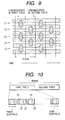
- FIG. 9 is a diagram illustrating a luminescence principle of a plasma display panel using the ALIS method.
- the ALIS method two displaylines share one electrode, and thus, an upper line and a lower line sharing a common electrode cannot be illuminated at the same time. Therefore, similar to an interlaced display in a TV receiver, a display of odd-numbered lines (a first field) and a display of even-numbered lines (a second field) are done alternatively in a time-division manner.
- FIG. 10 is a diagram illustrating a structure of sub-fields in a driving method of a plasma display panel using the ALIS method.
- one frame is composed of a first and a second fields dividing inside thereof .
- each field is divided by a plurality of sub-fields .
- the plasma display panel is either discharged or not-discharged. Therefore, difference in brightness, i.e., gradation, is controlled by a number of discharges.
- the frame includes a plurality of sub-fields each corresponding to a different number of discharges.
- 8 to 12 sub-fields are provided.
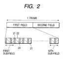
- each sub-field includes a reset period 21, an address period 22, and a sustain discharge period 23 (also called as a sustain period).
- the reset period 21 conducts an operation to reset all the cells in a uniform state, e.g., a state in which wall charge is eliminated, regardless of an illumination state of the previous sub-field.
- the address period 22 selectively discharges (i.e., initiate an address discharge) to form the wall charge to put the cell in ON state.
- the sustain discharge period 23 emits predetermined light by repeating discharges in the cell in which the address discharge has occurred.
- FIGs. 11A to 11E illustrate waveform diagrams of driving waveforms each being applied to each electrode in a plasma display panel employing the ALIS method.
- FIG. 11A shows a pulse supplied to the address electrode;
- FIG. 11B shows a pulse supplied to an X1 electrode;
- FIG. 11C shows a pulse supplied to a Y1 electrode;
- FIG. 11D shows a pulse supplied to an X2 electrode; and
- FIG. 11E shows a pulse supplied to a Y2 electrode.
- a fine pulse -Vy of 1 ⁇ s and about -170V is applied to the Y electrode.
- the ALIS method in odd-numbered fields , lines are illuminated between the X1 -Y1 electrodes , X2 -Y2 electrodes , X3 -Y3 electrodes and so on. In the even-numbered fields, lines are illuminated between Y1-X2 electrodes, Y2-X3 electrodes, Y3-X4 electrodes and so on. Consequently, during the address period, the address pulse is applied to the address electrode, whereas in the address period of the odd-numbered field the scan pulse is applied to Y1, Y2... Yn electrodes. During the address period, in the even-numbered field, the scan pulse is applied to the X2, X3 ...Xn electrodes .
- the sustain pulse is applied to X1-Y1 electrodes, X2-Y2 electrodes, X3-Y3 electrodes, and so on, so that an addressed cell is illuminated.
- the sustain pulse is applied to Y1-X2 electrodes, Y2-X3 electrodes, Y3-X4 electrodes and so on, so that an addressed cell is illuminated.
- FIGs . 12A to 12F show waveform diagrams of voltages applied to a plasma display panel during the sustain discharge period.
- FIG. 12A is a waveform diagram of a voltage applied to the X1 electrode
- FIG. 12B is a waveform diagram of a voltage applied to the Y1 electrode
- FIG. 12C is a waveform diagram of a voltage applied to the X2 electrode
- FIG. 12D is a waveform diagram of a voltage applied to the Y2 electrode
- FIG. 12E is a waveform diagram of a voltage applied to the X3 electrode
- FIG. 12F is a waveform diagram of a voltage applied to the Y3 electrode.
- Black dots represent discharge positions of a discharge by a display line defined by the X2 electrode and the Y2 electrode. In this case, in order to prevent generation of a discharge between the Y1 and X2 electrodes and between the Y2 and X3 electrodes, each electrode is applied with a wide pulse.
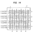
- FIG. 14 is a diagram illustrating a general configuration of other plasma display panel in general. An X electrode and a Y electrode are paired up to form one display line.
- FIGS . 15A to 15C show driving waveforms for driving a plasma display panel shown in FIG. 14, in which, FIG . 15A shows a waveform applied to the address electrode; FIG. 15B shows a waveform applied to the X electrode; and FIG. 15C shows a waveform applied to the Y electrode.
- the driving waveform is based on the disclosure of Japanese Patent No. 2692692 but with a modification to the reset period waveform, and is disclosed in Japanese Translation of Unexamined PCT Application from other countries No. 2000-501199.
- the driving method is characterized in that during the reset period, a wall charge superimposed by an address pulse remains between the address electrode and the Y electrode. Therefore, it is possible to lower voltage of the address pulse and a scan pulse applied during the address period.
- FIGs. 13A to 13D are diagrams illustrating operation of a plasma display panel using the ALIS method as shown in FIGs. 8 to 12F.
- FIG. 13A shows a state in which a sustain discharge is repeatedly initiated between the X2 electrode and the Y2 electrode.
- FIG. 13B electrons generated by the sustain discharge are accumulated as a wall charge as it moves toward adjacent the Y1 electrode or the X3 electrode. Electrons have greater mobility than ions, and thus diffusion toward adjacent cells is easy to occur. On the other hand, ions have less mobility so that accumulation in the adjacent cell does not occur.
- the amount of charge to be stored increases as the interval between electrodes decrease, as the applied voltage increases, and as the number of times sustain discharge is repeated increases.
- the amount of accumulation exceeds certain point, a discharge is initiated between the X1 and Y1 electrodes as shown in FIG. 13C, and thereafter, the sustain discharge occurs repeatedly by the sustain discharge pulse as shown in FIG. 13D.
- an abnormal discharge may occur when the interval between electrodes are narrow, the applied voltages high, and a number of the repetition of the sustain discharge large.
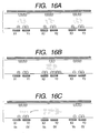
- FIGs. 16A to 16C show diagrams illustrating operation of the plasma display panel as shown in FIGs. 14 and 15A to 15C.
- FIG. 16A shows a state of a wall charge after the reset period and before entering the address period. As previously shown, the wall charge, that is advantageous for an address discharge, remains.
- FIG. 16B shows a state in which the address discharge is initiated in a cell of the X2 electrode and the Y2 electrode.
- FIG. 16C shows a state during the sustain discharge period. It shows that the cell between the X1 electrode and the Y1 electrode starts the discharge because of a priming effect or the like of illuminating cells by repeating the sustain discharges.
- the wall charge formed during the reset period in the present method is advantageous for the address discharge, but may be affect disadvantageously for the sustain discharge period. Particularly, the phenomenon tends to occur in a high definition panel having small intervals between electrodes, and in a case where driving is performed while a large amount of wall charges remain during the reset period.
- An object of the present invention is to solve the above-described problems, and to provide a plasma display panel and a driving method thereof which prevents an abnormal discharge from generating in a cell in which an address discharge is not occurred, the cell adjacent to a cell in which the address discharge is conducted and a sustain discharge is initiated.
- a reset discharge is conducted before an address period to eliminate a wall charge or to make a predetermined amount of wall charge remain therein.
- a discharge is initiated in a cell in which the address discharge does not occur so as to adjust an amount or a polarity of the wall charge.
- the plasma display panel includes a plurality of first electrodes, a plurality of second electrodes disposed alternately and parallel to the first electrode, and a plurality of third electrodes disposed perpendicularly to the first and the second electrodes so as to provide intervals.
- the method includes: a step for resetting; a step for address discharging; a step for sustain discharging; and a charge adjustment step for adjusting a wall charge for a cell having no address discharges occurred therein by applying a voltage for initiating a discharge between the third electrode and one of the first and the second electrodes in the cell having no address discharges occurred therein during either one of a period for the reset step, a period for the address step, and a period for the sustain discharge step.
- a small amount of negative charges are accumulated in a vicinity of the first and the second electrodes in the cell having no address discharges occurred therein.
- the plasma display panel includes a plurality of first electrodes, a plurality of second electrodes disposed alternately and parallel to the first electrode, and a plurality of third electrodes disposed perpendicularly to the first and the second electrodes so as to provide intervals.
- the method includes: a reset step; an address discharge step; and a sustain discharge step; wherein a charge adjustment step is provided for adjusting a wall charge for a cell having no address discharges occurred therein by applying a voltage for initiating a discharge between the third electrode and one of the first and the second electrodes in the cell having no address discharges occurred therein.
- the sustain discharge is occurred one time in a cell in which the address discharge is initiated in the address step, and the charge adjustment step is initiated thereafter.
- the charge adjustment step applies a voltage to initiate a discharge in the cell in which the address discharge does not occur caused by the use of the third electrode as a cathode and either one of the first and the second electrodes as an anode. Moreover, in the charge adjustment step, another one of first and second electrodes has a voltage that does not initiate a discharge between the address electrode and the one of the first and the second electrodes.
- a polarity between the first and the second electrodes is a reversed polarity of a waveform that initiates a discharge between the first and the second electrode at the end of the reset step.
- the charge adjustment step is provided in at least one of a plurality of sub-fields within a field or a frame.
- the charge adjustment step is provided in a sub-field having a large number of times of sustain discharge.
- the charge adjustment step is provided in the first sub-field in the field.
- the voltage for initiating the discharge between the third electrode and the one of the first and second electrodes in the charge adjustment step has a voltage waveform having gentle gradient. Moreover, electrons are formed on both the first and the second electrode in the charge adjustment step.
- the plasma display panel comprises a plurality of first electrodes, a plurality of second electrodes disposed alternately and parallel to the first electrode, and a plurality of third electrodes disposed perpendicularly to the first and the second electrodes so as to provide intervals.
- the method includes: a reset step; an address discharge step; a sustain discharge step; wherein, a charge adjustment step is provided in the reset step so that electrons remain both of the first electrode side and the second electrode side.
- a plasma display panel includes: a plurality of first electrodes, a plurality of second electrodes disposed alternately and parallel to the first electrode, and a plurality of third electrodes disposed perpendicularly to the first and the second electrodes so as to provide intervals.
- a driving circuit is provided to conduct a reset step, an address discharge step, and a charge adjustment step and a sustain discharge step for adjusting a wall charge with respect to a cell, in which the address discharge is not conducted, by applying a voltage which initiates s discharge between the third electrode and one of the first electrode and the second electrode.
- the plasma display panel includes: a plurality of first electrodes, a plurality of second electrodes disposed alternately and parallel to the first electrode, and a plurality of third electrodes disposed perpendicularly to the first and the second electrodes so as to provide intervals.
- a driving circuit is provided for driving a reset and charge adjustment step for making electrons remain in both of the first electrodes and the second electrodes, an address discharge step, and a sustain discharge step.
- FIGs. 1A to 1D show diagrams illustrating a principle of a driving method of a plasma display panel according to the present invention.
- FIG. 1A illustrates a state of a wall charge after a reset period according to a driving waveform as shown in FIGs. 11A to 11E, and a few negative charges remain in X1, X2, and X3 electrodes while a few positive charges remain in Y1, Y2 and Y3 electrodes.
- FIG. 1B illustrates a state of a wall charge after an address discharge occurred in a discharge cell between the X2 electrode and the Y2 electrode. Negative wall charges are accumulated in X2 electrode while positive wall charges are accumulated in Y2 electrode.
- FIG. 1A illustrates a state of a wall charge after a reset period according to a driving waveform as shown in FIGs. 11A to 11E, and a few negative charges remain in X1, X2, and X3 electrodes while a few positive charges remain in Y1, Y2 and
- FIG. 1C illustrates a state in which a sustain discharge is initiated one time after the address discharge. Positive wall charges are accumulated in the X2 electrode while negative wall charges are accumulated in the Y2 electrode. In this state, a few negative wall charges remain in both of the X1 electrode and the X3 electrode , and a few positive wall charges remain in both of the Y1 electrode and the Y3 electrode .
- FIG. 1D illustrates a state in which a discharge is initiated by applying a voltage pulse between the address electrode used as a cathode and the Y electrodes used as an anode, and polarities of wall charges of the Y1 electrodes and Y3 electrode are reversed to be negative wall charges.
- a step illustrated in FIGs. 1C and 1D is provided by the present invention.
- the step is referred as a charge adjustment step, and a period in which the charge adjustment step is performed is referred as a charge adjustment period.
- FIG. 2 illustrates a structure of a sub-field for a purpose of explaining a driving method of a plasma display panel of the present invention.
- the charge adjustment period 24 is provided to adjust an amount of wall charges and a polarity thereof of non-illuminated cell.
- the charge adjustment period 24 may be added to all the sub-fields. Alternatively, it may be added to sub-fields having a large number of times of sustain discharges.
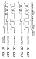
- FIGs. 3A to 3E illustrate waveform diagrams showing a driving method for a plasma display panel according to a first embodiment of the present invention.
- FIG. 3A is a waveform of a voltage applied to the address electrode
- FIG. 3B is a waveform of a voltage applied to the X1 electrode
- FIG. 3C is a waveform of a voltage applied to the Y1 electrode
- FIG. 3D is a waveform of a voltage applied to the X2 electrode
- FIG. 3E is a waveform of a voltage applied to the Y2 electrode. From the reset period to the address period, voltages having waveforms as shown in FIGs. 11A to 11E are applied. It is characterized in that waveforms for charge adjustment are applied after the address period.
- the wall charge of each electrode becomes as is shown in FIG. 1C.
- a discharge for the wall charge adjustment is initiated to a cell in which the address discharge is not initiated and a charge remains.
- the address electrode is in 0V (GND)
- VcX and VcY are applied to the X electrode and the Y electrode, respectively.
- the VcY is a voltage applied between the address electrode and the Y electrode, and its value is set to generate a weak discharge, i.e., 190V.
- the voltage VcX applied to the X electrode is to reduce a potential difference between electrodes so as not to generate any discharge between the address electrode and the Y electrode, and its value is set to 90V. Due to the discharge at the timing of T2, a few negative charges are formed on the Y electrode as shown in FIG. 1D. Therefore, negative charges are accumulated in both X and Y electrodes in the unselected cell, so that any more of electron is prevented from coming or accumulating, thus enabling to prevent a false discharge.
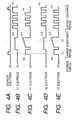
- FIGs. 4A to 4E show waveform diagrams of a driving method of a plasma display panel according to a second embodiment of the present invention, in which, FIG. 4A shows a waveform of a voltage applied to the address electrode during the charge adjustment period and the sustain discharge period; FIG. 4B shows a waveform of a voltage applied to the X1 electrode during the charge adjustment period and the sustain discharge period; FIG. 4C shows a waveform of a voltage applied to the Y1 electrode during the charge adjustment period and the sustain discharge period; FIG. 4D shows a waveform of a voltage applied to the X2 electrode during the charge adjustment period and the sustain discharge period; andFIG. 4E shows a waveform of a voltage applied to the Y2 electrode during the charge adjustment period and the sustain discharge period.
- a voltage waveform VcY having gentle gradient is used as a pulse for the charge adjustment applied at the timing T2 in order to form a few negative charges in the Y electrode.
- the waveform VcY is characterized in that duration of the voltage application is from 50 ⁇ s to 100 ⁇ s. When compared to the previous embodiment, the duration is considerably longer, but no strong discharge would occur at one time because of a gentle gradient in a voltage relative to a change in time. Therefore, even if charge accumulation states are different in each cell, a few negative charges are securely formed on the Y electrode. Values of the voltages VcX and VcY are the same as that in the previous embodiment.
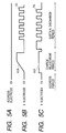
- FIGs. 5A and 5C show waveform diagrams of a driving method of a plasma display panel according to a third embodiment of the present invention in which, FIG. 5A shows a waveform of a voltage applied to the address electrode during the voltage adjustment period and the sustain discharge period; FIG. 5B shows a waveform of a voltage applied to the X electrode during the voltage adjustment period and the sustain discharge period; and FIG. 5C shows a waveform of a voltage applied to the Y electrode during the voltage adjustment period and the sustain discharge period.
- a driving method is applied to a common plasma display panel as shown in FIGs. 14 to 16. From the reset period to the address period, the voltage waveforms are the same as shown in FIGs. 15A to 15C.
- the driving method is characterized in that a wall charge advantageous to the address discharge remains .
- a negative charge is formed on a Y electrode side while a positive charge is formed on an X electrode side.
- the X electrode is applied with a voltage waveform VcX having gentle gradient, and a discharge is initiated between the address electrode and the X electrode, so that the negative charge is formed on the X electrode side.
- the voltage waveform VcX is a voltage of about 200V including a voltage of the wall charge formed by the reset discharge, which initiates a predetermined discharge between the address electrode and the X electrode.
- a voltage waveform VcY applied to the Y electrode is a voltage which prevents a discharge between the X electrode and the Y electrode in a cell in which the address discharge is not initiated. Therefore, the voltage waveform VcY is higher than 0V and lower than the sustain voltage waveform Vs to prevent a discharge in the cell in which the address discharge occurred, i.e., it is about 100V.
- FIGs. 6A to 6E illustrate waveform diagrams of a driving method for a plasma display panel according to a fourth embodiment of the present invention, in which, FIG. 6A is a voltage waveform applied to the address electrode during the reset and charge adjustment period, the address period and the sustain discharge period; FIG. 6B is a voltage waveform applied to the X1 electrode during the reset and charge adjustment period, the address period and the sustain discharge period; FIG. 6C is a voltage waveform applied to the Y1 electrode during the reset and charge adjustment period, the address period and the sustain discharge period; FIG. 6D is a voltage waveform applied to the X2 electrode during the reset and charge adjustment period, the address period and the sustain discharge period; and FIG. 6E is a voltage waveform applied to the Y2 electrode during the reset and charge adjustment period, the address period and the sustain discharge period.
- the present embodiment is characterized in that negative charges are formed in X and Y electrodes in all of cells during the reset period.
- the negative and positive charges are respectively accumulated in the X electrode side and the Y electrode side, by a writing pulse of a voltage waveform Vw having a gentle gradient, the voltage waveform being applied to the Y electrode (Y1, Y2...Yn electrodes).
- the voltage waveform Yx having a gradient as gentle as the voltage waveform Vw is applied to the X electrode (X1, X2, ...Xn electrodes) as the writing pulse.
- the voltage waveform Vx By the voltage waveform Vx, a weak discharge occurred between the X electrode and the address electrode, so that the positive and negative (charges) are formed in the address electrode side and the X electrode side.
- a negative eliminating pulse -Vey having a gentle gradient waveform is applied to the Y electrode, thus eliminating the wall charge. Because both of the Y electrode and the X electrode have negative charges thereon, a voltage Vx applied to the X electrode during an address step is slightly higher than the voltage shown in FIGs. 11A to 11E.
- the present embodiment may be applied to a common plasma display panel and a plasma display panel using the ALIS method.
- the present invention it is possible to prevent an abnormal discharge or a false discharge from occurring in the un-illuminated cell adjacent to the illuminated cell during the sustain discharge period, thus contributing to improve a display quality. It is particularly effective to the ALIS method panel or a plasma display panel using a method in which a charge remains during the reset period.
Landscapes
- Engineering & Computer Science (AREA)
- Physics & Mathematics (AREA)
- Computer Hardware Design (AREA)
- General Physics & Mathematics (AREA)
- Theoretical Computer Science (AREA)
- Power Engineering (AREA)
- Plasma & Fusion (AREA)
- Control Of Indicators Other Than Cathode Ray Tubes (AREA)
- Control Of Gas Discharge Display Tubes (AREA)
Applications Claiming Priority (2)
| Application Number | Priority Date | Filing Date | Title |
|---|---|---|---|
| JP2001009168 | 2001-01-17 | ||
| JP2001009168A JP4422350B2 (ja) | 2001-01-17 | 2001-01-17 | プラズマディスプレイパネルおよびその駆動方法 |
Publications (3)
| Publication Number | Publication Date |
|---|---|
| EP1227461A2 true EP1227461A2 (de) | 2002-07-31 |
| EP1227461A3 EP1227461A3 (de) | 2006-02-01 |
| EP1227461B1 EP1227461B1 (de) | 2010-01-06 |
Family
ID=18876697
Family Applications (1)
| Application Number | Title | Priority Date | Filing Date |
|---|---|---|---|
| EP01117758A Expired - Lifetime EP1227461B1 (de) | 2001-01-17 | 2001-07-31 | Plasma-Anzeige und Verfahren zu ihrer Steuerung |
Country Status (6)
| Country | Link |
|---|---|
| US (1) | US6621229B2 (de) |
| EP (1) | EP1227461B1 (de) |
| JP (1) | JP4422350B2 (de) |
| KR (1) | KR100874311B1 (de) |
| DE (1) | DE60140992D1 (de) |
| TW (1) | TW518536B (de) |
Families Citing this family (19)
| Publication number | Priority date | Publication date | Assignee | Title |
|---|---|---|---|---|
| JP3424587B2 (ja) * | 1998-06-18 | 2003-07-07 | 富士通株式会社 | プラズマディスプレイパネルの駆動方法 |
| KR100675705B1 (ko) | 2001-06-12 | 2007-02-01 | 마츠시타 덴끼 산교 가부시키가이샤 | 플라즈마 디스플레이 장치 |
| JP4675517B2 (ja) * | 2001-07-24 | 2011-04-27 | 株式会社日立製作所 | プラズマディスプレイ装置 |
| KR100607511B1 (ko) * | 2001-08-17 | 2006-08-02 | 엘지전자 주식회사 | 플라즈마 디스플레이 패널의 구동 방법 |
| KR100458569B1 (ko) * | 2002-02-15 | 2004-12-03 | 삼성에스디아이 주식회사 | 플라즈마 디스플레이 패널의 구동방법 |
| JP2004004513A (ja) * | 2002-04-25 | 2004-01-08 | Fujitsu Hitachi Plasma Display Ltd | プラズマディスプレイパネルの駆動方法およびプラズマディスプレイ装置 |
| WO2004051613A1 (ja) * | 2002-11-29 | 2004-06-17 | Matsushita Electric Industrial Co., Ltd. | プラズマディスプレイパネル表示装置およびその駆動方法 |
| EP1471491A3 (de) * | 2003-04-22 | 2005-03-23 | Samsung SDI Co., Ltd. | Plasmabildschirm und Ansteuerverfahren dafür |
| KR100525732B1 (ko) * | 2003-05-23 | 2005-11-04 | 엘지전자 주식회사 | 플라즈마 디스플레이 패널의 구동방법 및 장치 |
| KR100515341B1 (ko) * | 2003-09-02 | 2005-09-15 | 삼성에스디아이 주식회사 | 플라즈마 디스플레이 패널의 구동 장치 |
| JP2005301053A (ja) * | 2004-04-14 | 2005-10-27 | Pioneer Electronic Corp | プラズマディスプレイパネルの駆動方法、駆動回路及び駆動プログラム |
| JP2006267655A (ja) | 2005-03-24 | 2006-10-05 | Fujitsu Hitachi Plasma Display Ltd | プラズマディスプレイパネルの駆動方法およびプラズマディスプレイ装置 |
| KR100705807B1 (ko) * | 2005-06-13 | 2007-04-09 | 엘지전자 주식회사 | 플라즈마 디스플레이 장치 및 그의 구동 방법 |
| JP4987256B2 (ja) * | 2005-06-22 | 2012-07-25 | パナソニック株式会社 | プラズマディスプレイ装置 |
| KR100667551B1 (ko) * | 2005-07-01 | 2007-01-12 | 엘지전자 주식회사 | 플라즈마 디스플레이 패널의 구동장치 및 그 구동방법 |
| KR100890292B1 (ko) * | 2006-02-28 | 2009-03-26 | 파나소닉 주식회사 | 플라즈마 디스플레이 패널의 구동 방법 및 플라즈마디스플레이 장치 |
| JP5007308B2 (ja) * | 2006-11-22 | 2012-08-22 | 株式会社日立製作所 | プラズマディスプレイパネル駆動方法及びプラズマディスプレイ装置 |
| WO2009081448A1 (ja) * | 2007-12-20 | 2009-07-02 | Hitachi, Ltd. | プラズマディスプレイパネルの駆動方法およびプラズマディスプレイ装置 |
| WO2009150851A1 (ja) * | 2008-06-13 | 2009-12-17 | パナソニック株式会社 | プラズマディスプレイ装置およびその駆動方法 |
Citations (4)
| Publication number | Priority date | Publication date | Assignee | Title |
|---|---|---|---|---|
| JP2692692B2 (ja) | 1991-12-20 | 1997-12-17 | 富士通株式会社 | 表示パネルの駆動方法および装置 |
| JP2801893B2 (ja) | 1995-08-03 | 1998-09-21 | 富士通株式会社 | プラズマディスプレイパネル駆動方法及びプラズマディスプレイ装置 |
| EP0959451A2 (de) | 1998-05-20 | 1999-11-24 | Fujitsu Limited | Ansteuerungsverfahren für Plasmaanzeigetafel |
| JP2000501199A (ja) | 1995-11-29 | 2000-02-02 | プラズマコ・インコーポレイテッド | 高コントラストプラズマディスプレイ |
Family Cites Families (1)
| Publication number | Priority date | Publication date | Assignee | Title |
|---|---|---|---|---|
| JP3271598B2 (ja) * | 1999-01-22 | 2002-04-02 | 日本電気株式会社 | Ac型プラズマディスプレイの駆動方法及びac型プラズマディスプレイ |
-
2001
- 2001-01-17 JP JP2001009168A patent/JP4422350B2/ja not_active Expired - Fee Related
- 2001-07-30 KR KR1020010045912A patent/KR100874311B1/ko not_active Expired - Fee Related
- 2001-07-31 DE DE60140992T patent/DE60140992D1/de not_active Expired - Lifetime
- 2001-07-31 TW TW090118628A patent/TW518536B/zh not_active IP Right Cessation
- 2001-07-31 US US09/917,828 patent/US6621229B2/en not_active Expired - Fee Related
- 2001-07-31 EP EP01117758A patent/EP1227461B1/de not_active Expired - Lifetime
Patent Citations (4)
| Publication number | Priority date | Publication date | Assignee | Title |
|---|---|---|---|---|
| JP2692692B2 (ja) | 1991-12-20 | 1997-12-17 | 富士通株式会社 | 表示パネルの駆動方法および装置 |
| JP2801893B2 (ja) | 1995-08-03 | 1998-09-21 | 富士通株式会社 | プラズマディスプレイパネル駆動方法及びプラズマディスプレイ装置 |
| JP2000501199A (ja) | 1995-11-29 | 2000-02-02 | プラズマコ・インコーポレイテッド | 高コントラストプラズマディスプレイ |
| EP0959451A2 (de) | 1998-05-20 | 1999-11-24 | Fujitsu Limited | Ansteuerungsverfahren für Plasmaanzeigetafel |
Also Published As
| Publication number | Publication date |
|---|---|
| US20020093291A1 (en) | 2002-07-18 |
| KR20020062121A (ko) | 2002-07-25 |
| US6621229B2 (en) | 2003-09-16 |
| EP1227461B1 (de) | 2010-01-06 |
| KR100874311B1 (ko) | 2008-12-18 |
| JP4422350B2 (ja) | 2010-02-24 |
| TW518536B (en) | 2003-01-21 |
| EP1227461A3 (de) | 2006-02-01 |
| DE60140992D1 (de) | 2010-02-25 |
| JP2002215085A (ja) | 2002-07-31 |
Similar Documents
| Publication | Publication Date | Title |
|---|---|---|
| US6621229B2 (en) | Plasma display panel and driving method to prevent abnormal discharge | |
| US8094092B2 (en) | Plasma display apparatus and a method of driving the plasma display apparatus | |
| EP0965975B1 (de) | Verfahren und Vorrichtung zur Ansteuerung einer Plasma-Anzeigetafel | |
| EP1047042A2 (de) | Plasmaanzeigegerät mit dessen Steuerungsmethode | |
| EP0929062A2 (de) | Verfahren zur Steuerung einer Plasmaanzeigetafel | |
| JP4251389B2 (ja) | プラズマディスプレイパネルの駆動装置 | |
| US8199072B2 (en) | Plasma display device and method of driving the same | |
| US8294636B2 (en) | Plasma display device and method of driving the same | |
| EP1477959A2 (de) | Plasmaanzeigevorrichtung | |
| JP2000330508A (ja) | プラズマディスプレイパネルの駆動方法 |
Legal Events
| Date | Code | Title | Description |
|---|---|---|---|
| PUAI | Public reference made under article 153(3) epc to a published international application that has entered the european phase |
Free format text: ORIGINAL CODE: 0009012 |
|
| AK | Designated contracting states |
Kind code of ref document: A2 Designated state(s): AT BE CH CY DE DK ES FI FR GB GR IE IT LI LU MC NL PT SE TR |
|
| AX | Request for extension of the european patent |
Free format text: AL;LT;LV;MK;RO;SI |
|
| PUAL | Search report despatched |
Free format text: ORIGINAL CODE: 0009013 |
|
| AK | Designated contracting states |
Kind code of ref document: A3 Designated state(s): AT BE CH CY DE DK ES FI FR GB GR IE IT LI LU MC NL PT SE TR |
|
| AX | Request for extension of the european patent |
Extension state: AL LT LV MK RO SI |
|
| 17P | Request for examination filed |
Effective date: 20060410 |
|
| AKX | Designation fees paid |
Designated state(s): DE FR GB |
|
| 17Q | First examination report despatched |
Effective date: 20061013 |
|
| 17Q | First examination report despatched |
Effective date: 20061013 |
|
| GRAP | Despatch of communication of intention to grant a patent |
Free format text: ORIGINAL CODE: EPIDOSNIGR1 |
|
| GRAS | Grant fee paid |
Free format text: ORIGINAL CODE: EPIDOSNIGR3 |
|
| RIN1 | Information on inventor provided before grant (corrected) |
Inventor name: KANAZAWA, YOSHIKAZUFUJITSU HITACHI PLAS. DIS. LTD Inventor name: HO, SHIRUN,H Inventor name: SUZUKI, KEIZO,H |
|
| RAP1 | Party data changed (applicant data changed or rights of an application transferred) |
Owner name: FUJITSU HITACHI PLASMA DISPLAY LIMITED Owner name: HITACHI, LTD. |
|
| GRAA | (expected) grant |
Free format text: ORIGINAL CODE: 0009210 |
|
| AK | Designated contracting states |
Kind code of ref document: B1 Designated state(s): DE FR GB |
|
| REG | Reference to a national code |
Ref country code: GB Ref legal event code: FG4D |
|
| REF | Corresponds to: |
Ref document number: 60140992 Country of ref document: DE Date of ref document: 20100225 Kind code of ref document: P |
|
| PLBE | No opposition filed within time limit |
Free format text: ORIGINAL CODE: 0009261 |
|
| STAA | Information on the status of an ep patent application or granted ep patent |
Free format text: STATUS: NO OPPOSITION FILED WITHIN TIME LIMIT |
|
| 26N | No opposition filed |
Effective date: 20101007 |
|
| PGFP | Annual fee paid to national office [announced via postgrant information from national office to epo] |
Ref country code: FR Payment date: 20110727 Year of fee payment: 11 |
|
| PGFP | Annual fee paid to national office [announced via postgrant information from national office to epo] |
Ref country code: GB Payment date: 20110727 Year of fee payment: 11 Ref country code: DE Payment date: 20110727 Year of fee payment: 11 |
|
| GBPC | Gb: european patent ceased through non-payment of renewal fee |
Effective date: 20120731 |
|
| REG | Reference to a national code |
Ref country code: FR Ref legal event code: ST Effective date: 20130329 |
|
| PG25 | Lapsed in a contracting state [announced via postgrant information from national office to epo] |
Ref country code: GB Free format text: LAPSE BECAUSE OF NON-PAYMENT OF DUE FEES Effective date: 20120731 Ref country code: FR Free format text: LAPSE BECAUSE OF NON-PAYMENT OF DUE FEES Effective date: 20120731 Ref country code: DE Free format text: LAPSE BECAUSE OF NON-PAYMENT OF DUE FEES Effective date: 20130201 |
|
| REG | Reference to a national code |
Ref country code: DE Ref legal event code: R119 Ref document number: 60140992 Country of ref document: DE Effective date: 20130201 |