EP1227461B1 - Panneau d'affichage à plasma et sa méthode de commande - Google Patents
Panneau d'affichage à plasma et sa méthode de commande Download PDFInfo
- Publication number
- EP1227461B1 EP1227461B1 EP01117758A EP01117758A EP1227461B1 EP 1227461 B1 EP1227461 B1 EP 1227461B1 EP 01117758 A EP01117758 A EP 01117758A EP 01117758 A EP01117758 A EP 01117758A EP 1227461 B1 EP1227461 B1 EP 1227461B1
- Authority
- EP
- European Patent Office
- Prior art keywords
- electrodes
- electrode
- pulse
- discharge
- charge adjustment
- Prior art date
- Legal status (The legal status is an assumption and is not a legal conclusion. Google has not performed a legal analysis and makes no representation as to the accuracy of the status listed.)
- Expired - Lifetime
Links
- 238000000034 method Methods 0.000 title claims description 48
- 230000002459 sustained effect Effects 0.000 claims description 29
- 230000000977 initiatory effect Effects 0.000 claims description 7
- 238000010586 diagram Methods 0.000 description 32
- 230000002159 abnormal effect Effects 0.000 description 5
- 238000009825 accumulation Methods 0.000 description 4
- 230000007423 decrease Effects 0.000 description 2
- 238000005286 illumination Methods 0.000 description 2
- 150000002500 ions Chemical class 0.000 description 2
- 239000000758 substrate Substances 0.000 description 2
- 230000015556 catabolic process Effects 0.000 description 1
- 230000008859 change Effects 0.000 description 1
- 230000001419 dependent effect Effects 0.000 description 1
- 238000009792 diffusion process Methods 0.000 description 1
- 238000007599 discharging Methods 0.000 description 1
- 230000000694 effects Effects 0.000 description 1
- 230000008030 elimination Effects 0.000 description 1
- 238000003379 elimination reaction Methods 0.000 description 1
- 239000011521 glass Substances 0.000 description 1
- 238000004020 luminiscence type Methods 0.000 description 1
- 239000000203 mixture Substances 0.000 description 1
- 230000004048 modification Effects 0.000 description 1
- 238000012986 modification Methods 0.000 description 1
- 230000037452 priming Effects 0.000 description 1
- 230000005855 radiation Effects 0.000 description 1
- 230000009467 reduction Effects 0.000 description 1
Images


Classifications
-
- G—PHYSICS
- G09—EDUCATION; CRYPTOGRAPHY; DISPLAY; ADVERTISING; SEALS
- G09G—ARRANGEMENTS OR CIRCUITS FOR CONTROL OF INDICATING DEVICES USING STATIC MEANS TO PRESENT VARIABLE INFORMATION
- G09G3/00—Control arrangements or circuits, of interest only in connection with visual indicators other than cathode-ray tubes
- G09G3/20—Control arrangements or circuits, of interest only in connection with visual indicators other than cathode-ray tubes for presentation of an assembly of a number of characters, e.g. a page, by composing the assembly by combination of individual elements arranged in a matrix no fixed position being assigned to or needed to be assigned to the individual characters or partial characters
- G09G3/22—Control arrangements or circuits, of interest only in connection with visual indicators other than cathode-ray tubes for presentation of an assembly of a number of characters, e.g. a page, by composing the assembly by combination of individual elements arranged in a matrix no fixed position being assigned to or needed to be assigned to the individual characters or partial characters using controlled light sources
- G09G3/28—Control arrangements or circuits, of interest only in connection with visual indicators other than cathode-ray tubes for presentation of an assembly of a number of characters, e.g. a page, by composing the assembly by combination of individual elements arranged in a matrix no fixed position being assigned to or needed to be assigned to the individual characters or partial characters using controlled light sources using luminous gas-discharge panels, e.g. plasma panels
- G09G3/288—Control arrangements or circuits, of interest only in connection with visual indicators other than cathode-ray tubes for presentation of an assembly of a number of characters, e.g. a page, by composing the assembly by combination of individual elements arranged in a matrix no fixed position being assigned to or needed to be assigned to the individual characters or partial characters using controlled light sources using luminous gas-discharge panels, e.g. plasma panels using AC panels
- G09G3/291—Control arrangements or circuits, of interest only in connection with visual indicators other than cathode-ray tubes for presentation of an assembly of a number of characters, e.g. a page, by composing the assembly by combination of individual elements arranged in a matrix no fixed position being assigned to or needed to be assigned to the individual characters or partial characters using controlled light sources using luminous gas-discharge panels, e.g. plasma panels using AC panels controlling the gas discharge to control a cell condition, e.g. by means of specific pulse shapes
- G09G3/292—Control arrangements or circuits, of interest only in connection with visual indicators other than cathode-ray tubes for presentation of an assembly of a number of characters, e.g. a page, by composing the assembly by combination of individual elements arranged in a matrix no fixed position being assigned to or needed to be assigned to the individual characters or partial characters using controlled light sources using luminous gas-discharge panels, e.g. plasma panels using AC panels controlling the gas discharge to control a cell condition, e.g. by means of specific pulse shapes for reset discharge, priming discharge or erase discharge occurring in a phase other than addressing
- G09G3/2927—Details of initialising
-
- G—PHYSICS
- G09—EDUCATION; CRYPTOGRAPHY; DISPLAY; ADVERTISING; SEALS
- G09G—ARRANGEMENTS OR CIRCUITS FOR CONTROL OF INDICATING DEVICES USING STATIC MEANS TO PRESENT VARIABLE INFORMATION
- G09G3/00—Control arrangements or circuits, of interest only in connection with visual indicators other than cathode-ray tubes
- G09G3/20—Control arrangements or circuits, of interest only in connection with visual indicators other than cathode-ray tubes for presentation of an assembly of a number of characters, e.g. a page, by composing the assembly by combination of individual elements arranged in a matrix no fixed position being assigned to or needed to be assigned to the individual characters or partial characters
- G09G3/2007—Display of intermediate tones
- G09G3/2018—Display of intermediate tones by time modulation using two or more time intervals
- G09G3/2022—Display of intermediate tones by time modulation using two or more time intervals using sub-frames
-
- G—PHYSICS
- G09—EDUCATION; CRYPTOGRAPHY; DISPLAY; ADVERTISING; SEALS
- G09G—ARRANGEMENTS OR CIRCUITS FOR CONTROL OF INDICATING DEVICES USING STATIC MEANS TO PRESENT VARIABLE INFORMATION
- G09G3/00—Control arrangements or circuits, of interest only in connection with visual indicators other than cathode-ray tubes
- G09G3/20—Control arrangements or circuits, of interest only in connection with visual indicators other than cathode-ray tubes for presentation of an assembly of a number of characters, e.g. a page, by composing the assembly by combination of individual elements arranged in a matrix no fixed position being assigned to or needed to be assigned to the individual characters or partial characters
- G09G3/22—Control arrangements or circuits, of interest only in connection with visual indicators other than cathode-ray tubes for presentation of an assembly of a number of characters, e.g. a page, by composing the assembly by combination of individual elements arranged in a matrix no fixed position being assigned to or needed to be assigned to the individual characters or partial characters using controlled light sources
- G09G3/28—Control arrangements or circuits, of interest only in connection with visual indicators other than cathode-ray tubes for presentation of an assembly of a number of characters, e.g. a page, by composing the assembly by combination of individual elements arranged in a matrix no fixed position being assigned to or needed to be assigned to the individual characters or partial characters using controlled light sources using luminous gas-discharge panels, e.g. plasma panels
- G09G3/288—Control arrangements or circuits, of interest only in connection with visual indicators other than cathode-ray tubes for presentation of an assembly of a number of characters, e.g. a page, by composing the assembly by combination of individual elements arranged in a matrix no fixed position being assigned to or needed to be assigned to the individual characters or partial characters using controlled light sources using luminous gas-discharge panels, e.g. plasma panels using AC panels
- G09G3/291—Control arrangements or circuits, of interest only in connection with visual indicators other than cathode-ray tubes for presentation of an assembly of a number of characters, e.g. a page, by composing the assembly by combination of individual elements arranged in a matrix no fixed position being assigned to or needed to be assigned to the individual characters or partial characters using controlled light sources using luminous gas-discharge panels, e.g. plasma panels using AC panels controlling the gas discharge to control a cell condition, e.g. by means of specific pulse shapes
- G09G3/292—Control arrangements or circuits, of interest only in connection with visual indicators other than cathode-ray tubes for presentation of an assembly of a number of characters, e.g. a page, by composing the assembly by combination of individual elements arranged in a matrix no fixed position being assigned to or needed to be assigned to the individual characters or partial characters using controlled light sources using luminous gas-discharge panels, e.g. plasma panels using AC panels controlling the gas discharge to control a cell condition, e.g. by means of specific pulse shapes for reset discharge, priming discharge or erase discharge occurring in a phase other than addressing
- G09G3/2922—Details of erasing
-
- G—PHYSICS
- G09—EDUCATION; CRYPTOGRAPHY; DISPLAY; ADVERTISING; SEALS
- G09G—ARRANGEMENTS OR CIRCUITS FOR CONTROL OF INDICATING DEVICES USING STATIC MEANS TO PRESENT VARIABLE INFORMATION
- G09G3/00—Control arrangements or circuits, of interest only in connection with visual indicators other than cathode-ray tubes
- G09G3/20—Control arrangements or circuits, of interest only in connection with visual indicators other than cathode-ray tubes for presentation of an assembly of a number of characters, e.g. a page, by composing the assembly by combination of individual elements arranged in a matrix no fixed position being assigned to or needed to be assigned to the individual characters or partial characters
- G09G3/22—Control arrangements or circuits, of interest only in connection with visual indicators other than cathode-ray tubes for presentation of an assembly of a number of characters, e.g. a page, by composing the assembly by combination of individual elements arranged in a matrix no fixed position being assigned to or needed to be assigned to the individual characters or partial characters using controlled light sources
- G09G3/28—Control arrangements or circuits, of interest only in connection with visual indicators other than cathode-ray tubes for presentation of an assembly of a number of characters, e.g. a page, by composing the assembly by combination of individual elements arranged in a matrix no fixed position being assigned to or needed to be assigned to the individual characters or partial characters using controlled light sources using luminous gas-discharge panels, e.g. plasma panels
- G09G3/288—Control arrangements or circuits, of interest only in connection with visual indicators other than cathode-ray tubes for presentation of an assembly of a number of characters, e.g. a page, by composing the assembly by combination of individual elements arranged in a matrix no fixed position being assigned to or needed to be assigned to the individual characters or partial characters using controlled light sources using luminous gas-discharge panels, e.g. plasma panels using AC panels
- G09G3/291—Control arrangements or circuits, of interest only in connection with visual indicators other than cathode-ray tubes for presentation of an assembly of a number of characters, e.g. a page, by composing the assembly by combination of individual elements arranged in a matrix no fixed position being assigned to or needed to be assigned to the individual characters or partial characters using controlled light sources using luminous gas-discharge panels, e.g. plasma panels using AC panels controlling the gas discharge to control a cell condition, e.g. by means of specific pulse shapes
- G09G3/294—Control arrangements or circuits, of interest only in connection with visual indicators other than cathode-ray tubes for presentation of an assembly of a number of characters, e.g. a page, by composing the assembly by combination of individual elements arranged in a matrix no fixed position being assigned to or needed to be assigned to the individual characters or partial characters using controlled light sources using luminous gas-discharge panels, e.g. plasma panels using AC panels controlling the gas discharge to control a cell condition, e.g. by means of specific pulse shapes for lighting or sustain discharge
-
- G—PHYSICS
- G09—EDUCATION; CRYPTOGRAPHY; DISPLAY; ADVERTISING; SEALS
- G09G—ARRANGEMENTS OR CIRCUITS FOR CONTROL OF INDICATING DEVICES USING STATIC MEANS TO PRESENT VARIABLE INFORMATION
- G09G3/00—Control arrangements or circuits, of interest only in connection with visual indicators other than cathode-ray tubes
- G09G3/20—Control arrangements or circuits, of interest only in connection with visual indicators other than cathode-ray tubes for presentation of an assembly of a number of characters, e.g. a page, by composing the assembly by combination of individual elements arranged in a matrix no fixed position being assigned to or needed to be assigned to the individual characters or partial characters
- G09G3/22—Control arrangements or circuits, of interest only in connection with visual indicators other than cathode-ray tubes for presentation of an assembly of a number of characters, e.g. a page, by composing the assembly by combination of individual elements arranged in a matrix no fixed position being assigned to or needed to be assigned to the individual characters or partial characters using controlled light sources
- G09G3/28—Control arrangements or circuits, of interest only in connection with visual indicators other than cathode-ray tubes for presentation of an assembly of a number of characters, e.g. a page, by composing the assembly by combination of individual elements arranged in a matrix no fixed position being assigned to or needed to be assigned to the individual characters or partial characters using controlled light sources using luminous gas-discharge panels, e.g. plasma panels
- G09G3/288—Control arrangements or circuits, of interest only in connection with visual indicators other than cathode-ray tubes for presentation of an assembly of a number of characters, e.g. a page, by composing the assembly by combination of individual elements arranged in a matrix no fixed position being assigned to or needed to be assigned to the individual characters or partial characters using controlled light sources using luminous gas-discharge panels, e.g. plasma panels using AC panels
- G09G3/296—Driving circuits for producing the waveforms applied to the driving electrodes
-
- G—PHYSICS
- G09—EDUCATION; CRYPTOGRAPHY; DISPLAY; ADVERTISING; SEALS
- G09G—ARRANGEMENTS OR CIRCUITS FOR CONTROL OF INDICATING DEVICES USING STATIC MEANS TO PRESENT VARIABLE INFORMATION
- G09G2310/00—Command of the display device
- G09G2310/06—Details of flat display driving waveforms
- G09G2310/066—Waveforms comprising a gently increasing or decreasing portion, e.g. ramp
-
- G—PHYSICS
- G09—EDUCATION; CRYPTOGRAPHY; DISPLAY; ADVERTISING; SEALS
- G09G—ARRANGEMENTS OR CIRCUITS FOR CONTROL OF INDICATING DEVICES USING STATIC MEANS TO PRESENT VARIABLE INFORMATION
- G09G2320/00—Control of display operating conditions
- G09G2320/02—Improving the quality of display appearance
- G09G2320/0228—Increasing the driving margin in plasma displays
-
- G—PHYSICS
- G09—EDUCATION; CRYPTOGRAPHY; DISPLAY; ADVERTISING; SEALS
- G09G—ARRANGEMENTS OR CIRCUITS FOR CONTROL OF INDICATING DEVICES USING STATIC MEANS TO PRESENT VARIABLE INFORMATION
- G09G3/00—Control arrangements or circuits, of interest only in connection with visual indicators other than cathode-ray tubes
- G09G3/20—Control arrangements or circuits, of interest only in connection with visual indicators other than cathode-ray tubes for presentation of an assembly of a number of characters, e.g. a page, by composing the assembly by combination of individual elements arranged in a matrix no fixed position being assigned to or needed to be assigned to the individual characters or partial characters
- G09G3/22—Control arrangements or circuits, of interest only in connection with visual indicators other than cathode-ray tubes for presentation of an assembly of a number of characters, e.g. a page, by composing the assembly by combination of individual elements arranged in a matrix no fixed position being assigned to or needed to be assigned to the individual characters or partial characters using controlled light sources
- G09G3/28—Control arrangements or circuits, of interest only in connection with visual indicators other than cathode-ray tubes for presentation of an assembly of a number of characters, e.g. a page, by composing the assembly by combination of individual elements arranged in a matrix no fixed position being assigned to or needed to be assigned to the individual characters or partial characters using controlled light sources using luminous gas-discharge panels, e.g. plasma panels
- G09G3/288—Control arrangements or circuits, of interest only in connection with visual indicators other than cathode-ray tubes for presentation of an assembly of a number of characters, e.g. a page, by composing the assembly by combination of individual elements arranged in a matrix no fixed position being assigned to or needed to be assigned to the individual characters or partial characters using controlled light sources using luminous gas-discharge panels, e.g. plasma panels using AC panels
- G09G3/298—Control arrangements or circuits, of interest only in connection with visual indicators other than cathode-ray tubes for presentation of an assembly of a number of characters, e.g. a page, by composing the assembly by combination of individual elements arranged in a matrix no fixed position being assigned to or needed to be assigned to the individual characters or partial characters using controlled light sources using luminous gas-discharge panels, e.g. plasma panels using AC panels using surface discharge panels
- G09G3/299—Control arrangements or circuits, of interest only in connection with visual indicators other than cathode-ray tubes for presentation of an assembly of a number of characters, e.g. a page, by composing the assembly by combination of individual elements arranged in a matrix no fixed position being assigned to or needed to be assigned to the individual characters or partial characters using controlled light sources using luminous gas-discharge panels, e.g. plasma panels using AC panels using surface discharge panels using alternate lighting of surface-type panels
Definitions
- the present invention relates to a plasma display device having a plasma display panel, and a driving method thereof.
- a plasma display panel includes two glass substrates having electrodes formed thereon, with a gap of about 100 ⁇ m therebetween that is filled with a discharge gas mixture containing Ne, Xe, or the like.
- a voltage that is equal to or greater than the breakdown voltage of the discharge gas is applied between the electrodes to cause a discharge producing UV radiation, which excites and illuminates phosphors provided on the substrate, thereby displaying an image.
- FIG. 1 is a diagram illustrating the general structure of a plasma display device.
- first electrodes 11 On a display panel 10, first electrodes 11 (X electrodes, sustain electrodes) and second electrodes 12 (Y electrodes, scan electrodes) are formed so as to be disposed parallel to each other. Third electrodes 13 (address electrodes) are formed so as to cross orthogonally the first and second electrodes.
- a first driving circuit 14 supplies voltage pulses to the first electrodes 11, a second driving circuit 15 supplies voltage pulses to the second electrodes 12, and a third driving circuit 16 supplies voltage pulses to the third electrodes 13.
- the first and second electrodes 11 and 12 are provided to initiate a sustained discharge for display illumination. The sustained discharge occurs when the voltage pulses are applied repeatedly between the first and second electrodes 11 and 12.
- one of the first and second electrodes 11 and 12 functions as a scan electrode (Y electrode) for writing display data.
- the third electrode 13 is an electrode for selecting a display cell to be illuminated, and applies to a selected cell a voltage for initiating a writing discharge between the third electrode 13 and the first electrode 11 or the second electrode 12.
- the first, second and third driving circuits 14, 15 and 16 are provided for generating voltage pulses to be applied to the first, second and third electrodes 11, 12 and 13, respectively.
- FIG. 2 is a plan view illustrating a display panel portion of the device shown in FIG. 1 .
- the X electrodes as the first electrodes and the Y electrodes as the second electrodes are disposed parallel to each other.
- electrodes for display lines L1 to L5 are shown.
- the display panel portion comprises address electrodes as third electrodes (A1 to A4) and ribs 2 for dividing discharge cells.
- the panel 10 has the X electrodes and the Y electrodes as display electrodes alternatively disposed at constant intervals so as to use all gaps between electrodes as display lines (L1, L2).
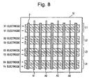
- Such a method is called the ALIS (Alternate Lighting of Surfaces) method; it is disclosed in the patent JP 2801893 . Because all of the gaps between electrodes are used as display lines, the number of electrodes can be half of that in a plasma display panel having a structure as shown in FIG. 8 . Therefore, it is an advantageous method in terms of cost reduction and higher definition.
- FIG. 3 is a diagram illustrating the luminescence principle of a plasma display panel using the ALIS method.
- the ALIS method two display lines share one electrode, and thus, an upper line and a lower line sharing a common electrode cannot be illuminated at the same time. Therefore, similar to an interlaced display in a TV receiver, the display of odd-numbered lines (first field) and the display of even-numbered lines (second field) are done alternatively in a time-division manner.
- FIG. 4 is a diagram illustrating the structure of sub-fields in a driving method of a plasma display panel using the ALIS method.
- one frame is composed of a first field and a second field dividing the frame. Moreover, each field is divided by a plurality of sub-fields.
- the plasma display panel is either discharged or not-discharged. Therefore, the difference in brightness, i,e., the gradation, is controlled by the number of discharges.
- the frame includes a plurality of sub-fields each corresponding to a different number of discharges. Thus, by selectively discharging the sub-field to be illuminated according to the gradation, a different brightness can be achieved. Generally, 8 to 12 sub-fields are provided.
- each sub-field includes a reset period 21, an address period 22 and a sustaining discharge step 23 (also called sustain period).
- the reset period 21 an operation to reset all the cells in a uniform state, e.g., a state in which wall charge is eliminated, regardless of the illumination state of the previous sub-field, is conducted.
- a selective discharge i.e., an address discharge
- the sustaining discharge step 23 predetermined light is emitted by repeating discharges in the cell in which the address discharge has occurred.
- FIGs. 5A to 5E illustrate waveform diagrams of driving waveforms each being applied to each electrode in a plasma display panel employing the ALIS method.
- FIG. 5A shows the pulses supplied to the address electrode;
- FIG. 5B shows the pulses supplied to an X1 electrode;
- FIG. 5C shows the pulses supplied to a Y1 electrode;
- FIG. 5D shows the pulses supplied to an X2 electrode, and
- FIG. 5E shows the pulses supplied to a Y2 electrode.
- a pulse of about -120 V (-Vwx) having a gentle gradient waveform is applied to the X electrode.
- the wall charge is eliminated between the address electrode and the X electrode and between X and Y electrodes of the cell that has been illuminated in the previous sub-field.
- a writing pulse Vw of about 170 V having a gentle gradient waveform is applied to the Y electrode.
- a writing discharge occurs between the Y electrode and the address electrode, and between the Y electrode and the X electrode to form a certain degree of wall charge.
- the ALIS method in odd-numbered fields, lines are illuminated between the X1-Y1 electrodes, X2-Y2 electrodes, X3-Y3 electrodes, and so on. In the even-numbered fields, lines are illuminated between the Y1-X2 electrodes, Y2-X3 electrodes, Y3-X4 electrodes, and so on. Consequently, during the address period, the address pulse is applied to the address electrode, whereas in the address period of the odd-numbered field the scan pulse is applied to the Y1, Y2 ... Yn electrodes. During the address period, in the even-numbered field, the scan pulse is applied to the X2, X3 ...Xn electrodes.
- the sustain pulse is applied to the X1-Y1 electrodes, X2-Y2 electrodes, X3-Y3 electrodes, and so on, so that an addressed cell is illuminated.
- the sustain pulse is applied to Y1-X2 electrodes, Y2-X3 electrodes, Y3-X4 electrodes, and so on, so that an addressed cell is illuminated.
- FIGs. 6A to 6F show waveform diagrams of voltages applied to a plasma display panel during the sustain discharge period.
- FIG. 6A is the waveform diagram of the voltage applied to the X1 electrode
- FIG. 6B is the waveform diagram of the voltage applied to the Y1 electrode
- FIG. 6C is the waveform diagram of the voltage applied to the X2 electrode
- FIG. 6D is the waveform diagram of the voltage applied to the Y2 electrode
- FIG. 6E is the waveform diagram of the voltage applied to the X3 electrode
- FIG. 6F is the waveform diagram of the voltage applied to the Y3 electrode.
- Black dots represent discharge positions of a discharge by a display line defined by the X2 electrode and the Y2 electrode. In this case, in order to prevent generation of a discharge between the Y1 and X2 electrodes and between the Y2 and X3 electrodes, a wide pulse is applied to each electrode.
- FIG. 8 is a diagram illustrating the general configuration of another plasma display panel in general. An X electrode and a Y electrode are paired to form one display line.
- FIGs. 9A to 9C show driving waveforms for driving a plasma display panel as shown in FIG. 8 , in which FIG. 9A shows the waveform applied to the address electrode; FIG. 9B shows the waveform applied to the X electrode, and FIG. 9C shows the waveform applied to the Y electrode.
- the driving waveform is based on the disclosure of the patent JP 2692692 but with a modification to the reset period waveform, and is disclosed in the PCT Application 2000-501199 .
- the driving method is characterized in that during the resent period, a wall charge superimposed by an address pulse remains between the address electrode and the Y electrode. Therefore, it is possible to lower the voltage of the address pulse and a scan pulse applied during the address period.
- FIGs. 7A to 7D are diagrams illustrating the operation of a plasma display panel using the ALIS method as shown in FIGs. 2 to 6F .
- FIG. 7A shows the state in which a sustained discharge is repeatedly initiated between the X2 electrode and the Y2 electrode.
- FIG. 7B electrons generated by the sustained discharge are accumulated as a wall charge as it moves toward the adjacent Y1 electrode or X3 electrode. Electrons have greater mobility than ions, and thus, diffusion toward adjacent cells is easy to occur. On the other hand, ions have less mobility so that an accumulation in the adjacent cell does not occur.
- the amount of charge to be stored increases as the interval between the electrodes decreases, as the applied voltage increases, and as the number of times sustained discharge is repeated increases. When the amount of accumulation exceeds a certain point, a discharge is initiated between the X1 and Y1 electrodes as shown in FIG. 7C , and thereafter, the sustained discharge occurs repeatedly by the sustain discharge pulse as shown in FIG. 7D .
- FIGs. 10A to 10C show diagrams illustrating the operation of the plasma display panel as shown in FIGs. 8 and 9A to 9C .
- FIG. 10A shows the state of a wall charge after the reset period and before entering the address period. As previously shown, the wall charge, that is advantageous for an address discharge, remains.
- FIG. 10B shows the state in which the address discharge is initiated in a cell of the X2 electrode and the Y2 electrode.
- FIG. 10C shows the state during the sustain discharge period. It shows that the cell between the X1 electrode and the Y1 electrode starts the discharge because of a priming effect or the like of illuminating cells by repeating the sustained discharges.
- the wall charge formed during the reset period in the present method is advantageous for the address discharge, but may be affect disadvantageously the sustain discharge period. Particularly, the phenomenon tends to occur in a high definition panel having small intervals between the electrodes, and in the case where driving is performed while a large amount of wall charges remain during the reset period.
- An object of the present invention is to solve the above-described problems and to provide a plasma display device and a driving method thereof which prevents generation of an abnormal discharge in display cells wherein no address discharge occurred during the period between the addressing step and the sustaining discharge step.
- a reset discharge is conducted before an address period to eliminate a wall charge or to make a predetermined amount of wall charge remain therein.
- a discharge is initiated in a cell in which the address discharge does not occur so as to adjust an amount or a polarity of the wall charge.
- the present invention relates to a method for driving plasma display devices which have a plasma display panel 10 which comprises:
- the method is characterized in that for initiating a discharge between the address electrode 13, A1, A2, ... and the sustain electrode 11, X1, X2, ... or the scan electrode 12, Y1, Y2, ... in display cells wherein no address discharge occurred during the period between the addressing step 22 and the sustaining discharge step 23, the charge adjustment step 24 comprises two consecutive stages:
- the present invention further relates to a plasma display device having a plasma display panel 10 which comprises:
- the device of the invention is characterized in that for initiating a discharge between the address electrode 13, A1, A2, ... and the sustain electrode (11, X1, X2, ...) or the scan electrode 12, Y1, Y2, ... in display cells wherein no address discharge occurred during the period between the addressing step 22 and the sustaining discharge step 23, the driving circuits 14, 15, 16 are arranged to conduct the charge adjustment step 24 in such a manner that it comprises two consecutive stages:
- the sustained discharge is occurring one time in a cell in which the address discharge is initiated in the address step, and the charge adjustment step is initiated thereafter.
- the charge adjustment step applies a voltage to initiate a discharge in the cell in which the address discharge does not occur caused by the use of the third electrode as a cathode and either one of the first and the second electrodes as an anode. Moreover, in the charge adjustment step, another one of first and second electrodes has a voltage that does not initiate a discharge between the address electrode and the one of the first and the second electrodes.
- the polarity between the first and the second electrodes is a reversed polarity of the waveform that initiates a discharge between the first and the second electrode at the end of the reset step.
- the charge adjustment step is provided in at least one of a plurality of sub-fields within a field or a frame.
- the charge adjustment step is provided in a sub-field wherein the sustaining discharge step did occur a large number of times.
- the charge adjustment step is provided in the first sub-field within a field or frame.
- the voltage for initiating the discharge between the third electrode and the one of the first and second electrodes in the charge adjustment step has a voltage waveform having a gentle gradient. Moreover, electrons are formed on both the first and the second electrode in the charge adjustment step.
- a charge adjustment step is provided in the reset step so that electrons remain both of the first electrode side and the second electrode side.
- FIGs. 11A to 11D show diagrams illustrating the principle of a driving method of a plasma display panel according to the present invention.
- FIG. 11A illustrates the state of a wall charge after a reset period according to a driving waveform as shown in FIGs. 5A to 5E ; a few negative charges remain at the electrodes X1, X2 and X3 while a few positive charges remain at the electrodes Y1, Y2 and Y3.
- FIG. 11B illustrates the state of the wall charge after an address discharge occurred in a discharge cell between the electrode X2 and the electrode Y2. Negative wall charges are accumulated at the electrode X2 while positive wall charges are accumulated at the electrode Y2.
- FIG. 11A illustrates the state of a wall charge after a reset period according to a driving waveform as shown in FIGs. 5A to 5E ; a few negative charges remain at the electrodes X1, X2 and X3 while a few positive charges remain at the electrodes Y1, Y2 and
- FIG. 11C illustrates the state in which a sustained discharge is initiated one time after the address discharge by a pulse Vw being applied, the pulse Vw having a voltage equal to that of the sustained pulse.
- Positive wall charges are accumulated at electrode X2 while negative wall charges are accumulated at electrode Y2.
- FIG. 11D illustrates the state in which a discharge is initiated by applying a voltage pulse between the address electrode used as a cathode and the Y electrodes used as an anode, and the polarities of the wall charges of the electrodes Y1 and Y3 are reversed to be negative wall charges.
- the step illustrated in FIGs. 11C and 11D is provided by the present invention.
- the step is referred to as a charge adjustment step, and the period in which the charge adjustment step is performed is referred to as a charge adjustment period.
- FIG. 12 illustrates the structure of a sub-field for the purpose of explaining the driving method of the present invention.
- the charge adjustment step 24 is provided to adjust the amount of wall charges and the polarity thereof of a non-illuminated cell.
- the charge adjustment step 24 may be added to all the sub-fields. Alternatively, it may be added to sub-fields wherein the sustaining discharge step 23 did occur a large number of times.
- FIGs. 13A to 13E illustrate waveform diagrams showing the driving method for a plasma display panel according to a first embodiment of the present invention.
- FIG. 13A is the waveform of the voltage applied to the address electrode;
- FIG. 13B is the waveform of the voltage applied to the X1 electrode;
- FIG. 13C is the waveform of the voltage applied to the Y1 electrode;
- FIG. 13D is the waveform of the voltage applied to the X2 electrode, and
- FIG. 13E is the waveform of the voltage applied to the Y2 electrode. From the reset period to the addressing period, voltages having waveforms as shown in FIGs. 5A to 5E are applied. It is characteristic that the waveforms for charge adjustment are applied after the addressing period.
- the wall charge of each electrode becomes as is shown in FIG. 11C .
- a discharge for the wall charge adjustment is initiated at a cell in which the address discharge is not initiated and a charge remains.
- the address electrode is at 0 V (GND)
- pulses VcX and VcY are applied to the X electrode and the Y electrode, respectively.
- VcY is the voltage applied between the address electrode and the Y electrode., and its value is set to generate a weak discharge, i.e., 190 V.
- the voltage VcX applied to the X electrode is to reduce a potential difference between electrodes so as not to generate any discharge between the address electrode and the Y electrode, and its value is set to 90 V. Due to the discharge at the time of T2, a few negative charges are formed on the Y electrode as shown in FIG. 11D . Therefore, negative charges are accumulated in both X and Y electrodes in the unselected cell, so that any higher accumulation of electrons is prevented, and thus, false discharges can be prevented.
- FIGs. 14A to 14E show waveform diagrams of the driving method of a plasma display panel according to a second embodiment of the present invention.
- FIG. 14A shows the waveform of the voltage applied to the address electrode during the charge adjustment period and the sustained discharge period
- FIG. 14B shows the waveform of the voltage applied to the X1 electrode during the charge adjustment period and the sustained discharge period
- FIG. 14C shows the waveform of the voltage applied to the Y1 electrode during the charge adjustment period and the sustained discharge period
- FIG. 14D shows the waveform of the voltage applied to the X2 electrode during the charge adjustment period and the sustained discharge period
- FIG. 14E shows the waveform of the voltage applied to the Y2 electrode during the charge adjustment period and the sustained discharge period.
- a voltage waveform VcY having a gentle gradient is used as a pulse for the charge adjustment applied at the time T2 in order to form a few negative charges at the Y electrode.
- the waveform VcY is characterized in that the duration of the voltage application is 50 to 100 ⁇ s. When compared to the previous embodiment, the duration is considerably longer, but no strong discharge would occur at one time because of the gentle gradient of the voltage relative to the change in time. Therefore, even if the charge accumulation states are different in each cell, a few negative charges are securely formed on the Y electrode.
- the values of the voltages VcX and VcY are the same as those in the previous embodiment.
- FIGs. 15A to 15E illustrate waveform diagrams of a driving method for a plasma display panel according to a third embodiment of the present invention.
- FIG. 15A is the voltage waveform applied to the address electrode during the reset and charge adjustment period, the addressing period and the sustained discharge period
- FIG. 15B is the voltage waveform applied to the X1 electrode during the reset and charge adjustment period, the addressing period and the sustained discharge period
- FIG. 15C is the voltage waveform applied to the Y1 electrode during the reset and charge adjustment period, the addressing period and the sustained discharge period
- FIG. 15D is the voltage waveform applied to the X2 electrode during the reset and charge adjustment period, the addressing period and the sustained discharge period
- FIG. 15E is the voltage waveform applied to the Y2 electrode during the reset and charge adjustment period, the addressing period and the sustained discharge period.
- the present embodiment is characterized in that negative charges are formed at the X and Y electrodes in all of the cells during the reset period.
- the negative and positive charges are respectively accumulated at the X electrode side and the Y electrode side by a writing pulse of a voltage waveform Vw having a gentle gradient, the voltage waveform being applied to the Y electrode (Y1, Y2...Yn electrodes).
- the voltage waveform Yx having a gradient as gentle as the voltage waveform Vw is applied to the X electrode (X1, X2, ...Xn electrodes) as the writing pulse.
- the voltage waveform Vx By the voltage waveform Vx, a weak discharge occurs between the X electrode and the address electrode, so that the positive and negative charges are formed at the address electrode side and the X electrode side.
- a negative eliminating pulse -Vey having a gentle gradient waveform is applied to the Y electrode, thus eliminating the wall charge. Because both of the electrodes Y and X have negative charges thereon, the voltage Vx applied to the X electrode during an addressing step is slightly higher than the voltage shown in FIGs. 5A to 5E .
- the present embodiment may be applied both to a common plasma display panel and a plasma display panel using the AZIS method.
- the present invention it is possible to prevent an abnormal discharge or a false discharge from occurring in a non-illuminated cell adjacent to an illuminated cell during the sustained discharge period, thus contributing to improve the display quality. It is particularly effective with the ALIS method panel or a plasma display panel using a method in which a charge remains during the reset period.
Landscapes
- Engineering & Computer Science (AREA)
- Physics & Mathematics (AREA)
- Computer Hardware Design (AREA)
- General Physics & Mathematics (AREA)
- Theoretical Computer Science (AREA)
- Power Engineering (AREA)
- Plasma & Fusion (AREA)
- Control Of Indicators Other Than Cathode Ray Tubes (AREA)
- Control Of Gas Discharge Display Tubes (AREA)
Claims (11)
- Méthode de commande d'un dispositif d'affichage à plasma possédant un panneau d'affichage à plasma (10) qui comprend :- une pluralité de premières électrodes (11, X1, X2, ...) disposées en parallèle les unes par rapport aux autres,- une pluralité de secondes électrodes (12, Y1, Y2, ...) disposées en parallèle les unes par rapport aux autres et en alternance avec les premières électrodes (11, X1, X2, ...),
les premières et secondes électrodes (11, X1, X2, ... ; 12, Y1, Y2, ...) étant disposées à des intervalles constants, les espaces entre les deux formant des lignes d'affichage (L1, L2, ...) qui sont divisées par des barrettes (2) en cellules d'affichage,
et- une pluralité de troisièmes électrodes (13, A1, A2, ...) disposées de manière à être orthogonales aux premières et secondes électrodes (11, X1, X2, ... ; 12, Y1, Y2, ...)caractérisé en ce que
la méthode comprenant- une étape d'adressage (22)
dans laquelle les cellules d'affichage devant être illuminées sont sélectionnées en appliquant une impulsion d'adressage (Va) à la troisième électrode (13, A1, A2, ...) et une impulsion de balayage (-Vy) à une première électrode (11, X1, X2, ...) pendant un champ pair d'une image (1) et à une seconde électrode (12, Y1, Y2, ...) pendant un champ impair de l'image (1),- une étape de soutien de la décharge (23)
dans laquelle une décharge soutenue est déclenchée dans les cellules d'affichage sélectionnées en appliquant en alternance des impulsions de soutien (Vs) aux secondes et premières électrodes adjacentes (12, 11 ; Y1-X2, Y2-X3, Y3-X4, ...) formant des fentes d'affichage paires pendant le champ pair de l'image (1) et aux premières et secondes électrodes adjacentes (11, 12 ; X1-Y1, X2-Y2, X3-Y3, ...), formant des fentes d'affichage impaires pendant le champ impair de l'image (1),
les impulsions de soutien (Vs) étant mutuellement déphasées,
ainsi les cellules d'affichage adressées sélectionnées sont illuminées,- une étape de réinitialisation (21) après une étape de soutien de la décharge (23), dans laquelle les impulsions (-Vwx et Vx) sont appliquées aux premières électrodes (11, X1, X2) et les impulsions (-Vy, Vw et -Vey) sont appliquées aux secondes électrodes (12, Y1, Y2, ...),
ainsi les cellules deviennent électriquement uniformes,
et- une étape d'ajustement de la charge (24) prévue entre l'étape d'adressage (22) et l'étape de soutien de la charge (23), dans laquelle la quantité de charges de paroi et la polarité de celles-ci pour une cellule d'affichage non-illuminée est ajustée en appliquant une impulsion d'ajustement de la charge aux premières et secondes électrodes (11, X1, X2, ... ; 12, Y1, Y2, ...),
pour déclencher une décharge entre la troisième électrode (13, A1, A2, ...) et la première électrode (11, X1, X2, ...) ou la seconde électrode (12, Y1, Y2, ...) dans les cellules d'affichage dans lesquelles aucune décharge d'adressage n'est survenue durant la période entre l'étape d'adressage (22) et l'étape de soutien de la décharge (23),
l'étape d'ajustement de la décharge (24) comprend deux étapes consécutives :- une première étape, dans laquelle une impulsion d'adressage (Va) est appliquée aux troisièmes électrodes (13, A1, A2, ...) et une impulsion (Vw) de même polarité est appliquée aux secondes électrodes (12, Y1, Y2) à un moment T1,
et- une seconde étape dans laquelle
après la fin de la première étape, une impulsion (VcX) est appliquée aux premières électrodes (11, X1, X2, ...) et une impulsion (VcY) de même polarité est appliquée simultanément aux secondes électrodes (12, Y1, Y2) à un moment T2,
ainsi la tension de l'impulsion (VcY) appliquée aux secondes électrodes (12, Y1, Y2) est supérieure à la tension de l'impulsion (VcX) appliquée aux premières électrodes (11, X1, X2, ...). - Méthode selon la revendication 1, caractérisée en ce que l'étape d'ajustement de la charge (24) est effectuée dans au moins l'un des sous-champs parmi une pluralité de sous-champs à l'intérieur d'un champ ou d'une image (1).
- Méthode selon la revendication 1 ou 2, caractérisée en ce que l'étape d'ajustement de la charge (24) est prévue dans le premier sous-champ à l'intérieur d'un champ ou d'une image (1).
- Méthode selon la revendication 1 ou 2, caractérisée en ce que l'étape d'ajustement de la charge (24) est réalisée dans les sous-champs dans lesquels l'étape de soutien de la décharge (23) a eu lieu un grand nombre de fois.
- Méthode selon la revendication 1 ou 2, caractérisée en ce que l'étape d'ajustement de la charge (24) est réalisée dans tous les sous-champs des images (1).
- Méthode selon l'une quelconque des revendications 1 à 5, caractérisée en ce qu'à l'étape d'ajustement de la charge (24), la troisième électrode (13, A1, A2, ...) est utilisée comme une cathode et l'une des premières et secondes électrodes (11, X1, X2, ... ; 12, Y1, Y2, ...) est utilisée comme une anode.
- Méthode selon l'une quelconque des revendications 1 à 6, caractérisée en ce que la tension de l'impulsion VcX ne déclenche pas une décharge entre la troisième électrode (13, A1, A2, ...) et la première électrode (11, X1, X2, ...).
- Méthode selon l'une quelconque des revendications 1 à 7, caractérisée en ce que la polarité entre la première électrode (11, X1, X2, ...) et la seconde électrode (12, Y1, Y2, ...) est une polarité inversée d'une forme d'onde qui déclenche une décharge entre la première électrode (11, X1, X2, ...) et la seconde électrode (12, Y1, Y2, ...) à la fin de l'étape de réinitialisation (21).
- Méthode selon l'une quelconque des revendications 1 à 8, caractérisée en ce que l'impulsion d'adressage (Va) permettant de déclencher la décharge entre la troisième électrode (13, A) et la première électrode (11, X1, X2, ...) ou la seconde électrode (12, Y1, Y2, ...) appliquée à l'étape d'ajustement de la charge (24) a une forme d'onde de tension ayant une pente faible.
- Dispositif d'affichage à plasma possédant un panneau d'affichage à plasma (10) qui comprend :- une pluralité de premières électrodes (11, X1, X2, ...) disposées en parallèle les unes par rapport aux autres,- une pluralité de secondes électrodes (12, Y1, Y2, ...) disposées en parallèle les unes par rapport aux autres et en alternance avec les premières électrodes (11, X1, X2, ...),
les premières et secondes électrodes (11, X1, X2, ... ; 12, Y1, Y2, ...) étant disposées à des intervalles constants, les espaces entre les deux formant des lignes d'affichage (L1, L2, ...) qui sont divisées par des barrettes (2) en cellules d'affichage,
et- une pluralité de troisièmes électrodes (13, A1, A2, ...) disposées de manière à être orthogonales aux premières et secondes électrodes (11, X1, X2, ... ; 12, Y1, Y2, ...),- un premier circuit de commande (14) fournissant les formes d'onde de tension aux premières électrodes (11, X1, X2, ...),- un second circuit de commande (15) fournissant les formes d'onde de tension aux secondes électrodes (12, Y1, Y2, ...),
et- un troisième circuit de commande (16) fournissant les formes d'onde de tension aux troisièmes électrodes (13, A1, A2, ...),dans lequel les circuits de commande (14, 15, 16) sont disposés pour effectuer les étapes suivantes :- une étape d'adressage (22)
dans laquelle les cellules d'affichage devant être illuminés sont sélectionnées en appliquant une impulsion d'adressage (Va) à la troisième électrode (13, A1, A2, ...) et une impulsion de balayage (-Vy) à une première électrode (11, X1, X2, ...) pendant un champ pair d'une image (1) et à une seconde électrode (12, Y1, Y2, ...) durant un champ impair de l'image (1),- une étape de soutien de la décharge (23)
dans laquelle une décharge soutenue est déclenchée dans les cellules d'affichage sélectionnées en appliquant en alternance des impulsions de soutien (Vs) aux secondes et premières électrodes adjacentes (12, 11 ; Y1-X2, Y2-X3, Y3-X4, ...) formant des fentes d'affichage paires pendant le champ pair de l'image (1) et aux premières et secondes électrodes adjacentes (11, 12 ; X1-Y1, X2-Y2, X3-Y3, ...), formant des fentes d'affichage impaires pendant le champ impair de l'image (1),
les impulsions de soutien (Vs) étant mutuellement déphasées,
ainsi les cellules d'affichage sélectionnées sont illuminées,- une étape de réinitialisation (21) après une étape de soutien de la décharge (23),
dans laquelle les impulsions (-Vwx et Vx) sont appliquées aux électrodes de soutien (11, X1, X2) et les impulsions (-Vy, Vw et -Vey) sont appliquées aux électrodes de balayage (12, Y1, Y2, ...),
ainsi les cellules deviennent électriquement uniformes,
et- une étape d'ajustement de la charge (24) prévue entre l'étape d'adressage (22) et l'étape de soutien de la charge (23),caractérisé en ce que
dans laquelle la quantité de charges de paroi et la polarité de celles-ci pour une cellule d'affichage non-illuminée est ajustée en appliquant une impulsion d'ajustement de la cellule aux premières et secondes électrodes (11, X1, X2, ... ; 12, Y1, Y2, ...),
pour déclencher une décharge entre la troisième électrode (13, A1, A2, ...) et la première électrode (11, X1, X2, ...) ou la seconde électrode (12, Y1, Y2, ...) dans les cellules d'affichage dans lesquelles aucune décharge d'adressage n'est survenue durant la période entre l'étape d'adressage (22) et l'étape de soutien de décharge (23),
les circuits de commande (14, 15, 16) sont disposées pour effectuer l'étape d'ajustement de la charge (24) de manière à ce qu'elle comprenne deux étapes consécutives :- une première étape, dans laquelle une impulsion d'adressage (Va) est appliquée aux troisièmes électrodes (13, A1, A2, ...) et une impulsion (Vw) de même polarité est appliquée aux secondes électrodes (12, Y1, Y2) à un moment T1,
et- une seconde étape dans laquelleainsi la tension de l'impulsion (VcY) appliquée aux secondes électrodes (12, Y1, Y2) est supérieure à la tension de l'impulsion (VcX) appliquée aux premières électrodes (11, X1, X2, ...).
après la fin de la première étape, une impulsion (VcX) est appliquée aux premières électrodes (11, X1, X2, ...) et une impulsion (VcY) de même polarité est appliquée simultanément aux secondes électrodes (12, Y1, Y2) à un moment T2, - Dispositif d'affichage à plasma selon la revendication 10, caractérisé en ce que les circuits de commande (14, 15, 16) du panneau d'affichage à plasma (10) sont fournis de manière à mettre en oeuvre les méthodes de l'une quelconque des revendications 2 à 9.
Applications Claiming Priority (2)
| Application Number | Priority Date | Filing Date | Title |
|---|---|---|---|
| JP2001009168 | 2001-01-17 | ||
| JP2001009168A JP4422350B2 (ja) | 2001-01-17 | 2001-01-17 | プラズマディスプレイパネルおよびその駆動方法 |
Publications (3)
| Publication Number | Publication Date |
|---|---|
| EP1227461A2 EP1227461A2 (fr) | 2002-07-31 |
| EP1227461A3 EP1227461A3 (fr) | 2006-02-01 |
| EP1227461B1 true EP1227461B1 (fr) | 2010-01-06 |
Family
ID=18876697
Family Applications (1)
| Application Number | Title | Priority Date | Filing Date |
|---|---|---|---|
| EP01117758A Expired - Lifetime EP1227461B1 (fr) | 2001-01-17 | 2001-07-31 | Panneau d'affichage à plasma et sa méthode de commande |
Country Status (6)
| Country | Link |
|---|---|
| US (1) | US6621229B2 (fr) |
| EP (1) | EP1227461B1 (fr) |
| JP (1) | JP4422350B2 (fr) |
| KR (1) | KR100874311B1 (fr) |
| DE (1) | DE60140992D1 (fr) |
| TW (1) | TW518536B (fr) |
Families Citing this family (19)
| Publication number | Priority date | Publication date | Assignee | Title |
|---|---|---|---|---|
| JP3424587B2 (ja) * | 1998-06-18 | 2003-07-07 | 富士通株式会社 | プラズマディスプレイパネルの駆動方法 |
| US7339553B2 (en) | 2001-06-12 | 2008-03-04 | Matsushita Electric Industrial Co., Ltd. | Plasma display |
| JP4675517B2 (ja) * | 2001-07-24 | 2011-04-27 | 株式会社日立製作所 | プラズマディスプレイ装置 |
| KR100607511B1 (ko) * | 2001-08-17 | 2006-08-02 | 엘지전자 주식회사 | 플라즈마 디스플레이 패널의 구동 방법 |
| KR100458569B1 (ko) * | 2002-02-15 | 2004-12-03 | 삼성에스디아이 주식회사 | 플라즈마 디스플레이 패널의 구동방법 |
| JP2004004513A (ja) * | 2002-04-25 | 2004-01-08 | Fujitsu Hitachi Plasma Display Ltd | プラズマディスプレイパネルの駆動方法およびプラズマディスプレイ装置 |
| WO2004051613A1 (fr) * | 2002-11-29 | 2004-06-17 | Matsushita Electric Industrial Co., Ltd. | Appareil de presentation a ecran d'affichage a plasma (pdp) et procede de commande associe |
| EP1471491A3 (fr) * | 2003-04-22 | 2005-03-23 | Samsung SDI Co., Ltd. | Panneau d'affichage à plasma et son procédé de commande |
| KR100525732B1 (ko) * | 2003-05-23 | 2005-11-04 | 엘지전자 주식회사 | 플라즈마 디스플레이 패널의 구동방법 및 장치 |
| KR100515341B1 (ko) * | 2003-09-02 | 2005-09-15 | 삼성에스디아이 주식회사 | 플라즈마 디스플레이 패널의 구동 장치 |
| JP2005301053A (ja) * | 2004-04-14 | 2005-10-27 | Pioneer Electronic Corp | プラズマディスプレイパネルの駆動方法、駆動回路及び駆動プログラム |
| JP2006267655A (ja) | 2005-03-24 | 2006-10-05 | Fujitsu Hitachi Plasma Display Ltd | プラズマディスプレイパネルの駆動方法およびプラズマディスプレイ装置 |
| KR100705807B1 (ko) * | 2005-06-13 | 2007-04-09 | 엘지전자 주식회사 | 플라즈마 디스플레이 장치 및 그의 구동 방법 |
| JP4987256B2 (ja) * | 2005-06-22 | 2012-07-25 | パナソニック株式会社 | プラズマディスプレイ装置 |
| KR100667551B1 (ko) * | 2005-07-01 | 2007-01-12 | 엘지전자 주식회사 | 플라즈마 디스플레이 패널의 구동장치 및 그 구동방법 |
| KR100890292B1 (ko) * | 2006-02-28 | 2009-03-26 | 파나소닉 주식회사 | 플라즈마 디스플레이 패널의 구동 방법 및 플라즈마디스플레이 장치 |
| JP5007308B2 (ja) * | 2006-11-22 | 2012-08-22 | 株式会社日立製作所 | プラズマディスプレイパネル駆動方法及びプラズマディスプレイ装置 |
| WO2009081448A1 (fr) * | 2007-12-20 | 2009-07-02 | Hitachi, Ltd. | Procédé de pilotage d'écran plasma et unité à écran plasma |
| JPWO2009150851A1 (ja) * | 2008-06-13 | 2011-11-10 | パナソニック株式会社 | プラズマディスプレイ装置およびその駆動方法 |
Family Cites Families (5)
| Publication number | Priority date | Publication date | Assignee | Title |
|---|---|---|---|---|
| JP2692692B2 (ja) | 1991-12-20 | 1997-12-17 | 富士通株式会社 | 表示パネルの駆動方法および装置 |
| JP2801893B2 (ja) | 1995-08-03 | 1998-09-21 | 富士通株式会社 | プラズマディスプレイパネル駆動方法及びプラズマディスプレイ装置 |
| US5745086A (en) | 1995-11-29 | 1998-04-28 | Plasmaco Inc. | Plasma panel exhibiting enhanced contrast |
| JPH11327505A (ja) * | 1998-05-20 | 1999-11-26 | Fujitsu Ltd | プラズマディスプレイ装置の駆動方法 |
| JP3271598B2 (ja) * | 1999-01-22 | 2002-04-02 | 日本電気株式会社 | Ac型プラズマディスプレイの駆動方法及びac型プラズマディスプレイ |
-
2001
- 2001-01-17 JP JP2001009168A patent/JP4422350B2/ja not_active Expired - Fee Related
- 2001-07-30 KR KR1020010045912A patent/KR100874311B1/ko not_active Expired - Fee Related
- 2001-07-31 EP EP01117758A patent/EP1227461B1/fr not_active Expired - Lifetime
- 2001-07-31 US US09/917,828 patent/US6621229B2/en not_active Expired - Fee Related
- 2001-07-31 DE DE60140992T patent/DE60140992D1/de not_active Expired - Lifetime
- 2001-07-31 TW TW090118628A patent/TW518536B/zh not_active IP Right Cessation
Also Published As
| Publication number | Publication date |
|---|---|
| TW518536B (en) | 2003-01-21 |
| JP4422350B2 (ja) | 2010-02-24 |
| EP1227461A2 (fr) | 2002-07-31 |
| US20020093291A1 (en) | 2002-07-18 |
| DE60140992D1 (de) | 2010-02-25 |
| EP1227461A3 (fr) | 2006-02-01 |
| JP2002215085A (ja) | 2002-07-31 |
| US6621229B2 (en) | 2003-09-16 |
| KR20020062121A (ko) | 2002-07-25 |
| KR100874311B1 (ko) | 2008-12-18 |
Similar Documents
| Publication | Publication Date | Title |
|---|---|---|
| EP1227461B1 (fr) | Panneau d'affichage à plasma et sa méthode de commande | |
| KR100341313B1 (ko) | 플라즈마 디스플레이 패널과 구동장치 및 방법 | |
| US6512501B1 (en) | Method and device for driving plasma display | |
| US6784859B2 (en) | Plasma display drive method | |
| JPH11327505A (ja) | プラズマディスプレイ装置の駆動方法 | |
| EP0929062A2 (fr) | Méthode pour la commande d'un panneau d'affichage à plasma | |
| EP0961258A1 (fr) | Procédé et dispositif de commande d'un panneau d'affichage à plasma | |
| US6833823B2 (en) | Method and device for driving AC type PDP | |
| KR20060011774A (ko) | Pdp의 구동 방법 | |
| JPH11119727A (ja) | Ac型pdpの駆動方法 | |
| US6667728B2 (en) | Plasma display panel and method of driving the same capable of increasing gradation display performance | |
| JP4577681B2 (ja) | プラズマディスプレイパネルの駆動方法 | |
| US7006060B2 (en) | Plasma display panel and method of driving the same capable of providing high definition and high aperture ratio | |
| KR100476149B1 (ko) | 플라즈마디스플레이패널 및 그 구동방법 | |
| KR20030083363A (ko) | 플라즈마 디스플레이 패널의 구동방법 | |
| JP2004341290A (ja) | プラズマディスプレイ装置 | |
| JP2002189443A (ja) | プラズマディスプレイパネルの駆動方法 | |
| JP2001296834A (ja) | Ac型プラズマディスプレイパネルの駆動方法 | |
| JP2001013915A (ja) | プラズマディスプレイパネルの駆動方法 | |
| JP3662239B2 (ja) | プラズマディスプレイ装置の駆動方法 | |
| KR20010005080A (ko) | 플라즈마 디스플레이 패널의 구동 방법 | |
| US20080136748A1 (en) | Ac-Type Gas-Discharge Display Device | |
| CN100433091C (zh) | 驱动等离子显示板的方法 | |
| JP2006003397A (ja) | プラズマディスプレイパネルの駆動方法 | |
| KR100800435B1 (ko) | 플라즈마 디스플레이 패널의 구동방법 |
Legal Events
| Date | Code | Title | Description |
|---|---|---|---|
| PUAI | Public reference made under article 153(3) epc to a published international application that has entered the european phase |
Free format text: ORIGINAL CODE: 0009012 |
|
| AK | Designated contracting states |
Kind code of ref document: A2 Designated state(s): AT BE CH CY DE DK ES FI FR GB GR IE IT LI LU MC NL PT SE TR |
|
| AX | Request for extension of the european patent |
Free format text: AL;LT;LV;MK;RO;SI |
|
| PUAL | Search report despatched |
Free format text: ORIGINAL CODE: 0009013 |
|
| AK | Designated contracting states |
Kind code of ref document: A3 Designated state(s): AT BE CH CY DE DK ES FI FR GB GR IE IT LI LU MC NL PT SE TR |
|
| AX | Request for extension of the european patent |
Extension state: AL LT LV MK RO SI |
|
| 17P | Request for examination filed |
Effective date: 20060410 |
|
| AKX | Designation fees paid |
Designated state(s): DE FR GB |
|
| 17Q | First examination report despatched |
Effective date: 20061013 |
|
| 17Q | First examination report despatched |
Effective date: 20061013 |
|
| GRAP | Despatch of communication of intention to grant a patent |
Free format text: ORIGINAL CODE: EPIDOSNIGR1 |
|
| GRAS | Grant fee paid |
Free format text: ORIGINAL CODE: EPIDOSNIGR3 |
|
| RIN1 | Information on inventor provided before grant (corrected) |
Inventor name: KANAZAWA, YOSHIKAZUFUJITSU HITACHI PLAS. DIS. LTD Inventor name: HO, SHIRUN,H Inventor name: SUZUKI, KEIZO,H |
|
| RAP1 | Party data changed (applicant data changed or rights of an application transferred) |
Owner name: FUJITSU HITACHI PLASMA DISPLAY LIMITED Owner name: HITACHI, LTD. |
|
| GRAA | (expected) grant |
Free format text: ORIGINAL CODE: 0009210 |
|
| AK | Designated contracting states |
Kind code of ref document: B1 Designated state(s): DE FR GB |
|
| REG | Reference to a national code |
Ref country code: GB Ref legal event code: FG4D |
|
| REF | Corresponds to: |
Ref document number: 60140992 Country of ref document: DE Date of ref document: 20100225 Kind code of ref document: P |
|
| PLBE | No opposition filed within time limit |
Free format text: ORIGINAL CODE: 0009261 |
|
| STAA | Information on the status of an ep patent application or granted ep patent |
Free format text: STATUS: NO OPPOSITION FILED WITHIN TIME LIMIT |
|
| 26N | No opposition filed |
Effective date: 20101007 |
|
| PGFP | Annual fee paid to national office [announced via postgrant information from national office to epo] |
Ref country code: FR Payment date: 20110727 Year of fee payment: 11 |
|
| PGFP | Annual fee paid to national office [announced via postgrant information from national office to epo] |
Ref country code: GB Payment date: 20110727 Year of fee payment: 11 Ref country code: DE Payment date: 20110727 Year of fee payment: 11 |
|
| GBPC | Gb: european patent ceased through non-payment of renewal fee |
Effective date: 20120731 |
|
| REG | Reference to a national code |
Ref country code: FR Ref legal event code: ST Effective date: 20130329 |
|
| PG25 | Lapsed in a contracting state [announced via postgrant information from national office to epo] |
Ref country code: GB Free format text: LAPSE BECAUSE OF NON-PAYMENT OF DUE FEES Effective date: 20120731 Ref country code: FR Free format text: LAPSE BECAUSE OF NON-PAYMENT OF DUE FEES Effective date: 20120731 Ref country code: DE Free format text: LAPSE BECAUSE OF NON-PAYMENT OF DUE FEES Effective date: 20130201 |
|
| REG | Reference to a national code |
Ref country code: DE Ref legal event code: R119 Ref document number: 60140992 Country of ref document: DE Effective date: 20130201 |