EP1227704A2 - Verfahren und Schaltung zum Betreiben einer Glühlampe - Google Patents
Verfahren und Schaltung zum Betreiben einer Glühlampe Download PDFInfo
- Publication number
- EP1227704A2 EP1227704A2 EP02000811A EP02000811A EP1227704A2 EP 1227704 A2 EP1227704 A2 EP 1227704A2 EP 02000811 A EP02000811 A EP 02000811A EP 02000811 A EP02000811 A EP 02000811A EP 1227704 A2 EP1227704 A2 EP 1227704A2
- Authority
- EP
- European Patent Office
- Prior art keywords
- incandescent lamp
- control signal
- capacitor
- signal
- control
- Prior art date
- Legal status (The legal status is an assumption and is not a legal conclusion. Google has not performed a legal analysis and makes no representation as to the accuracy of the status listed.)
- Withdrawn
Links
Images
Classifications
-
- H—ELECTRICITY
- H05—ELECTRIC TECHNIQUES NOT OTHERWISE PROVIDED FOR
- H05B—ELECTRIC HEATING; ELECTRIC LIGHT SOURCES NOT OTHERWISE PROVIDED FOR; CIRCUIT ARRANGEMENTS FOR ELECTRIC LIGHT SOURCES, IN GENERAL
- H05B39/00—Circuit arrangements or apparatus for operating incandescent light sources
- H05B39/02—Switching on, e.g. with predetermined rate of increase of lighting current
-
- H—ELECTRICITY
- H05—ELECTRIC TECHNIQUES NOT OTHERWISE PROVIDED FOR
- H05B—ELECTRIC HEATING; ELECTRIC LIGHT SOURCES NOT OTHERWISE PROVIDED FOR; CIRCUIT ARRANGEMENTS FOR ELECTRIC LIGHT SOURCES, IN GENERAL
- H05B39/00—Circuit arrangements or apparatus for operating incandescent light sources
- H05B39/04—Controlling
- H05B39/041—Controlling the light-intensity of the source
- H05B39/044—Controlling the light-intensity of the source continuously
- H05B39/047—Controlling the light-intensity of the source continuously with pulse width modulation from a DC power source
-
- Y—GENERAL TAGGING OF NEW TECHNOLOGICAL DEVELOPMENTS; GENERAL TAGGING OF CROSS-SECTIONAL TECHNOLOGIES SPANNING OVER SEVERAL SECTIONS OF THE IPC; TECHNICAL SUBJECTS COVERED BY FORMER USPC CROSS-REFERENCE ART COLLECTIONS [XRACs] AND DIGESTS
- Y02—TECHNOLOGIES OR APPLICATIONS FOR MITIGATION OR ADAPTATION AGAINST CLIMATE CHANGE
- Y02B—CLIMATE CHANGE MITIGATION TECHNOLOGIES RELATED TO BUILDINGS, e.g. HOUSING, HOUSE APPLIANCES OR RELATED END-USER APPLICATIONS
- Y02B20/00—Energy efficient lighting technologies, e.g. halogen lamps or gas discharge lamps
Definitions
- the present invention relates to a method and circuit for illuminating an incandescent lamp which suppresses flow of an inrush current, which would otherwise arise at the time of illumination of the incandescent lamp.
- a switch such as a mechanical switch or a semiconductor switch is provided in the illumination circuit. Illumination and extinguishing of the incandescent lamp are effected, by means of activating or deactivating the switch.
- a thermistor possessing a negative characteristic be inserted into the illumination circuit along with the switch, thereby suppressing flow of an inrush current into the incandescent lamp at the beginning of energization of the incandescent lamp.
- the present invention is conceived in view of the foregoing circumstances and aims at providing a method and circuit for illuminating an incandescent lamp which enable effective suppression of flow of an inrush current into the incandescent lamp without involvement of wasteful dissipation of power.
- the present invention provides An incandescent lamp illumination method, wherein an incandescent lamp and a semiconductor switch element having a control terminal are connected in series with a power supply, and the incandescent lamp is illuminating by means of supplying a control signal to the control terminal to thereby bring the semiconductor switch element into conduction, the method comprising the step of: suppressing conduction of the semiconductor switching element, by means of reducing a voltage level of the control signal to be supplied to the control terminal so as to become lower than a voltage level obtained at the time of normal illumination of the incandescent lamp, at the beginning of energization of the incandescent lamp.
- the control signal to be supplied to the control terminal is set to the voltage level obtained at the time of normal illumination of the incandescent lamp, thus bringing the incandescent lamp into a normal illuminated state.
- the voltage level of the control signal is gradually increased, thereby gradually bringing the semiconductor switch into conduction.
- the voltage level of the control signal is gradually increased, thereby gradually bringing the semiconductor switch element into conduction.
- the conduction of the semiconductor switch is suppressed, thereby inhibiting flow of a great electric current.
- the voltage level of the control signal supplied to the control terminal becomes large, thereby bringing the semiconductor switch element into normal continuity.
- the incandescent lamp is brought into a normal illuminated state.
- the present invention provides an incandescent lamp illumination circuit, wherein an incandescent lamp and a semiconductor switch element having a control terminal are connected in series with a power supply, and the incandescent lamp is illuminating by means of supplying a control signal to the control terminal to thereby bring the semiconductor switch element into conduction,
- the circuit comprising: control signal supply means for supplying a control signal to the control terminal; and signal level control means for suppressing energization of the semiconductor switch element, by means of reducing a voltage level of the control signal to be supplied to the control terminal so as to become lower than a voltage level obtained at the time of normal illumination of the incandescent lamp, at the beginning of energization of the incandescent lamp.
- the incandescent lamp has low filament resistance.
- a voltage level of the control signal supplied to the control terminal of the semiconductor switch element is lower than that obtained at the time of normal illumination of the incandescent lamp.
- energization of the semiconductor switch is suppressed, thereby inhibiting flow of a large current. Consequently, flow of an inrush current into the incandescent lamp is suppressed.
- a control signal to be supplied to the control terminal is brought to a voltage level obtained at the time of normal illumination of the incandescent lamp, thereby bringing the incandescent lamp into anormal illuminated state.
- the signal level control means gradually brings the semiconductor switch element into conduction, by means of gradually increasing a voltage level of the control signal.
- the voltage level of the control signal is gradually increased, thereby gradually bringing the semiconductor switch element into conduction.
- the conduction of the semiconductor switch is suppressed, thereby inhibiting flow of a great electric current.
- the voltage level of the control signal supplied to the control terminal becomes large, thereby bringing the semiconductor switch element into normal continuity.
- the incandescent lamp is brought into a normal illuminated state.
- the signal level control means is constituted of a time-constant circuit comprising a resistance element and a capacitor; the resistance element is interposed between the control signal supply means and the control terminal; the capacitor is between the control terminal and a reference potential.
- control signal supply means outputs a pulse signal
- a current direction regulation element is interposed between the control terminal and the capacitor for enabling passage of an electric current during only an ON period of the pulse signal.
- the current direction regulation element is a diode.
- a discharge resistance element is connected in parallel with the capacitor.
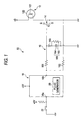
- Fig. 1 is a circuit diagram showing an incandescent lamp illumination circuit according to a first embodiment of the present invention
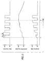
- Fig. 2 is a timing chart, showing a voltage waveform of a control signal output to a signal output terminal in the incandescent lamp illumination circuit shown in Fig. 1, a waveform of a voltage across a capacitor, a voltage waveform of a control signal appearing at a gate of a MOSFET; and
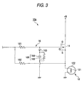
- Fig. 3 is a circuit diagram showing an incandescent lamp illumination circuit according to a second embodiment of the present invention.
- Fig. 1 is a circuit diagram showing the configuration of an incandescent lamp to which a method of illuminating an incandescent lamp according to a first embodiment of the present invention is applied.
- an incandescent lamp illumination circuit 10 is to be installed in a vehicle, such as an automobile, in the present embodiment.
- the illumination circuit 10 comprises an incandescent lamp 12; ann-channel MOSFET 14 which is a semicondllctor switching element having a control terminal and connected in series with the incandescent lamp 12; a signal level control section 16 for controlling operation of the MOSFET 14; and a control section 18 for supplying a control signal (i.e., a pulse signal) to the MOSFET 14 via the signal level control section 16.
- a control signal i.e., a pulse signal
- the incandescent lamp 12 is constituted by sheathing a filament 121 with a glass cladding 122.
- An inactive gas such as Argon gas, is sealed in the glass cladding 122, thereby preventing burning of the filament 121.
- One end of the filament 121 is connected to a +B terminal of a battery, and the other end of the filament 121 is connected to the MOSFET 14.
- the MOSFET 14 is of, e.g., enhanced type and has a drain D connected to the incandescent lamp 12, a source S connected to a ground which serves as a reference potential, and a gate G which is to act as a control terminal and is connected to the signal level control section 16.
- the signal level control section 16 controls a voltage level (voltage value) of a control signal supplied to the gate G of the MOSFET 14 so as to gradually increase from a low value to a higher value (a voltage level at the time of normal illumination).
- the signal level control section 16 comprises a first resistance element 161 interposed between the control section 18 and the gate G of the MOSFET 14; a second resistance element 162 interposed between the control section 18 and the source S of the MOSFET 14; a diode 163 whose anode is connected to the gate G of the MOSFET 14; and a CR parallel circuit 166 which is constituted of a combination of a capacitor 164 and a third resistance element 165 and is interposed between the cathode of the diode 163 and a ground serving as the reference potential.
- the first resistance element 161 prevents parasitic oscillation of the MOSFET 14, sets a charge time with respect to gate parasitic capacitance, and constitutes a time-constant circuit in conjunction with the capacitor 164.
- the second resistance element 162 is for discharging electric charge from the gate parasitic capacitance.
- the third resistance element 165 is for discharging electric charge accumulated in the capacitor 164.
- the diode 163 enables flow of an electric current from the gate G of the MOSFET 14 to the reference potential during only the ON period of a pulse signal output from the control section 18.
- the resistance value of the first resistance element 161, that of the third resistance element 165, and the electrostatic capacity of the capacitor 164 are set such that a time constant defined by the third resistance element 165 and the capacitor 164 becomes greater than that defined by the first resistance element 161 and the capacitor 165.
- the control section 18 comprises a microcomputer consisting of a CPU (central processing unit) for performing an arithmetic operation, ROM (read-only memory) having stored therein a processing program and various types of data, and RAM (random-access memory) for temporarily storing processed data.
- the microcomputer controls operation of a pulse generator 20, which serves as control signal supply means constituted of a multi-vibrator built in the control section 18.
- the control section 18 has a signal input terminal 18a into which an operation signal produced by an operation switch 22 of the incandescent lamp 12 is input, and a signal output terminal 18b which supplies a pulse signal of predetermined duty ratio produced by the pulse generator 20 to the gate G of the MOSFET 14 via the signal level control section 16.
- an illumination instruction signal produced as a result of activation of the operation switch 22 is input to the signal input terminal 18a of the control section 18.
- a control signal set to a predetermined duty ratio is output from the signal output terminal 18b.
- the control signal is supplied (applied) to the gate G of the MOSFET 16 via the signal level control section 16.
- the potential of the gate G is in a low state, because electric charge is not stored in the capacitor 164 at the beginning of output of an illumination instruction signal.
- a period of high level that is, during an ON period of the control signal, electric charge is gradually accumulated in the capacitor 164 via the diode 163, whereby the potential of the gate G gradually becomes high.
- Th electric charges stored in the capacitor 164 are discharged during a period of low level; that is, during an OFF period of the control signal via the third resistance element 165. Since the time constant defined by the third resistance element 165 and the capacitor 164 is greater than that defined by the first resistance element 161 and the capacitor 164, the capacitor 164 is recharged before starting substantial electric discharge. Presence of the diode 163 in the direction opposite to the capacitor 164 when viewed from the capacitor 164 hinders occurrence of electric discharge of the capacitor 164 via the first resistance element 161 and the second resistance element 162. Consequently, electric charges are effectively stored in the capacitor 164.
- the drain D and the source S are gradually brought into conduction, and an electric current gradually starts flowing into the filament 121 of the incandescent lamp 12.
- the MOSFET 14 is brought into normal conduction, and a specified electric current flows into the incandescent lamp 12.
- the incandescent lamp 12 enters a normal illuminated state. For this reason, there is prevented shortening of the life of the filament 121. Further, there is prevented occurrence of changes in supply voltage, which would in turn affect other device. Moreover, there is prevented wasteful dissipation of power, which would have been caused by the related-art thermistor. Hence, flow of an inrush current into the incandescent lamp 12 can be suppressed effectively.
- An extinction instruction signal generated as a result of deactivation of the operation switch 22 is input to the signal input terminal 18a of the control section 18. Output of the control signal from the signal output terminal 18 is stopped. Then, the electric charges stored in the capacitor 164 are discharged via the third resistance element 165, whereupon the potential of the gate G of the MOSF2T 14 drops gradually. Even when the illumination instruction signal is again input to the signal input terminal 18a, flow of an inrush current into the incandescent lamp 12 is effectively controlled, by means of operation of the signal level control section 16 in a phase in which electric discharge of the capacitor has been completed.
- the time constant of a CR parallel circuit 166 is set such that electric discharges is completed before a large drop has arisen in the temperature of the filament 121 of the incandescent lamp 12 as well as in the resistance of the filament 121. Even when the illumination instruction signal is again input to the signal input terminal 18a before completion of electric discharge, flow of a large in-rush current can be prevented by means of electrical resistance of the filament 121. As mentioned above, when the illumination instruction signal is output before completion of electric discharge, conduction of the MOSFET 14 is not much inhibited. For this reason, there can be prevented heating of the MOSFET 14, which would otherwise be caused by an increase in ON resistance between the drain and the source.
- Fig. 2 is a timing chart, showing a voltage waveform of a control signal (input voltage) output to the signal output terminal 18b of the control section 18; the waveform of a voltage developing across the capacitor 164 (capacitor voltage); and the waveform of voltage of a control signal (gate voltage) appearing in the gate G of the MOSFET 14.
- the potential developing across the capacitor 164 is zero. Hence, the potential of the gate G of the MOSFET 14 remains zero. Since the voltage across the capacitor 164 increases gradually, a voltage equal in magnitude with the potential across the capacitor 164 is supplied to the gate G of the MOSFET 14 during only a period of Ta in which the control signal remains in a high level. At time t2 at which recharging of the capacitor 164 is completed and in a subsequent phase, a voltage of specified value (e.g., 10V) appearing at the time of normal illumination of the incandescent lamp is supplied.
- a voltage of specified value e.g. 10V
- the potential across the capacitor 164 has a magnitude corresponding to the period of recharging time. Presence of the diode 163 in the direction opposite to the capacitor 164 when viewed from the capacitor 164 hinders supply of the voltage across the capacitor 164 to the gate G of the MOSFET 14. Hence, the potential of the gate G during the period Tb in which the control signal is in a low level becomes zero.
- the drain D and the source S of the MOSFET 14 are gradually brought into conduction with a gradual increase in the voltage level of the control signal supplied to the gate G (namely, a drain current corresponding to the magnitude of the control signal flows into the gate G). Hence, flow of a large inrush current into the incandescent lamp 12 at the beginning of energization is prevented.
- Fig. 3 is a circuit diagram showing the configuration of the incandescent lamp illumination circuit 10a according to a second embodiment of the present invention
- the incandescent lamp illumination circuit according to the present embodiment is identical in configuration with that shown in Fig. 1 and described in connection with the first embodiment, except that the incandescent lamp 12 is provided inthe reference voltage part of circuitry, and the MOSFET 14 is connected to the +B terminal.
- Those elements which are the same as the constituent elements shown in Fig. 1 are assigned the same reference numerals, and their detailed explanations are omitted. Even the incandescent lamp illumination circuit having the foregoing configuration yields completely the same working-effect as that yielded in the first embodiment shown in Fig. 1.
- a terminal of the CR parallel circuit 166 may be connected directly not to the reference potential but to the source S of the MOSFET 14 and further to the reference potential via the filament 121 of the incandescent lamp 12. Even in such a configuration, the incandescent lamp illumination circuit 10a operates completely in the same manner as in the case of the terminal of the CR parallel circuit 166, differing from the terminal of the same opposing the diode 163, is connected directly to the reference potential.
- the MOSFET 14 is gradually brought into conduction, by means of gradually increasing the voltage level of the control signal supplied to the gate G of the MOSFET 14 through use of the signal level control section 16, thereby suppressing conduction of the MOSFET 14 at the beginning of energization. Flow of an inrush current into the incandescent lamp can be suppressed effectively without involvement of wasteful power dissipation. In a normal illuminated state of the incandescent lamp, conduction of the MOSFET 14 is not suppressed.
- the voltage level of the control signal to be supplied to the control terminal is made lower than a voltage level obtained at the time of normal illumination of the incandescent lamp, at the beginning of energization of the incandescent lamp, thus inhibiting conduction of the semiconductor switch element. Flow of an inrush current into the incandescent lamp can be effectively inhibited without wasteful power dissipation.
Landscapes
- Circuit Arrangement For Electric Light Sources In General (AREA)
Applications Claiming Priority (2)
| Application Number | Priority Date | Filing Date | Title |
|---|---|---|---|
| JP2001007940A JP2002216979A (ja) | 2001-01-16 | 2001-01-16 | 白熱ランプの点灯方法及び白熱ランプの点灯回路 |
| JP2001007940 | 2001-01-16 |
Publications (2)
| Publication Number | Publication Date |
|---|---|
| EP1227704A2 true EP1227704A2 (de) | 2002-07-31 |
| EP1227704A3 EP1227704A3 (de) | 2005-09-07 |
Family
ID=18875616
Family Applications (1)
| Application Number | Title | Priority Date | Filing Date |
|---|---|---|---|
| EP02000811A Withdrawn EP1227704A3 (de) | 2001-01-16 | 2002-01-14 | Verfahren und Schaltung zum Betreiben einer Glühlampe |
Country Status (3)
| Country | Link |
|---|---|
| US (1) | US6518713B2 (de) |
| EP (1) | EP1227704A3 (de) |
| JP (1) | JP2002216979A (de) |
Cited By (2)
| Publication number | Priority date | Publication date | Assignee | Title |
|---|---|---|---|---|
| EP1816902A3 (de) * | 2006-02-06 | 2008-07-02 | Tyco Electronics Raychem GmbH | Strahlungsquelle für eine Sensoranordnung mit Einschaltstrombegrenzung |
| CN110446312A (zh) * | 2019-06-25 | 2019-11-12 | 杭州艾芯智能科技有限公司 | 一种关于提高光源性能的电路设计方法 |
Families Citing this family (5)
| Publication number | Priority date | Publication date | Assignee | Title |
|---|---|---|---|---|
| JP3793880B2 (ja) * | 2003-02-06 | 2006-07-05 | 松永 浩 | 点灯装置 |
| JP2008311187A (ja) * | 2007-06-18 | 2008-12-25 | Tokai Rika Co Ltd | ランプ駆動回路 |
| CN102231931A (zh) * | 2011-07-27 | 2011-11-02 | 宁波市鄞州赛艾富光电科技有限公司 | 一种led驱动装置 |
| CN105208748B (zh) * | 2015-10-27 | 2017-12-29 | 广西职业技术学院 | 一种逐级变亮的灯控装置 |
| US11863062B2 (en) * | 2018-04-27 | 2024-01-02 | Raytheon Company | Capacitor discharge circuit |
Family Cites Families (6)
| Publication number | Priority date | Publication date | Assignee | Title |
|---|---|---|---|---|
| US4570108A (en) * | 1982-07-06 | 1986-02-11 | Stroede Aake | Protection device for electrical incandescent lamps |
| US5283707A (en) * | 1992-11-27 | 1994-02-01 | Northern Telecom Limited | Inrush current limiting circuit |
| JP3470809B2 (ja) * | 1992-12-02 | 2003-11-25 | イーエムシー コーポレイション | インラッシュ電流リミッター |
| JPH08171813A (ja) | 1994-12-16 | 1996-07-02 | Matsushita Electric Ind Co Ltd | 白熱ランプ点灯装置 |
| US5631523A (en) * | 1995-09-19 | 1997-05-20 | Beacon Light Products, Inc. | Method of regulating lamp current through a fluorescent lamp by pulse energizing a driving supply |
| FI991042A7 (fi) * | 1999-05-06 | 2001-02-14 | Iws Int Oy | Ohjauspiiri jännite- ja virtapiikin poistamiseksi |
-
2001
- 2001-01-16 JP JP2001007940A patent/JP2002216979A/ja active Pending
-
2002
- 2002-01-14 EP EP02000811A patent/EP1227704A3/de not_active Withdrawn
- 2002-01-14 US US10/043,116 patent/US6518713B2/en not_active Expired - Fee Related
Cited By (3)
| Publication number | Priority date | Publication date | Assignee | Title |
|---|---|---|---|---|
| EP1816902A3 (de) * | 2006-02-06 | 2008-07-02 | Tyco Electronics Raychem GmbH | Strahlungsquelle für eine Sensoranordnung mit Einschaltstrombegrenzung |
| CN110446312A (zh) * | 2019-06-25 | 2019-11-12 | 杭州艾芯智能科技有限公司 | 一种关于提高光源性能的电路设计方法 |
| CN110446312B (zh) * | 2019-06-25 | 2022-02-18 | 杭州艾芯智能科技有限公司 | 一种关于提高光源性能的电路设计方法 |
Also Published As
| Publication number | Publication date |
|---|---|
| US20020093293A1 (en) | 2002-07-18 |
| JP2002216979A (ja) | 2002-08-02 |
| US6518713B2 (en) | 2003-02-11 |
| EP1227704A3 (de) | 2005-09-07 |
Similar Documents
| Publication | Publication Date | Title |
|---|---|---|
| CN101785118B (zh) | 驱动装置 | |
| EP3272585B1 (de) | Schalterantriebsvorrichtung, lichtemittierende vorrichtung und fahrzeug | |
| US20030007373A1 (en) | Switched-capacitor-type stabilized power supply device | |
| EP2736146A1 (de) | Antriebsaggregat eines fahrzeuges | |
| CN103402284A (zh) | 驱动装置、平滑电路、dc/dc变换器 | |
| JPH08289483A (ja) | 電源回路 | |
| US20070052471A1 (en) | Power Supply Apprartus | |
| JP7063297B2 (ja) | 車載電源装置 | |
| US6518713B2 (en) | Method of illuminating incandescent lamp, and circuit for illuminating the same | |
| KR910005113B1 (ko) | 간략화한 가스 방전장치 심머링 회로 및 이의 동작 방법 | |
| US6369513B1 (en) | Vehicle lamp lighting-driving apparatus | |
| US7196502B2 (en) | Switching regulator having soft start circuit | |
| US4727261A (en) | Multiple power FET vehicle lamp switch arrangement with charge pump sharing | |
| US6504316B2 (en) | Discharge lamp lighting circuit | |
| US20030107357A1 (en) | Vehicle electric power unit | |
| US10396660B2 (en) | Switching regulator, semiconductor integrated circuit, and electronic appliance | |
| JP2005026071A (ja) | 放電灯点灯回路 | |
| US6111365A (en) | Fast starting, surge limited, electronic ballast | |
| JP2021002440A (ja) | 点灯制御装置、点灯制御方法、車両用灯具 | |
| US8878385B2 (en) | Apparatus for controlling power supplied to discharge lamp in response to command supplied from outside the apparatus | |
| EP2219422B1 (de) | Entladungslampenlichtstromkreis mit einem Starterstromkreis | |
| JPH11329778A (ja) | 負荷の作動回路 | |
| JP2969286B2 (ja) | 放電灯点灯装置 | |
| WO2003059681A3 (de) | Schaltungsanordnung zur kurzzeitigen aufrechterhaltung wenigstens einer internen betriebs-gleichspannung beim ausfall der bordnetz-versorgungsspannung | |
| KR100236645B1 (ko) | 마이콤을 이용한 정전압 회로 |
Legal Events
| Date | Code | Title | Description |
|---|---|---|---|
| PUAI | Public reference made under article 153(3) epc to a published international application that has entered the european phase |
Free format text: ORIGINAL CODE: 0009012 |
|
| AK | Designated contracting states |
Kind code of ref document: A2 Designated state(s): AT BE CH CY DE DK ES FI FR GB GR IE IT LI LU MC NL PT SE TR |
|
| AX | Request for extension of the european patent |
Free format text: AL;LT;LV;MK;RO;SI |
|
| PUAL | Search report despatched |
Free format text: ORIGINAL CODE: 0009013 |
|
| AK | Designated contracting states |
Kind code of ref document: A3 Designated state(s): AT BE CH CY DE DK ES FI FR GB GR IE IT LI LU MC NL PT SE TR |
|
| AX | Request for extension of the european patent |
Extension state: AL LT LV MK RO SI |
|
| AKX | Designation fees paid | ||
| STAA | Information on the status of an ep patent application or granted ep patent |
Free format text: STATUS: THE APPLICATION IS DEEMED TO BE WITHDRAWN |
|
| 18D | Application deemed to be withdrawn |
Effective date: 20050308 |
|
| REG | Reference to a national code |
Ref country code: DE Ref legal event code: 8566 |