EP1228633B1 - Digitales photographisches wiedergabegerät - Google Patents
Digitales photographisches wiedergabegerät Download PDFInfo
- Publication number
- EP1228633B1 EP1228633B1 EP00971552A EP00971552A EP1228633B1 EP 1228633 B1 EP1228633 B1 EP 1228633B1 EP 00971552 A EP00971552 A EP 00971552A EP 00971552 A EP00971552 A EP 00971552A EP 1228633 B1 EP1228633 B1 EP 1228633B1
- Authority
- EP
- European Patent Office
- Prior art keywords
- light
- optical
- face
- receiving face
- light receiving
- Prior art date
- Legal status (The legal status is an assumption and is not a legal conclusion. Google has not performed a legal analysis and makes no representation as to the accuracy of the status listed.)
- Expired - Lifetime
Links
Images

Classifications
-
- H—ELECTRICITY
- H04—ELECTRIC COMMUNICATION TECHNIQUE
- H04N—PICTORIAL COMMUNICATION, e.g. TELEVISION
- H04N1/00—Scanning, transmission or reproduction of documents or the like, e.g. facsimile transmission; Details thereof
- H04N1/04—Scanning arrangements, i.e. arrangements for the displacement of active reading or reproducing elements relative to the original or reproducing medium, or vice versa
- H04N1/19—Scanning arrangements, i.e. arrangements for the displacement of active reading or reproducing elements relative to the original or reproducing medium, or vice versa using multi-element arrays
- H04N1/191—Scanning arrangements, i.e. arrangements for the displacement of active reading or reproducing elements relative to the original or reproducing medium, or vice versa using multi-element arrays the array comprising a one-dimensional [1D] array
- H04N1/192—Simultaneously or substantially simultaneously scanning picture elements on one main scanning line
- H04N1/193—Simultaneously or substantially simultaneously scanning picture elements on one main scanning line using electrically scanned linear arrays, e.g. linear CCD arrays
- H04N1/1935—Optical means for mapping the whole or part of a scanned line onto the array
- H04N1/1936—Optical means for mapping the whole or part of a scanned line onto the array using a light guide, e.g. an optical fibre bundle or array
-
- B—PERFORMING OPERATIONS; TRANSPORTING
- B41—PRINTING; LINING MACHINES; TYPEWRITERS; STAMPS
- B41J—TYPEWRITERS; SELECTIVE PRINTING MECHANISMS, i.e. MECHANISMS PRINTING OTHERWISE THAN FROM A FORME; CORRECTION OF TYPOGRAPHICAL ERRORS
- B41J2/00—Typewriters or selective printing mechanisms characterised by the printing or marking process for which they are designed
- B41J2/435—Typewriters or selective printing mechanisms characterised by the printing or marking process for which they are designed characterised by selective application of radiation to a printing material or impression-transfer material
- B41J2/447—Typewriters or selective printing mechanisms characterised by the printing or marking process for which they are designed characterised by selective application of radiation to a printing material or impression-transfer material using arrays of radiation sources
- B41J2/455—Typewriters or selective printing mechanisms characterised by the printing or marking process for which they are designed characterised by selective application of radiation to a printing material or impression-transfer material using arrays of radiation sources using laser arrays, the laser array being smaller than the medium to be recorded
-
- B—PERFORMING OPERATIONS; TRANSPORTING
- B41—PRINTING; LINING MACHINES; TYPEWRITERS; STAMPS
- B41J—TYPEWRITERS; SELECTIVE PRINTING MECHANISMS, i.e. MECHANISMS PRINTING OTHERWISE THAN FROM A FORME; CORRECTION OF TYPOGRAPHICAL ERRORS
- B41J2/00—Typewriters or selective printing mechanisms characterised by the printing or marking process for which they are designed
- B41J2/435—Typewriters or selective printing mechanisms characterised by the printing or marking process for which they are designed characterised by selective application of radiation to a printing material or impression-transfer material
- B41J2/447—Typewriters or selective printing mechanisms characterised by the printing or marking process for which they are designed characterised by selective application of radiation to a printing material or impression-transfer material using arrays of radiation sources
- B41J2/46—Typewriters or selective printing mechanisms characterised by the printing or marking process for which they are designed characterised by selective application of radiation to a printing material or impression-transfer material using arrays of radiation sources characterised by using glass fibres
-
- G—PHYSICS
- G02—OPTICS
- G02B—OPTICAL ELEMENTS, SYSTEMS OR APPARATUS
- G02B6/00—Light guides; Structural details of arrangements comprising light guides and other optical elements, e.g. couplings
- G02B6/24—Coupling light guides
- G02B6/42—Coupling light guides with opto-electronic elements
- G02B6/4201—Packages, e.g. shape, construction, internal or external details
- G02B6/4249—Packages, e.g. shape, construction, internal or external details comprising arrays of active devices and fibres
-
- H—ELECTRICITY
- H04—ELECTRIC COMMUNICATION TECHNIQUE
- H04N—PICTORIAL COMMUNICATION, e.g. TELEVISION
- H04N1/00—Scanning, transmission or reproduction of documents or the like, e.g. facsimile transmission; Details thereof
- H04N1/04—Scanning arrangements, i.e. arrangements for the displacement of active reading or reproducing elements relative to the original or reproducing medium, or vice versa
- H04N1/19—Scanning arrangements, i.e. arrangements for the displacement of active reading or reproducing elements relative to the original or reproducing medium, or vice versa using multi-element arrays
- H04N1/191—Scanning arrangements, i.e. arrangements for the displacement of active reading or reproducing elements relative to the original or reproducing medium, or vice versa using multi-element arrays the array comprising a one-dimensional [1D] array
- H04N1/192—Simultaneously or substantially simultaneously scanning picture elements on one main scanning line
- H04N1/193—Simultaneously or substantially simultaneously scanning picture elements on one main scanning line using electrically scanned linear arrays, e.g. linear CCD arrays
Definitions
- This invention relates to digital photographic reproduction apparatus for producing a photographic image from digital image data.
- Digital photographic printing systems for this purpose are available commercially and are known commonly as photographic paperwriters. However such systems are costly and this renders their use uneconomical in many photoprocessing outlets.
- One type of photographic paperwriter which is commercially available makes use of a lens system to focus laser beams modulated by the digital data onto standard photographic paper in order to produce photographic colour prints at a rate of up to a thousand 8 X 10 inch prints per hour. However such equipment is large, complex and very expensive.
- GB 2042746A discloses a multiple variable light source for a photographic printer incorporating an array of light-emitting diodes and a respective optical fibre associated with each light-emitting diode for conducting light from the diode towards the surface of a photoconductive drum.
- each individual fibre must have its end correctly aligned with respect to the associated light-emitting diode if acceptable photographic quality is to be achieved.
- Similar types of fibre optical array suffering from the same disadvantage, are disclosed in WO 90/04194 and WO 90/04195.
- digital photographic reproduction apparatus for producing a photographic image from digital image data
- the apparatus comprising carrier means for receiving a suitable photographic image carrier medium, an optical light pipe having a light receiving face at one end and a light transmitting face at an opposite end arranged to lie adjacent to the carrier medium, an array of light-emitting devices arranged adjacent the light receiving face of the light pipe, and digital control means for controlling the light-emitting devices so as to supply, in response to digital image data, optical writing signals which are transmitted along the light pipe to the carrier medium to produce a photographic image on the carrier medium, characterised in that the light pipe comprises a solid coherent bundle of optical fibres which is tapered in a region between the light receiving face and the light transmitting face so that the light receiving face has a substantially greater surface area than the light transmitting face to thereby increase the optical resolution of the photographic image.
- Such digital photographic reproduction apparatus can be produced at much lower cost than currently commercially available systems, and can rapidly and accurately expose photographic paper to a digitally controlled image with a high degree of resolution, that is with a spot size of the order of 1/200 to 1 / 800 of an inch (120 to 30 ⁇ m).
- Document WO-A-97/42560 discloses a solid coherent bundle of optical fibres which is tapered in a region between the light receiving face and the light transmitting face.
- optical and light as used in this specification are not intended to be limited simply to electromagnetic radiation in the visible part of the spectrum, and these terms are also to be considered as embracing within their scope electromagnetic radiation outside the visible part of the spectrum, such as infrared or ultraviolet light.
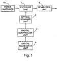
- the digital photographic printing apparatus shown diagrammatically in Figure 1 comprises a photographic paper exposure unit 1 for receiving a sheet of photographic paper from a paper cartridge 1A and for feeding the sheet past the writing head of an optical scanner unit 2.
- the writing head incorporates an array of light-emitting devices which are controlled by signals from a digital controller unit 3 which incorporates sample and hold circuitry for holding successive sets of partial image data received from a digital image data unit 4 and for controlling the light-emitting devices during successive time periods to build up the photographic image a part at a time.
- the sheet is moved past the optical scanner unit 2 by the carrier unit 1, successive portions of the sheet are optically exposed to the writing head and to an optical image determined by the control of the light-emitting devices by the digital controller unit 3 in accordance with the applied digital image data.
- the sheet is passed to a developer unit 5 within which developing is effected by a wet development process prior to the developed sheet being outputted by the apparatus.
- the developer unit is preferably an integral part of the apparatus to which the sheet is automatically supplied by the carrier unit 1 after exposure, it would also be possible for the developer unit to form a separate item of apparatus to which the sheet is manually transferred by the user after exposure.
- the apparatus is based around existing bubble-jet printer technology with the ink cartridge and the printing head being replaced by an optical writing head so that raster scanning of the photographic paper sheet occurs as the sheet is moved stepwise in a direction transverse to the direction along which the optical writing head is moved along each line.
- Such raster scanning could be performed by an arrangement in which the sheet is held stationary on the carrier platen whilst the optical writing head is scanned over the sheet a line at a time with the writing head being displaced, between writing of each line, by one step transversely of the line.
- the optical writing head of such digital photographic printing apparatus comprises a light pipe in the form of a solid fused bundle 10 of coherent optical fibres having a central optical axis 11, as shown diagrammatically from the side in Figure 2.
- a light transmitting face 12 of the optical fibre bundle 10 is cut and polished normal to the axis 11, and a light receiving face 13 of the optical fibre bundle 10 is also cut and polished normal to the axis 11.
- the optical fibre bundle 10 incorporates a tapered region 17 in which the individual optical fibres have been drawn so as to progressively decrease their diameters, as well as an untapered input region 18 in which the optical fibres are of a constant maximum diameter and an untapered output region 19 in which the optical fibres are of a constant minimum diameter.
- an array of light-emitting or laser diodes 14 is attached to a printed circuit board 15 positioned adjacent to, and extending parallel to, the light receiving face 13 of the optical fibre bundle 10 such that good light transmission between the diodes 14 and the optical fibre bundle 10 is achieved.
- the array of light-emitting or laser diodes 14 comprises three linear arrays, that is an array 20 of red diodes 14, an array 21 of green diodes 14, and an array 22 of blue diodes 14, mounted side-by-side on the printed circuit board 15, as shown from the front in the diagram of Figure 3.
- any number of linear arrays may be used in such an optical writing head, and that colours other than red, green and blue may be used in these arrays.
- the colours (or spectra ) of the particular light-emitting diodes used will have to be chosen for the particular photographic paper used.
- the electrical connectors 23 by means of which the switching signals are supplied to the three arrays 20, 21, 22 by the digital controller unit.
- the emitted light travels down the fibres of the optical fibre bundle 10 and is emitted from the light transmitting face 12 as indicated by the arrows 16. It will be appreciated that, when the light transmitting face 12 is viewed from A, the diodes 14 of the array adjacent the light receiving face 13 of the optical bundle 10 appear as though positioned closer together so that, when all the diodes are illuminated, an array of light spots 30 is seen, as shown in the diagrammatic end view of the light transmitting face 12 of Figure 4.
- the image reduction can be expressed as a ratio D1 : D2 where D1 is the diameter of the light receiving face 13 and D2 is the diameter of the light transmitting face 12 of the optical fibre bundle 10.
- Calculations show that, in order to produce light spots having a desired resolution (spot size) of 60 ⁇ m with an array of diodes 14 spaced apart by 0.3mm, it is necessary for the tapered region 17 to produce a 5 : 1 image reduction. Greater resolution can be achieved by reducing the spacing of the diodes 14 or by increasing the reduction ratio of the tapered region 17. If the coupling efficiency of light from the diodes 14 into the optical fibre bundle 10 is of the order of 7%, the light output of the optical fibre bundle 10 is sufficient to expose photographic paper at an acceptable rate.
- three parallel linear arrays 20, 21 and 22 of diodes 14 are positioned adjacent the light receiving face 13 of the optical fibre bundle 10, the three linear arrays being placed next to each other on a single optical fibre bundle, and the three arrays of diodes being controlled with appropriate electronic delays during raster scanning so as to align the red, green and blue images, in a manner similar to that used in conventional bubble-jet printers.
- the raster scanning of the photographic paper by the optical writing head normal to the linear arrays 20, 21, 22 is shown diagrammatically at 24 in Figure 3.
- raster scanning occurs along a direction which is not normal to the linear arrays, but which extends along at a non-normal angle, for example 45°, to the linear arrays.
- the optical fibre bundle 10 may include interstitial material between the individual optical fibres so as to reduce inter-element optical crosstalk. Furthermore it may be advantageous for the diameter of the optical fibres at the light receiving face 13 (the maximum optical fibre diameter) to be chosen to be less than one quarter of the size of the light-emitting diodes in order to reduce speckle noise in the final image. Whilst other types of light-emitting device can be used in the optical writing head, it is considered that light-emitting diodes are particularly suitable for this application since they are relatively inexpensive, are efficient at converting electrical energy into coloured light, can be switched very rapidly and are easily fabricated into small linear arrays. Furthermore they can be chosen to have output wavelengths which are particularly desirable in this application.
- Colour filters may be added (either as discrete elements, or in the form of a dye added to the LED encapsulant) to modify the spectral output from the light-emitting diodes. Because of the reduction in size of the image, the precise alignment of the diodes on the printed circuit board is not critical, and this is a significant factor in simplifying the manufacturing process.
- Figure 5 shows a portion of the light receiving face 13 of the optical fibre bundle 10 on an enlarged scale, showing in particular the positioning of the light-emitting diodes 14 relative to the ends 31 of the individual optical fibres at the light receiving face 13.
- an anti-reflection coating 32 may be applied to the light receiving face 13 in order to reduce reflection losses.
- an anti-reflection coating may be applied to the light transmitting face 12 of the optical fibre bundle 10.
- a transparent encapsulating layer 33 which is applied to the face of the printed circuit board 15 on which the light-emitting diodes 14 are mounted in order to protect the fragile connecting wires 34 of the diodes.
- the presence of the encapsulating layer 33 means that there must be a finite spacing between the diodes 14 and the light receiving face 13 of the fibre optic bundle 10.
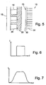
- the light coupling in order to make the optical image more pleasing to the eye, it is desirable to arrange for the light coupling to be such that the image spots do not have a square intensity profile as shown in Figure 6, where I represents the light intensity and d represents the distance of each point along a line from a reference point outside the light spot. Instead it is desirable for the image spots to have an intensity profile as shown in Figure 7 in which the intensity falls off gradually at the edges of each spot.
- Such smoothing can be controlled by accurately maintaining the distance between the diodes and the light receiving face 13 over the whole area of the light receiving face 13. Accurate control of this distance will allow sufficient light from each diode to fall on the surrounding optical fibres so as to reduce the desired degree of light spreading in its image on the photographic paper.
- a light source other than light-emitting or laser diodes such as a white light source and an associated liquid crystal light modulator. Since the power output determines the speed at which light exposure of the sheet can be effected, particular attention must be paid to providing a light source of adequate power output. It may also be appropriate in certain applications to provide optical signal processing so that the illumination of the diodes is controlled in such a manner as to compensate for scanning inhomogeneities and/or differences in light responsiveness.
- the image printed onto the photographic paper would consist of a square array of dots.
- the dots formed along alternate print lines may be shifted by one half of the dot spacing with the result that a hexagonal array of dots is produced.
- Such a hexagonal array allows the dots to pack together with a smaller gap or overlap area than with the square array so that, for the same size of dot, the resolution and number of dots per unit area can be increased.
- the required shifting between alternate lines may be achieved by shifting the head under the control of a piezoelectric crystal.
- the light source is controlled so as to be turned rapidly on and off at a frequency and with an on/off ratio such that the required brightness is obtained over the activation period.
- the brightness of the red, green and blue components of the colour image may be varied relative to one another to redistribute the quantisation noise.
- This technique can also be used to prevent the occurrence of Moiré patterns in the image due to beat frequencies between superimposed patterns. Further reduction in Moiré and quantisation noise patterns may be achieved by dithering the dot position by applying a random signal to the piezoelectric crystal used to control shifting between alternate lines in production of the hexagonal array as described above.
- the optical transducer in accordance with the invention may be used in a variety of applications for writing (and optionally also reading) of data on a suitable data carrier medium.
- the light sources may or may not be formed by diode arrays, and the light compression may be effected using a single fibre optic bundle, or alternatively using two fibre optic bundles in sequence for compression in two directions transverse to one another.
- One possible further application is reading/writing onto compact disks using a large number of heads in order to speed up the reading/writing process.
- the apparatus is also suitable for the production of photographic negatives or transparencies from digital data image data in which case a photographic image may be produced at a higher resolution than in a photographic print.
Landscapes
- Physics & Mathematics (AREA)
- Optics & Photonics (AREA)
- Health & Medical Sciences (AREA)
- Engineering & Computer Science (AREA)
- Multimedia (AREA)
- Signal Processing (AREA)
- General Health & Medical Sciences (AREA)
- Toxicology (AREA)
- General Physics & Mathematics (AREA)
- Printers Or Recording Devices Using Electromagnetic And Radiation Means (AREA)
- Projection-Type Copiers In General (AREA)
- Photographic Developing Apparatuses (AREA)
- Facsimile Scanning Arrangements (AREA)
- Forging (AREA)
- Light Receiving Elements (AREA)
- Steroid Compounds (AREA)
Claims (13)
- Digitale fotografische Reproduktionsvorrichtung zum Erzeugen eines fotografischen Bilds aus digitalen Bilddaten, wobei die Vorrichtung umfasst: eine Trägereinrichtung (1) zum Empfangen eines geeigneten fotografischen Bildträgermediums, ein optisches Lichtrohr (10) mit einer Lichtempfangsstimfläche (13) an einem Ende und einer Lichttransmissionsstimfläche (12) an einem gegenüberliegenden Ende, angeordnet, um angrenzend zu dem Trägermedium zu liegen, ein Feld von Licht-emittierenden Einrichtungen (14), die angrenzend zu der Lichtempfangsstimfläche (13) des Lichtrohrs (11) angeordnet sind, und eine digitale Steuereinrichtung (3) zum Steuern der Licht-emittierenden Einrichtungen (14), um so im Ansprechen auf digitale Bilddaten optische Schreibsignale zuzuführen, die entlang des Lichtrohrs (10) an das Trägermedium übertragen werden, um ein fotografisches Bild auf dem Trägermedium zu erzeugen, dadurch gekennzeichnet, dass das Lichtrohr (10) ein festes kohärentes Bündel von optischen Fasern umfasst, die in einem Bereich (17) zwischen der Lichtempfangsstirnfläche (13) und der Lichttransmissionsstimfläche (12) verjüngt ist, so dass die Lichtempfangsstirnfläche (13) eine wesentliche größere Oberfläche als die Lichttransmissionsstirnfläche (12) aufweist, um dadurch die optische Auflösung des fotografischen Bilds zu erhöhen.
- Vorrichtung nach Anspruch 1, wobei das optische Faserbündel (10) einen Bereich (18, 19) aufweist, in dem es nicht verjüngt ist und der zwischen dem verjüngten Bereich (17) und der Lichtempfangsstirnfläche (13) oder der Lichttransmissionsoberfläche (12) liegt.
- Vorrichtung nach Anspruch 2, wobei das optische Faserbündel (10) einen Bereich (18), in dem es nicht zwischen dem verjüngten Bereich (17) und der Lichtempfangsstirnfläche (13) verjüngt ist, und einen weiteren Bereich (19) aufweist, in dem es nicht zwischen dem verjüngten Abschnitt (17) und der Lichttransmissionsstirnfläche (12) verjüngt ist.
- Vorrichtung nach Anspruch 1, 2 oder 3, wobei die Licht-emittierenden Einrichtungen (14) drei lineare Felder von Licht-emittierenden Einrichtungen (20, 21, 22) zum Emittieren von optischen Schreibsignalen von drei unterschiedlichen Farben, geeignet zum Erzeugen eines Farbbilds auf dem Trägermedium, umfassen.
- Vorrichtung nach Anspruch 1, 2, 3 oder 4, wobei die Licht-emittierenden Einrichtungen (14) an einer gedruckten Schaltungsplatine (15) angebracht sind, die sich parallel zu der Lichtempfangsstirnfläche (13) des optischen Faserbündels (10) erstreckt.
- Vorrichtung nach irgendeinem vorangehenden Anspruch, wobei die Licht-emittierenden Einrichtungen (14) in einem vorgegebenen konstanten Abstand von der Lichtempfangsstirnfläche (13) des optischen Faserbündels (10) liegen, um die Spreizung des Lichts von den Einrichtungen (14), das auf die Lichtempfangsstimfläche (13) fällt, zu steuern.
- Vorrichtung nach irgendeinem vorangehenden Anspruch, wobei eine Anti-Reflektionsbeschichtung (32) auf der Lichtempfangsstimfläche (13) oder der Lichttransmissionsstirnfläche (12) des optischen Faserbündels (10) angebracht ist, um Reflektionsverluste zu begrenzen.
- Vorrichtung nach irgendeinem vorangehenden Anspruch, wobei das optische Faserbündel (10) entlang von zwei zueinander transversalen Ebenen zwischen der Lichtempfangsstirnfläche (13) und der Lichttransmissionsstirnfläche (12) verjüngt ist.
- Vorrichtung nach irgendeinem vorangehenden Anspruch, die dafür ausgelegt ist, um ein fotografisches Bild mit einer Auflösung in dem Bereich 10 bis 150 µm und vorzugsweise zwischen 30 und 60 µm zu erzeugen.
- Vorrichtung nach irgendeinem vorangehenden Anspruch, wobei die digitale Steuereinrichtung (3) eine Abtast- und Halte-Einrichtung zum Halten von sukzessiven Sätzen von Teilbilddaten und zum Steuern der Licht-emittiezenden Einrichtungen während sukzessiver Zeitperioden in Abhängigkeit von den Sätzen von Daten so, dass das fotografische Bild mit einem Teil zu einer Zeit aufgebaut wird, beinhaltet.
- Vorrichtung nach irgendeinem vorangehenden Anspruch, wobei eine Scan-Einrichtung (2) vorgesehen ist, um das fotografische Bild durch Scannen des Trägermediums durch die optischen Schreibsignale, die entlang des Lichtrohrs (10) geführt werden, zu erzeugen.
- Vorrichtung nach Anspruch 11, wobei die Scan-Einrichtung (2) dafür ausgelegt ist, um das Trägermedium durch die Vorrichtung in einer Richtung während der Anbringung des fotografischen Bilds auf das Trägermedium durch eine wiederholte Bewegung des Lichtrohrs (10) relativ zu dem Medium transversal zu der besagten einen Richtung zu bewegen.
- Vorrichtung nach irgendeinem vorangehenden Anspruch, wobei eine Entwicklungseinrichtung (5) vorgesehen ist, um das fotografische Bild, das an dem Trägermedium angebracht ist, chemisch zu entwickeln.
Applications Claiming Priority (3)
| Application Number | Priority Date | Filing Date | Title |
|---|---|---|---|
| GBGB9926394.9A GB9926394D0 (en) | 1999-11-09 | 1999-11-09 | Digital photographic reproduction apparatus |
| GB9926394 | 1999-11-09 | ||
| PCT/GB2000/004077 WO2001035633A1 (en) | 1999-11-09 | 2000-10-24 | Digital photographic reproduction apparatus |
Publications (2)
| Publication Number | Publication Date |
|---|---|
| EP1228633A1 EP1228633A1 (de) | 2002-08-07 |
| EP1228633B1 true EP1228633B1 (de) | 2004-03-03 |
Family
ID=10864141
Family Applications (1)
| Application Number | Title | Priority Date | Filing Date |
|---|---|---|---|
| EP00971552A Expired - Lifetime EP1228633B1 (de) | 1999-11-09 | 2000-10-24 | Digitales photographisches wiedergabegerät |
Country Status (6)
| Country | Link |
|---|---|
| US (1) | US6778738B1 (de) |
| EP (1) | EP1228633B1 (de) |
| AT (1) | ATE261224T1 (de) |
| DE (1) | DE60008781T2 (de) |
| GB (1) | GB9926394D0 (de) |
| WO (1) | WO2001035633A1 (de) |
Cited By (1)
| Publication number | Priority date | Publication date | Assignee | Title |
|---|---|---|---|---|
| US8446440B2 (en) | 2006-05-30 | 2013-05-21 | Lumejet Holdings Limited | Optical printers |
Families Citing this family (4)
| Publication number | Priority date | Publication date | Assignee | Title |
|---|---|---|---|---|
| GB9926394D0 (en) | 1999-11-09 | 2000-01-12 | Univ Warwick | Digital photographic reproduction apparatus |
| CN101187684B (zh) * | 2006-11-15 | 2011-06-22 | 鸿富锦精密工业(深圳)有限公司 | 主板发光二极管测试装置及方法 |
| GB2500365A (en) | 2012-02-01 | 2013-09-25 | Lumejet Holdings Ltd | Radiating device and print media exposure device |
| GB201209142D0 (en) * | 2012-05-24 | 2012-07-04 | Lumejet Holdings Ltd | Media exposure device |
Family Cites Families (13)
| Publication number | Priority date | Publication date | Assignee | Title |
|---|---|---|---|---|
| GB2042746A (en) | 1979-02-23 | 1980-09-24 | Savin Corp | Multiple Variable Light Source Photographic Printer |
| NL8103599A (nl) | 1981-07-30 | 1983-02-16 | Philips Nv | Inrichting voor het optisch aftasten van een document. |
| JPS5911065A (ja) * | 1982-07-10 | 1984-01-20 | Nippon Telegr & Teleph Corp <Ntt> | カラ−走査装置 |
| FR2601787A1 (fr) * | 1986-07-16 | 1988-01-22 | Primat Didier | Dispositif de tracage optique multivoie |
| US4763975A (en) * | 1987-04-28 | 1988-08-16 | Spectra Diode Laboratories, Inc. | Optical system with bright light output |
| JPS6411464A (en) | 1987-07-03 | 1989-01-17 | Mitsubishi Cable Ind Ltd | Exposure head for color scanner |
| US4911526A (en) | 1988-10-07 | 1990-03-27 | Eastman Kodak Company | Fiber optic array |
| US4923275A (en) | 1988-10-07 | 1990-05-08 | Eastman Kodak Company | Fiber optic array |
| US5117245A (en) * | 1990-01-22 | 1992-05-26 | Photon Imaging Corp. | Electronic printer or scanner using a fiber optic bundle and an array light emission device |
| GB9221813D0 (en) | 1992-10-16 | 1992-12-02 | Univ Montfort | Imaging arrangements |
| US5764845A (en) * | 1993-08-03 | 1998-06-09 | Fujitsu Limited | Light guide device, light source device, and liquid crystal display device |
| WO1997042560A1 (en) | 1996-05-09 | 1997-11-13 | Via, Inc. | Miniature display devices and systems |
| GB9926394D0 (en) | 1999-11-09 | 2000-01-12 | Univ Warwick | Digital photographic reproduction apparatus |
-
1999
- 1999-11-09 GB GBGB9926394.9A patent/GB9926394D0/en not_active Ceased
-
2000
- 2000-10-24 DE DE2000608781 patent/DE60008781T2/de not_active Expired - Lifetime
- 2000-10-24 US US10/129,638 patent/US6778738B1/en not_active Expired - Lifetime
- 2000-10-24 WO PCT/GB2000/004077 patent/WO2001035633A1/en not_active Ceased
- 2000-10-24 AT AT00971552T patent/ATE261224T1/de not_active IP Right Cessation
- 2000-10-24 EP EP00971552A patent/EP1228633B1/de not_active Expired - Lifetime
Cited By (1)
| Publication number | Priority date | Publication date | Assignee | Title |
|---|---|---|---|---|
| US8446440B2 (en) | 2006-05-30 | 2013-05-21 | Lumejet Holdings Limited | Optical printers |
Also Published As
| Publication number | Publication date |
|---|---|
| DE60008781T2 (de) | 2005-01-13 |
| WO2001035633A1 (en) | 2001-05-17 |
| ATE261224T1 (de) | 2004-03-15 |
| GB9926394D0 (en) | 2000-01-12 |
| DE60008781D1 (de) | 2004-04-08 |
| US6778738B1 (en) | 2004-08-17 |
| EP1228633A1 (de) | 2002-08-07 |
Similar Documents
| Publication | Publication Date | Title |
|---|---|---|
| EP0325366B1 (de) | Optisches Kommunikationssystem mehrerer Kanäle | |
| US6342960B1 (en) | Wavelength division multiplex transmitter | |
| US6239421B1 (en) | Rod lens array and image read apparatus and system using the same | |
| KR100300278B1 (ko) | 광학디바이스및화상판독장치 | |
| JPH08304706A (ja) | 空間光変調器のためのイルミネーション光学 | |
| US20070057151A1 (en) | Contact image sensor and method for manufacturing the same | |
| JP2001343531A (ja) | 照明装置、この照明装置を有するイメージセンサーおよびこのイメージセンサーを用いた画像読取装置ならびに情報処理システム | |
| US4220978A (en) | Electro-optical document reader | |
| EP1228633B1 (de) | Digitales photographisches wiedergabegerät | |
| US4517608A (en) | Image recording device | |
| US5965870A (en) | Image reading system with means for converging light from a plurality of light sources on a substantially same position to uniformly irradiate an object | |
| WO1980002467A1 (en) | Laser-based image recording system | |
| CA2008748A1 (en) | Integral fiber optic printhead | |
| US6760121B1 (en) | Beam scanning printer | |
| US5796907A (en) | Optical transmission line optical transmitter, and photographic printing apparatus | |
| US6535271B1 (en) | Exposure apparatus | |
| US7190483B2 (en) | Image recorder | |
| US6462841B1 (en) | Image sensor, and image processing apparatus using the same | |
| US6233001B1 (en) | Image recording apparatus | |
| US6549226B1 (en) | Optical printer head | |
| JP2574927B2 (ja) | レーザプリンタ用光ヘッド | |
| EP0809818A1 (de) | Leuchtdiode für optischen drucker mit effizienter lichtkegelcharakteristik | |
| KR20020044567A (ko) | 렌즈 어레이, 이미지 센서, 이 이미지 센서를 이용한 정보처리 장치 및 정보 처리 시스템 | |
| Tamura | Development of a multibeam recording head with laser diodes for color scanners | |
| JPS6014221A (ja) | 光変調方法及び光変調素子 |
Legal Events
| Date | Code | Title | Description |
|---|---|---|---|
| PUAI | Public reference made under article 153(3) epc to a published international application that has entered the european phase |
Free format text: ORIGINAL CODE: 0009012 |
|
| 17P | Request for examination filed |
Effective date: 20020529 |
|
| AK | Designated contracting states |
Kind code of ref document: A1 Designated state(s): AT BE CH CY DE DK ES FI FR GB GR IE IT LI LU MC NL PT SE |
|
| AX | Request for extension of the european patent |
Free format text: AL;LT;LV;MK;RO;SI |
|
| RAP1 | Party data changed (applicant data changed or rights of an application transferred) |
Owner name: DIG-EPRINT LIMITED |
|
| 17Q | First examination report despatched |
Effective date: 20020904 |
|
| GRAH | Despatch of communication of intention to grant a patent |
Free format text: ORIGINAL CODE: EPIDOS IGRA |
|
| GRAS | Grant fee paid |
Free format text: ORIGINAL CODE: EPIDOSNIGR3 |
|
| GRAA | (expected) grant |
Free format text: ORIGINAL CODE: 0009210 |
|
| AK | Designated contracting states |
Kind code of ref document: B1 Designated state(s): AT BE CH CY DE DK ES FI FR GB GR IE IT LI LU MC NL PT SE |
|
| PG25 | Lapsed in a contracting state [announced via postgrant information from national office to epo] |
Ref country code: FI Free format text: LAPSE BECAUSE OF FAILURE TO SUBMIT A TRANSLATION OF THE DESCRIPTION OR TO PAY THE FEE WITHIN THE PRESCRIBED TIME-LIMIT Effective date: 20040303 Ref country code: CY Free format text: LAPSE BECAUSE OF FAILURE TO SUBMIT A TRANSLATION OF THE DESCRIPTION OR TO PAY THE FEE WITHIN THE PRESCRIBED TIME-LIMIT Effective date: 20040303 Ref country code: AT Free format text: LAPSE BECAUSE OF FAILURE TO SUBMIT A TRANSLATION OF THE DESCRIPTION OR TO PAY THE FEE WITHIN THE PRESCRIBED TIME-LIMIT Effective date: 20040303 Ref country code: NL Free format text: LAPSE BECAUSE OF FAILURE TO SUBMIT A TRANSLATION OF THE DESCRIPTION OR TO PAY THE FEE WITHIN THE PRESCRIBED TIME-LIMIT Effective date: 20040303 Ref country code: LI Free format text: LAPSE BECAUSE OF FAILURE TO SUBMIT A TRANSLATION OF THE DESCRIPTION OR TO PAY THE FEE WITHIN THE PRESCRIBED TIME-LIMIT Effective date: 20040303 Ref country code: CH Free format text: LAPSE BECAUSE OF FAILURE TO SUBMIT A TRANSLATION OF THE DESCRIPTION OR TO PAY THE FEE WITHIN THE PRESCRIBED TIME-LIMIT Effective date: 20040303 Ref country code: BE Free format text: LAPSE BECAUSE OF FAILURE TO SUBMIT A TRANSLATION OF THE DESCRIPTION OR TO PAY THE FEE WITHIN THE PRESCRIBED TIME-LIMIT Effective date: 20040303 |
|
| REG | Reference to a national code |
Ref country code: GB Ref legal event code: FG4D |
|
| REG | Reference to a national code |
Ref country code: CH Ref legal event code: EP |
|
| REG | Reference to a national code |
Ref country code: IE Ref legal event code: FG4D |
|
| REF | Corresponds to: |
Ref document number: 60008781 Country of ref document: DE Date of ref document: 20040408 Kind code of ref document: P |
|
| PG25 | Lapsed in a contracting state [announced via postgrant information from national office to epo] |
Ref country code: DK Free format text: LAPSE BECAUSE OF FAILURE TO SUBMIT A TRANSLATION OF THE DESCRIPTION OR TO PAY THE FEE WITHIN THE PRESCRIBED TIME-LIMIT Effective date: 20040603 Ref country code: SE Free format text: LAPSE BECAUSE OF FAILURE TO SUBMIT A TRANSLATION OF THE DESCRIPTION OR TO PAY THE FEE WITHIN THE PRESCRIBED TIME-LIMIT Effective date: 20040603 Ref country code: GR Free format text: LAPSE BECAUSE OF FAILURE TO SUBMIT A TRANSLATION OF THE DESCRIPTION OR TO PAY THE FEE WITHIN THE PRESCRIBED TIME-LIMIT Effective date: 20040603 |
|
| PG25 | Lapsed in a contracting state [announced via postgrant information from national office to epo] |
Ref country code: ES Free format text: LAPSE BECAUSE OF FAILURE TO SUBMIT A TRANSLATION OF THE DESCRIPTION OR TO PAY THE FEE WITHIN THE PRESCRIBED TIME-LIMIT Effective date: 20040614 |
|
| NLV1 | Nl: lapsed or annulled due to failure to fulfill the requirements of art. 29p and 29m of the patents act | ||
| LTIE | Lt: invalidation of european patent or patent extension |
Effective date: 20040303 |
|
| REG | Reference to a national code |
Ref country code: CH Ref legal event code: PL |
|
| ET | Fr: translation filed | ||
| PG25 | Lapsed in a contracting state [announced via postgrant information from national office to epo] |
Ref country code: LU Free format text: LAPSE BECAUSE OF NON-PAYMENT OF DUE FEES Effective date: 20041024 |
|
| PG25 | Lapsed in a contracting state [announced via postgrant information from national office to epo] |
Ref country code: IE Free format text: LAPSE BECAUSE OF NON-PAYMENT OF DUE FEES Effective date: 20041026 |
|
| PG25 | Lapsed in a contracting state [announced via postgrant information from national office to epo] |
Ref country code: MC Free format text: LAPSE BECAUSE OF NON-PAYMENT OF DUE FEES Effective date: 20041031 |
|
| PLBE | No opposition filed within time limit |
Free format text: ORIGINAL CODE: 0009261 |
|
| STAA | Information on the status of an ep patent application or granted ep patent |
Free format text: STATUS: NO OPPOSITION FILED WITHIN TIME LIMIT |
|
| 26N | No opposition filed |
Effective date: 20041206 |
|
| REG | Reference to a national code |
Ref country code: IE Ref legal event code: MM4A |
|
| PG25 | Lapsed in a contracting state [announced via postgrant information from national office to epo] |
Ref country code: PT Free format text: LAPSE BECAUSE OF NON-PAYMENT OF DUE FEES Effective date: 20040803 |
|
| REG | Reference to a national code |
Ref country code: DE Ref legal event code: R081 Ref document number: 60008781 Country of ref document: DE Owner name: DIGEPRINT LTD., GB Free format text: FORMER OWNER: DIG-EPRINT LTD., COVENTRY, GB Effective date: 20110614 |
|
| REG | Reference to a national code |
Ref country code: FR Ref legal event code: CD Owner name: DIGEPRINT LIMITED, GB Effective date: 20111004 Ref country code: FR Ref legal event code: CA Effective date: 20111004 |
|
| REG | Reference to a national code |
Ref country code: FR Ref legal event code: PLFP Year of fee payment: 16 |
|
| REG | Reference to a national code |
Ref country code: FR Ref legal event code: PLFP Year of fee payment: 17 |
|
| PGFP | Annual fee paid to national office [announced via postgrant information from national office to epo] |
Ref country code: FR Payment date: 20161025 Year of fee payment: 17 Ref country code: DE Payment date: 20161028 Year of fee payment: 17 Ref country code: GB Payment date: 20161031 Year of fee payment: 17 |
|
| PGFP | Annual fee paid to national office [announced via postgrant information from national office to epo] |
Ref country code: IT Payment date: 20161024 Year of fee payment: 17 |
|
| REG | Reference to a national code |
Ref country code: DE Ref legal event code: R119 Ref document number: 60008781 Country of ref document: DE |
|
| GBPC | Gb: european patent ceased through non-payment of renewal fee |
Effective date: 20171024 |
|
| REG | Reference to a national code |
Ref country code: FR Ref legal event code: ST Effective date: 20180629 |
|
| PG25 | Lapsed in a contracting state [announced via postgrant information from national office to epo] |
Ref country code: GB Free format text: LAPSE BECAUSE OF NON-PAYMENT OF DUE FEES Effective date: 20171024 Ref country code: DE Free format text: LAPSE BECAUSE OF NON-PAYMENT OF DUE FEES Effective date: 20180501 |
|
| PG25 | Lapsed in a contracting state [announced via postgrant information from national office to epo] |
Ref country code: FR Free format text: LAPSE BECAUSE OF NON-PAYMENT OF DUE FEES Effective date: 20171031 |
|
| PG25 | Lapsed in a contracting state [announced via postgrant information from national office to epo] |
Ref country code: IT Free format text: LAPSE BECAUSE OF NON-PAYMENT OF DUE FEES Effective date: 20171024 |