EP1228998A2 - Dispositif microméchanique et procédé de fabrication d'un dispositif microméchanique - Google Patents
Dispositif microméchanique et procédé de fabrication d'un dispositif microméchanique Download PDFInfo
- Publication number
- EP1228998A2 EP1228998A2 EP01125720A EP01125720A EP1228998A2 EP 1228998 A2 EP1228998 A2 EP 1228998A2 EP 01125720 A EP01125720 A EP 01125720A EP 01125720 A EP01125720 A EP 01125720A EP 1228998 A2 EP1228998 A2 EP 1228998A2
- Authority
- EP
- European Patent Office
- Prior art keywords
- layer
- cap
- substrate
- structured layer
- structured
- Prior art date
- Legal status (The legal status is an assumption and is not a legal conclusion. Google has not performed a legal analysis and makes no representation as to the accuracy of the status listed.)
- Granted
Links
Images


Classifications
-
- B—PERFORMING OPERATIONS; TRANSPORTING
- B81—MICROSTRUCTURAL TECHNOLOGY
- B81C—PROCESSES OR APPARATUS SPECIALLY ADAPTED FOR THE MANUFACTURE OR TREATMENT OF MICROSTRUCTURAL DEVICES OR SYSTEMS
- B81C1/00—Manufacture or treatment of devices or systems in or on a substrate
- B81C1/00015—Manufacture or treatment of devices or systems in or on a substrate for manufacturing microsystems
- B81C1/00261—Processes for packaging MEMS devices
- B81C1/00333—Aspects relating to packaging of MEMS devices, not covered by groups B81C1/00269 - B81C1/00325
-
- B—PERFORMING OPERATIONS; TRANSPORTING
- B81—MICROSTRUCTURAL TECHNOLOGY
- B81B—MICROSTRUCTURAL DEVICES OR SYSTEMS, e.g. MICROMECHANICAL DEVICES
- B81B7/00—Microstructural systems ; Auxiliary parts of microstructural devices or systems
- B81B7/0006—Interconnects
-
- B—PERFORMING OPERATIONS; TRANSPORTING
- B81—MICROSTRUCTURAL TECHNOLOGY
- B81B—MICROSTRUCTURAL DEVICES OR SYSTEMS, e.g. MICROMECHANICAL DEVICES
- B81B7/00—Microstructural systems ; Auxiliary parts of microstructural devices or systems
- B81B7/0032—Packages or encapsulation
- B81B7/007—Interconnections between the MEMS and external electrical signals
-
- B—PERFORMING OPERATIONS; TRANSPORTING
- B81—MICROSTRUCTURAL TECHNOLOGY
- B81B—MICROSTRUCTURAL DEVICES OR SYSTEMS, e.g. MICROMECHANICAL DEVICES
- B81B2201/00—Specific applications of microelectromechanical systems
- B81B2201/02—Sensors
- B81B2201/0228—Inertial sensors
- B81B2201/0235—Accelerometers
-
- B—PERFORMING OPERATIONS; TRANSPORTING
- B81—MICROSTRUCTURAL TECHNOLOGY
- B81C—PROCESSES OR APPARATUS SPECIALLY ADAPTED FOR THE MANUFACTURE OR TREATMENT OF MICROSTRUCTURAL DEVICES OR SYSTEMS
- B81C2203/00—Forming microstructural systems
- B81C2203/01—Packaging MEMS
- B81C2203/0118—Bonding a wafer on the substrate, i.e. where the cap consists of another wafer
-
- B—PERFORMING OPERATIONS; TRANSPORTING
- B81—MICROSTRUCTURAL TECHNOLOGY
- B81C—PROCESSES OR APPARATUS SPECIALLY ADAPTED FOR THE MANUFACTURE OR TREATMENT OF MICROSTRUCTURAL DEVICES OR SYSTEMS
- B81C2203/00—Forming microstructural systems
- B81C2203/01—Packaging MEMS
- B81C2203/0172—Seals
- B81C2203/019—Seals characterised by the material or arrangement of seals between parts
Definitions
- the invention is based on a micromechanical component and a method for producing a micromechanical Component according to the genus of the relevant independent Claims.
- DE 195 37 814 A1 describes the structure of a Sensor layer system and a method for hermetic Capping sensors in surface micromechanics described.
- the component according to the invention is distinguished from known Components through a robust layer structure and through a significant reduction in the area required for the capping from what with a significant cost reduction.
- a Cap covers the functional structures, the cap with the structured layer by means of an anodically bondable Glass or a bond glass is connected.
- the connection layer has a thickness in the range from 300 nm to 100 ⁇ m, in particular a thickness in the range from 300 nm to 50 ⁇ m, on.
- the anodically bondable glass makes it easier to do Way a mechanically very stable connection between the Cap and the structured layer at vs. the state of the Establish technology with significantly reduced connection area.
- the invention micromechanical component more than a thousand times in one As a result, a wafer or substrate is formed very considerable space saving or significantly improved Exploitation of a wafer.
- an anodically bondable glass according to the invention selected with a thickness in the range of 300 nm to 100 microns or is made from a thicker glass wafer formed according to the invention on a wafer micromechanical components, each with a single one Saw cut through the entire layer structure of the Separate the micromechanical component.
- a conventional saw blade for sawing out the micromechanical components from the wafer also the anodic bondable glass of the named thickness without damaging the Saw blade or the component can cut.
- technology has required a first saw blade make a saw cut to the connection layer with a second saw blade to cut through the connection layer and then again with the first saw blade to completely cut through the micromechanical component or to singularize.
- a Bondglass used that over a defined Ion concentration in order to bond this anodically can, which will be explained in more detail below.
- Bond glasses have proven themselves in particular glasses that Have alkali silicate and / or borosilicate.
- Another essential aspect of the invention is one in the substrate of the micromechanical component Connection area for external contacting of the Provide functional structures.
- The is preferred Connection area by a trench Isolation frame electrically insulated from the substrate.
- the connection area can be right next to or under a support member may be provided in the substrate to support the the micromechanical component required substrate area or its volume, especially for cost reasons minimize.
- External contacting of the functional structures is known via a funnel-shaped opening provided in the cap, that expands away from the functional structures.
- a funnel-shaped opening provided in the cap, that expands away from the functional structures.
- the funnel-shaped Access opening in the cap can only be done with considerable Clean the sawing sludge. Not washed out Remains of the sawing sludge lead to shunts, which leads to a Failure of the micromechanical component in question can.
- connection area for external contacting the Functional structures in a manner according to the invention in the substrate is created, especially in one Substrate thickness in the range of approx. 80 ⁇ m to 150 ⁇ m, preferably about 80 microns to 100 microns, the process of Use plasma etching or trench etching. With this you can narrow, deep trenches to form an isolation frame are produced, which are largely perpendicular to the Extend the underside of the substrate to the functional layer.
- the choice of the thickness of the substrate will depend in particular on the required mechanical stability of the micromechanical Component and at the maximum possible depth of the trenches orient up to the narrow trenches, e.g. by Trench etching, can be produced.
- Another essential aspect of the invention is by etching to form a blind hole that is largely vertical through the substrate, the structured layer, and the Connection layer runs to the cap, the bottom of the Blind hole in the area of the cap and the opening of the blind hole is provided on the side of the substrate by the Functional structures is turned away.
- the blind hole is preferred or the passage on its floor surface and on its Provide wall surfaces with a conductive layer so that a electrical connection between the cap, the structured Layer and the substrate is given.
- This is preferred Blind hole or the passage after the manufacture of the Conductive layer completely filled with a filling layer.
- the support element can be provided, the support element preferably by Etching of the functional layer, preferably largely in the Center of the cavity covered by the cap.
- connection layer is preferably chosen such that the application of an electrical voltage between the substrate and the cap of the micromechanical component is a chemical Connection between both the connection layer and the structured layer as well between the Connection layer and the cap, preferably in particular Edge area of between the cap and the functional structures formed cavity is brought about (anodic bonding). At least the connection area is preferred heated.
- the connection between the cap and the cap facing side of the connection layer is preferably made in a first step and the connection between the the structured layer and that of the structured layer facing side of the connection layer takes place in one separate, second step.
- connection points are preferably pretreated chemically and / or mechanically before the anodic bonding in such a way that they have a low surface roughness, which is preferably approximately 40 nm or less.
- the component according to the invention is characterized by a low topography, which, for example, enables the use of the so-called flip-chip technology when mounting the component.
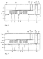
- a structured layer 5 is arranged in the substrate 3, in which Functional structures 7 and support structures are formed.
- the Functional structures 7 are in the concrete Embodiment in the structured layer 5 as interlocking combs or interdigital structures with fixed and deflectable electrodes.
- the Support structures are provided by a frame 15, which the Surrounds functional structures 7, and a support element 6 is formed, that within the frame 15 in the area of Functional structures 7 is arranged and for mechanical Stability of the layer system contributes.
- a support element 6 shown between the two shown Functional structures 7 is arranged.
- a single support element 6 or several spaced apart support elements in the Area of the functional structures can be provided.
- the support element or the Support elements arranged so that the freedom of movement Functional structures 7 is not affected.
- An approximately flat cap 1 is over a Connection layer 2 with the support structures 6 and 15 of the structured layer 5 connected and covers the Functional structures 7.
- the support structures 6 and 15 are in the Compared to the functional structures 7 increased (see FIG. 3) and protrude beyond the functional structures 7 preferably by about 4 - 10 ⁇ m, so that cavities 7a in the Form area of the functional structures 7 or between the Open functional structures 7 and cap 1.
- the underside of the cap i.e. on the side of the cap that corresponds to the functional structures 7 facing a deepening in the area of Functional structures are provided so that the recess the cavity or cavities 7a above the functional structures 7 forms in whole or in part (not shown).
- connection layer 2 is in the area of Functional structures 7 removed, so that the clamping height H of the cavities 7a enlarged accordingly.
- the clamping height H of the cavities 7a is always such that a destructive deflection of the functional structures 7 in vertical direction, i.e. the z direction.
- the Total span of the cavities 7a lies in the lateral direction preferably between about 100 and 500 microns. Spans up to however, several mm are also possible.
- connection surfaces 4 are associated with the cap 1 ends 6a and 15a of the Support element 6 and the frame 15 .
- the Connection surfaces 4 have a width of less than 150 microns and a high surface quality or a low one Surface roughness, which is preferably about 40 nm or less is.
- the support element 6 and the frame 15 are with their second ends 6b and 15b connected to the substrate 3.
- Conductor tracks 13 are provided which are used for external contacting of the Functional structures 7 serve.
- the conductor tracks 13 are in the near Area placed below the functional structures 7 and run through bushings 6c and 15c of the support structures 6 and 15, with two sacrificial layers 16 and 17 (see FIG. 2) the conductor tracks 13 opposite the support structures 6 and 15 isolate.
- connection area 14 For external contacting of the functional structures 7 is also in the substrate 3, a connection area 14, largely directly in addition to the functional structures 7, which is formed on the structured layer 5 facing top 3b of the Substrate 3 in direct contact with a contact tongue 18 the conductor tracks 13 is.
- the connection area 14 is completely surrounded by trenches 14a which form an isolation frame form.
- the trenches 14a extend from the Bottom of the substrate to the top of the substrate, so that the thereby formed connection area 14 with respect to the substrate 3 is electrically insulated.
- the trenches 14a preferably have high aspect ratio, i.e. a great depth and a shallow one lateral dimension, on.
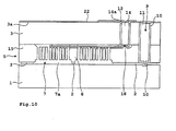
- connection area 14 On the connection area 14 is on its rear side 3a facing away from the structured layer 5 of the substrate 3, a metallization 12 applied preferably a conductor track and a contact pad for attachment of bond wires through which an external electrical Connection to the functional structures 7 is established.
- the Metallization 12 is on the rear side 3a of the substrate 3 through a dielectric layer 22 opposite the substrate 3 isolated.
- the metallization 12 and thus the conductor track and that Contact pads preferably extend from the connection area 14 horizontally in the direction of the functional structures 7, whereby the wafer or necessary for the production of the component Substrate area can be reduced in a cost-saving manner can.
- connection area 14 for external contacting the Functional structures 7 largely in the center under the support element 6 manufactured. This leads to a space saving for the manufacture of the component required wafer or Substrate area, which with a cost-saving reduction in Volume of the component goes hand in hand. The packing density will elevated.
- the structured one Layer 5 and the cap 1 provided a conductive connection 8, to potential differences between the substrate 3 and to avoid the cap 1.
- the conductive connection 8 comprises a Blind hole or a passage 9, which is outside the Area of the conductor tracks 13 through the substrate 3, the frame 15 and extends into part of the cap 1.
- a Conductor layer 10, in particular a metal layer, on the Bottom and the wall surfaces 9a of the passage 9 is applied, connects the substrate 3, the structured layer 5 and the Cap 1.
- a filler layer 11 closes the passage 9 the back 3a of the substrate 3 and paves the topography on.
- FIG. 2 shows the layer structure of the component as it appears before the structured layer 5 is structured in depth.
- a first sacrificial layer 16 is applied, which can consist, for example, of one or more SiO 2 layers.
- Conductor tracks 13 are deposited on the first sacrificial layer 16, which are made of polycrystalline silicon, which is doped sufficiently for the greatest possible conductivity.
- the first sacrificial layer 16 is pre-structured before the application of the conductor tracks 13, a contact opening for the correspondingly shaped contact tongue 18 for each of the conductor tracks 13 being etched into the first sacrificial layer 16.
- connection tongues 18 directly adjoins the substrate 3 and is in direct connection with the connection region 14 which is later formed in the substrate 3.
- the described production of the connection regions and their respective external contacting takes place in the same way as the production and external ones Contacting the explicitly shown connection area 14.
- a second sacrificial layer 17 is deposited on the conductor tracks 13 and, like the first sacrificial layer 16, serves as an insulation layer and consists of SiO 2 .
- Preferred deposition processes for producing the second sacrificial layer 17 are CVD processes, such as using tetraethyl orthosilicate (TEOS).
- TEOS tetraethyl orthosilicate
- a thin starting poly-silicon layer 5a ie a polycrystalline silicon layer with the function of a seed or nucleation layer, is then deposited on the second sacrificial layer 17.
- An epitaxial process is used to apply a polycrystalline silicon layer, which is the structured layer 5 formed below, to the start poly-Si layer 5a, the start poly-Si layer being absorbed in the upper polycrystalline layer.
- the surface of the upper polycrystalline layer 5 is planarized in a further process step. This is done by means of a chemical-mechanical polishing process (CMP), with which a surface roughness is achieved in which the surfaces can be bonded well to the connecting layer 2 by applying a differential voltage or can be anodically bonded.
- CMP chemical-mechanical polishing process
- the surface roughness is preferably approximately 2 nm to approximately 50 nm.
- the sacrificial layers 16 and 17 are advantageously before Deposition of the start poly-Si layer 5a structured. there the first and second sacrificial layers 16 and 17 in Areas 16a in which in a later process step Support structures 6 and 15 are formed, partially or completely removed, so that the support structures 6 and 15 are directly connected to the substrate. In the second Sacrificial layer 17 becomes contact openings 17a for contacting the functional structures 7 are formed with the conductor tracks 13.
- an oxide mask 20 is applied to the connecting surfaces 4 using a CVD method, the connecting surfaces 4 being located in the region of the support structures 6 and 15 formed later. Due to its good Si / SiO 2 selectivity, the oxide mask 20 deposited from the gas phase serves as a passivation layer and ensures that the connecting surfaces 4 are not attacked in a later plasma etching step or chemical mechanical polishing process (CMP). With a dry etching method or with a further CMP step, planar recesses 21 are etched or formed in areas 7 of the structured layer 5, in which the functional structures 7 are later structured. The oxide mask 20 is then removed.
- CMP chemical mechanical polishing process
- the Support structures 6 and 15 with respect to their height (and possibly in with respect to their width) compared to the functional structures 7 pre-structured by the structured layer 5 in the Areas of the functional structures 7 around a defined Amount is thinned.
- connection layer with a corresponding one larger thickness dimension used (case not shown).
- the functional structures 7 and the support element 6 with a deep structuring process (trench etching) structured.
- the second sacrificial layer 17 and partly also the first sacrificial layer 16 are below the Functional structures 7 with a gas phase etching process removed, so that deflectable structures arise.
- the hermetically sealed Capping the component or sensor layer system as in Fig. 5 is shown.
- the cap 1 made of single crystal silicon exists, with the connecting surfaces 4 of the support structures 6 and 15 chemically bonded via the connection layer 2.
- the connecting layer 2 consists of an approximately 10-50 ⁇ m thick silicate glass, which is preferably made by chemical and / or mechanical treatment from a thicker, e.g. B. 500 microns thick, silicate glass wafer is produced.
- the silicate glass has a defined concentration of mono- or polyvalent cations, such as Na + or B 3+ , and a corresponding concentration of weakly bound oxygen atoms.
- Particularly suitable silicates are alkali and borosilicates.
- the cap 1 on the connecting layer 2nd facing side chemically-mechanically polished.
- the Surface roughness is typically after the CMP step below 2 nm.
- the cap 1 with the connecting layer 2 by applying a voltage difference between the cap and the connection layer 2, typically about - 150 to - 1000 V, the cap 1 being connected to ground, connected flat.
- connection step Temperature of about 350 - 450 ° C on the connection layer 2 act on the mobility of the metal or boron cations to increase.
- the reduced cation concentration can for example by a subsequent exposure to temperature be balanced.
- Supply voltage after connecting the cap 1 with the Connection layer 2 reversed to the resulting, reduced Concentration of the cations at the interface of the Compensate connection layer 2 to cap 1.
- connection layer 2 in the form of a Melt can be applied to the cap 1, the Melting or softening temperature depending on the type of silicate glass used in a range of about 600-800 ° C.
- the connection layer 2 processed as described below.
- connection layer 2 After connection of the cap 1 to the connection layer 2 the connection layer 2 according to the above first or second alternatives on the connecting surfaces 4 facing side roughly ground or thinned mechanically and then polished with a CMP step to get a good one Joint connection with the connecting surfaces 4 of the structured To produce layer 5.
- connection layer 2 has one Thickness of about 10 - 50 ⁇ m and a surface roughness of 2 nm or less.
- connection layer by sputtering silicate glass, such as especially electron beam sputtering. before the cap is thermally oxidized, resulting in an approx. 1 to 2 ⁇ m thick silicon oxide layer is formed on which the Connection layer is deposited by sputtering.
- the Silicon oxide layer improves the electrical Dielectric strength during anodic bonding.
- preferred Layer thicknesses for a sputter formed Connection layer are in the range from about 300nm to 2 ⁇ m.
- connection layer 2 is all three of the above Alternatives in the area of functional structures 7 removed or structured to the clamping height H of the cavities 7a enlarge.
- connection layer 2 is also in the area of the later formed passage 9 of the conductive connection 8 removed.
- the connection surfaces 4 and the connection layer 2 are adjusted to each other and by the applied supply voltage and / or under Effect of temperature chemically combined (anodic bonding).
- a cap is attached to the cap in relation to the bonding Cap 1 with the connection layer 2 lower voltage to the Cap applied to excessive deflection of the To prevent functional structures 7 due to the bond voltage.
- this can be - 100 V on cap 1, where the substrate 3 is grounded.
- capping is preferably a gas with a pressure between 1 mbar and 1 bar enclosed in the cavities 7a, wherein about the pressure damping the movement of the Functional structures 7 is set.
- a closable opening Liquid is introduced into the cavities 7a, whereby whose viscosity determines the degree of damping, or a Gas or another gas.
- the basic doping of the n-doped substrate 3 is typically greater than approximately 5 * 10 15 / cm 3 and the ohmic resistance is less than approximately 1 Ohm * cm (low resistance).
- the doping of the n-doped functional layer 5 is approximately 10 17 / cm 3 to 10 19 / cm 3 , which enables a low-resistance external contact with the functional structures 7.
- connection between the cap 1 and the Connection layer 2 on the one hand and between the Connection layer 2 and the connection surfaces 4 and the structured layer 5 on the other hand is a hermetically sealed connection between the cap 1 and the Connection layer 2 on the one hand and between the Connection layer 2 and the connection surfaces 4 and the structured layer 5 on the other hand.
- relatively small connecting surfaces 4 are required.
- the width of the connection areas is only about 30 to 150 ⁇ m.
- the rear 3a is mechanically ground back Substrate 3 (see. Fig. 6). This is preferably done in several steps: First, the back 3a of the substrate 3 with a large abrasive diamond grinding wheel ground and then with a diamond grinding wheel small grain size with correspondingly less removal abraded. Alternatively, the grinding can also be done in one single step. The surface roughness is after the fine sanding about 0.1 - 1 ⁇ m and the depth of Crystal dislocations amount to about 3 - 5 ⁇ m.
- the crystal dislocations are removed using a CMP process and further improves the surface quality.
- the deduction is about 10 ⁇ m.
- using so-called Spin etching removed the crystal dislocations in substrate 3 become.
- the removal is typically 5 to 10 ⁇ m.
- the deduction is then still typically 3 ⁇ m.
- the residual thickness K of the substrate 3 is selected so that the static strength of the layer system is guaranteed, the support elements 6 significantly increase the static strength improve. Especially with small spans can be Support elements are dispensed with. Typically that is Residual thickness K of the substrate 3 is approximately 80-150 ⁇ m.
- the conductive layer 10 is on the Floor surface and the wall surfaces 9a of the passage 9 or Blind hole applied by being on the back 3a of the Substrate 3 is deposited.
- a filler layer 11 which closes the passage 9 and the surface topography flattens.
- the filling layer 11 is preferably a silicon oxide layer. This is preferred by a so-called spin-on method or by introducing and Curing a filler containing silicon oxide, manufactured.
- the filling layer 11 is etched back. Then the Conductive layer 10 on the rear side 3a of the substrate 3 removed by wet chemical means. It is important to ensure that the Conductive layer 10 in the region of the trenches 14a has been completely removed is not overestimated in the area of the passage 9 so that no undesired topographies form.
- the dielectric layer 22 becomes with a CVD process on the rear side 3a of the substrate 3 applied.
- the dielectric layer 22 serves as Insulation layer and insulates the one subsequently applied Metallization 12 relative to the substrate 3.
- the metallization 12 is shown on the dielectric layer 22 and via the contact opening 23 the connection area 14 applied and preferably becomes a trace or a connection wet-chemically structured, the connection pad preferably in Extends towards the center of the component. This leaves needed to manufacture the component Reduce substrate area and its volume to save costs.
- sensor or actuator structures together with an electronic evaluation circuit (not shown) in the cap 1 and / or in the to integrate structured layer 5.
- the component described above is characterized a compact and robust design that integrates a variety of functional structures and at the same time one sufficient freedom of movement of the functional structures allowed.
- the process described above enables production a variety of components that are hermetically sealed Require capping.
- the one for the capping or the Connection areas required is kept to a minimum reduced.
Landscapes
- Engineering & Computer Science (AREA)
- Microelectronics & Electronic Packaging (AREA)
- Computer Hardware Design (AREA)
- Manufacturing & Machinery (AREA)
- Micromachines (AREA)
- Pressure Sensors (AREA)
- Laminated Bodies (AREA)
Priority Applications (2)
| Application Number | Priority Date | Filing Date | Title |
|---|---|---|---|
| EP06110978A EP1671924B1 (fr) | 2001-02-03 | 2001-10-27 | Dispositif micromécanique et procédé de fabrication d'un dispositif micro mécanique |
| EP06110976A EP1671923B1 (fr) | 2001-02-03 | 2001-10-27 | Dispositif micromécanique et procédé de fabrication d'un dispositif micromécanique |
Applications Claiming Priority (2)
| Application Number | Priority Date | Filing Date | Title |
|---|---|---|---|
| DE10104868A DE10104868A1 (de) | 2001-02-03 | 2001-02-03 | Mikromechanisches Bauelement sowie ein Verfahren zur Herstellung eines mikromechanischen Bauelements |
| DE10104868 | 2001-02-03 |
Related Child Applications (2)
| Application Number | Title | Priority Date | Filing Date |
|---|---|---|---|
| EP06110976A Division EP1671923B1 (fr) | 2001-02-03 | 2001-10-27 | Dispositif micromécanique et procédé de fabrication d'un dispositif micromécanique |
| EP06110978A Division EP1671924B1 (fr) | 2001-02-03 | 2001-10-27 | Dispositif micromécanique et procédé de fabrication d'un dispositif micro mécanique |
Publications (3)
| Publication Number | Publication Date |
|---|---|
| EP1228998A2 true EP1228998A2 (fr) | 2002-08-07 |
| EP1228998A3 EP1228998A3 (fr) | 2004-06-16 |
| EP1228998B1 EP1228998B1 (fr) | 2006-06-14 |
Family
ID=7672725
Family Applications (3)
| Application Number | Title | Priority Date | Filing Date |
|---|---|---|---|
| EP06110976A Expired - Lifetime EP1671923B1 (fr) | 2001-02-03 | 2001-10-27 | Dispositif micromécanique et procédé de fabrication d'un dispositif micromécanique |
| EP06110978A Expired - Lifetime EP1671924B1 (fr) | 2001-02-03 | 2001-10-27 | Dispositif micromécanique et procédé de fabrication d'un dispositif micro mécanique |
| EP01125720A Expired - Lifetime EP1228998B1 (fr) | 2001-02-03 | 2001-10-27 | Dispositif microméchanique et procédé de fabrication d'un dispositif microméchanique |
Family Applications Before (2)
| Application Number | Title | Priority Date | Filing Date |
|---|---|---|---|
| EP06110976A Expired - Lifetime EP1671923B1 (fr) | 2001-02-03 | 2001-10-27 | Dispositif micromécanique et procédé de fabrication d'un dispositif micromécanique |
| EP06110978A Expired - Lifetime EP1671924B1 (fr) | 2001-02-03 | 2001-10-27 | Dispositif micromécanique et procédé de fabrication d'un dispositif micro mécanique |
Country Status (4)
| Country | Link |
|---|---|
| US (2) | US6876048B2 (fr) |
| EP (3) | EP1671923B1 (fr) |
| JP (2) | JP4243064B2 (fr) |
| DE (4) | DE10104868A1 (fr) |
Cited By (8)
| Publication number | Priority date | Publication date | Assignee | Title |
|---|---|---|---|---|
| WO2004031070A1 (fr) * | 2002-10-03 | 2004-04-15 | Sharp Kabushiki Kaisha | Dispositif micro-mobile |
| WO2004035461A3 (fr) * | 2002-10-18 | 2004-08-05 | Univ Michigan | Procedes de fabrication et dispositifs a systemes mecaniques microelectriques ou a micro-usinage emballe hermetiquement ou sous vide formes a partir des procedes de fabrication et possedant des trous d'interconnexion sensiblement verticaux |
| EP1394841A3 (fr) * | 2002-08-27 | 2005-03-23 | Hahn-Schickard-Gesellschaft Für Angewandte Forschung E.V. | Procédé de collage sélectif des substrats |
| FR2860779A1 (fr) * | 2003-10-10 | 2005-04-15 | Bosch Gmbh Robert | Procede de fabrication d'un capteur micromecanique et capteur obtenu |
| WO2007068590A1 (fr) * | 2005-12-15 | 2007-06-21 | Robert Bosch Gmbh | Composant micromecanique et procede de fabrication dudit composant |
| WO2007074017A1 (fr) * | 2005-12-27 | 2007-07-05 | Robert Bosch Gmbh | Élément de construction micromécanique doté d'une couverture |
| EP1580161B1 (fr) * | 2004-03-24 | 2008-04-09 | Hewlett-Packard Development Company, L.P. | Procédé de formation d'une chambre dans un dispositif électronique et dispositif ainsi formé |
| CN103373697A (zh) * | 2012-04-25 | 2013-10-30 | 罗伯特·博世有限公司 | 混合集成的部件和用于其制造的方法 |
Families Citing this family (66)
| Publication number | Priority date | Publication date | Assignee | Title |
|---|---|---|---|---|
| DE10047189C1 (de) * | 2000-09-23 | 2002-02-21 | Bosch Gmbh Robert | Verfahren zur Insassenklassifikation mit einer Sitzmatte im Fahrzeugsitz |
| DE10104868A1 (de) * | 2001-02-03 | 2002-08-22 | Bosch Gmbh Robert | Mikromechanisches Bauelement sowie ein Verfahren zur Herstellung eines mikromechanischen Bauelements |
| WO2003087459A1 (fr) * | 2002-04-10 | 2003-10-23 | Fisher & Paykel Appliances Limited | Appareil de blanchissage |
| DE10231729B4 (de) * | 2002-07-13 | 2011-08-11 | Robert Bosch GmbH, 70469 | Bauelement mit einer oberflächenmikromechanischen Struktur |
| FR2856844B1 (fr) * | 2003-06-24 | 2006-02-17 | Commissariat Energie Atomique | Circuit integre sur puce de hautes performances |
| US6952041B2 (en) * | 2003-07-25 | 2005-10-04 | Robert Bosch Gmbh | Anchors for microelectromechanical systems having an SOI substrate, and method of fabricating same |
| FR2861497B1 (fr) | 2003-10-28 | 2006-02-10 | Soitec Silicon On Insulator | Procede de transfert catastrophique d'une couche fine apres co-implantation |
| DE10356885B4 (de) * | 2003-12-03 | 2005-11-03 | Schott Ag | Verfahren zum Gehäusen von Bauelementen und gehäustes Bauelement |
| GB0330010D0 (en) * | 2003-12-24 | 2004-01-28 | Cavendish Kinetics Ltd | Method for containing a device and a corresponding device |
| EP1738411A4 (fr) * | 2004-04-22 | 2012-06-27 | Panasonic Corp | Dispositif de capteur, système de capteur et procédés de fabrication de ceux-ci |
| DE102004027501A1 (de) * | 2004-06-04 | 2005-12-22 | Robert Bosch Gmbh | Mikromechanisches Bauelement mit mehreren Kavernen und Herstellungsverfahren |
| JP2006043813A (ja) * | 2004-08-04 | 2006-02-16 | Denso Corp | 保護膜付きマイクロシステム構造体及びその製造方法 |
| US7416984B2 (en) * | 2004-08-09 | 2008-08-26 | Analog Devices, Inc. | Method of producing a MEMS device |
| US7816745B2 (en) * | 2005-02-25 | 2010-10-19 | Medtronic, Inc. | Wafer level hermetically sealed MEMS device |
| DE102005040789B4 (de) | 2005-08-29 | 2014-12-24 | Robert Bosch Gmbh | Herstellungsverfahren für ein Mikromechanisches Bauelement mit anodisch gebondeter Kappe |
| FR2891281B1 (fr) | 2005-09-28 | 2007-12-28 | Commissariat Energie Atomique | Procede de fabrication d'un element en couches minces. |
| DE102005053682A1 (de) * | 2005-11-10 | 2007-05-16 | Bosch Gmbh Robert | Sensor, Sensorbauelement und Verfahren zur Herstellung eines Sensors |
| DE102005061312A1 (de) | 2005-12-20 | 2007-08-16 | Otto Bock Healthcare Ip Gmbh & Co. Kg | Handprothese |
| DE102005061313A1 (de) | 2005-12-20 | 2007-08-16 | Otto Bock Healthcare Ip Gmbh & Co. Kg | Handprothese |
| DE102006010484A1 (de) | 2006-03-07 | 2007-09-13 | Robert Bosch Gmbh | Bewegungssensor |
| FR2898597B1 (fr) * | 2006-03-16 | 2008-09-19 | Commissariat Energie Atomique | Encapsulation dans une cavite hermetique d'un compose microelectronique, notamment d'un mems |
| US8323570B2 (en) | 2006-03-21 | 2012-12-04 | Koninklijke Philips Electronics N.V. | Microelectronic sensor device with sensor array |
| DE102006023701A1 (de) * | 2006-05-19 | 2007-11-22 | Robert Bosch Gmbh | Mikromechanisches Bauelement und Verfahren zur Herstellung eines mikromechanischen Bauelements |
| JP5545281B2 (ja) * | 2006-06-13 | 2014-07-09 | 株式会社デンソー | 力学量センサ |
| DE102006031772A1 (de) | 2006-07-10 | 2008-01-17 | Robert Bosch Gmbh | Verfahren zur Herstellung eines Sensorelements sowie Sensorelement |
| JP2008256495A (ja) * | 2007-04-04 | 2008-10-23 | Denso Corp | センサ装置 |
| DE102007019647A1 (de) * | 2007-04-26 | 2008-10-30 | Robert Bosch Gmbh | Verfahren zur Herstellung eines mikromechanischen Bauelements mit Auffüllschicht und Maskenschicht |
| DE102007019639A1 (de) | 2007-04-26 | 2008-10-30 | Robert Bosch Gmbh | Mikromechanisches Bauelement und entsprechendes Herstellungsverfahren |
| JP2008304218A (ja) | 2007-06-05 | 2008-12-18 | Mitsubishi Electric Corp | 加速度センサおよびその製造方法 |
| US7932179B2 (en) * | 2007-07-27 | 2011-04-26 | Micron Technology, Inc. | Method for fabricating semiconductor device having backside redistribution layers |
| JP2009053034A (ja) * | 2007-08-27 | 2009-03-12 | Mitsumi Electric Co Ltd | 半導体圧力センサ及びその製造方法 |
| DE102007044806A1 (de) * | 2007-09-20 | 2009-04-02 | Robert Bosch Gmbh | Mikromechanisches Bauelement und Verfahren zur Herstellung eines mikromechanischen Bauelements |
| JP2009090429A (ja) * | 2007-10-10 | 2009-04-30 | Disco Abrasive Syst Ltd | マイクロマシンデバイスの加工方法 |
| DE102007060785B4 (de) * | 2007-12-17 | 2011-12-15 | Fraunhofer-Gesellschaft zur Förderung der angewandten Forschung e.V. | Verfahren zur Herstellung eines (Vielfach-) Bauelements auf Basis ultraplanarer Metallstrukturen |
| US7989262B2 (en) | 2008-02-22 | 2011-08-02 | Cavendish Kinetics, Ltd. | Method of sealing a cavity |
| US7993950B2 (en) * | 2008-04-30 | 2011-08-09 | Cavendish Kinetics, Ltd. | System and method of encapsulation |
| JP4766143B2 (ja) | 2008-09-15 | 2011-09-07 | 株式会社デンソー | 半導体装置およびその製造方法 |
| JP5314979B2 (ja) * | 2008-09-22 | 2013-10-16 | アルプス電気株式会社 | Memsセンサ |
| WO2010032819A1 (fr) * | 2008-09-22 | 2010-03-25 | アルプス電気株式会社 | Capteur mems |
| JP5468242B2 (ja) * | 2008-11-21 | 2014-04-09 | 株式会社東芝 | Memsパッケージおよびmemsパッケージの製造方法 |
| US8089144B2 (en) | 2008-12-17 | 2012-01-03 | Denso Corporation | Semiconductor device and method for manufacturing the same |
| JP4858547B2 (ja) * | 2009-01-09 | 2012-01-18 | 株式会社デンソー | 半導体装置およびその製造方法 |
| JPWO2010104064A1 (ja) * | 2009-03-13 | 2012-09-13 | アルプス電気株式会社 | Memsセンサ |
| JP4793496B2 (ja) * | 2009-04-06 | 2011-10-12 | 株式会社デンソー | 半導体装置およびその製造方法 |
| FR2947098A1 (fr) | 2009-06-18 | 2010-12-24 | Commissariat Energie Atomique | Procede de transfert d'une couche mince sur un substrat cible ayant un coefficient de dilatation thermique different de celui de la couche mince |
| DE102010029504B4 (de) | 2010-05-31 | 2014-02-27 | Robert Bosch Gmbh | Bauelement mit einer Durchkontaktierung und Verfahren zu dessen Herstellung |
| CN102398886B (zh) * | 2010-09-15 | 2014-07-23 | 矽品精密工业股份有限公司 | 具微机电元件的封装结构及其制法 |
| FR2977884B1 (fr) * | 2011-07-12 | 2016-01-29 | Commissariat Energie Atomique | Procede de realisation d'une structure a membrane suspendue et a electrode enterree |
| FR2977885A1 (fr) | 2011-07-12 | 2013-01-18 | Commissariat Energie Atomique | Procede de realisation d'une structure a electrode enterree par report direct et structure ainsi obtenue |
| CN102320558B (zh) * | 2011-09-13 | 2014-03-26 | 上海先进半导体制造股份有限公司 | 全硅基微流体器件的腔体的制造方法 |
| US8633088B2 (en) * | 2012-04-30 | 2014-01-21 | Freescale Semiconductor, Inc. | Glass frit wafer bond protective structure |
| JP5950226B2 (ja) * | 2012-06-07 | 2016-07-13 | ローム株式会社 | 静電容量型圧力センサおよびその製造方法、圧力センサパッケージ |
| DE102012219616B4 (de) * | 2012-10-26 | 2021-05-20 | Robert Bosch Gmbh | Mikromechanisches Bauelement mit Bondverbindung |
| JP6237440B2 (ja) * | 2014-04-23 | 2017-11-29 | 株式会社デンソー | 物理量センサおよびその製造方法 |
| DE102014223926A1 (de) | 2014-11-25 | 2016-05-25 | Robert Bosch Gmbh | Verfahren zum Herstellen eines MEMS-Bauelements mit zwei miteinander verbundenen Substraten und entsprechendes MEMS-Bauelement |
| US10315915B2 (en) * | 2015-07-02 | 2019-06-11 | Kionix, Inc. | Electronic systems with through-substrate interconnects and MEMS device |
| US20170021380A1 (en) * | 2015-07-21 | 2017-01-26 | Tangitek, Llc | Electromagnetic energy absorbing three dimensional flocked carbon fiber composite materials |
| JP2017053742A (ja) * | 2015-09-10 | 2017-03-16 | セイコーエプソン株式会社 | 電子デバイスの製造方法、電子デバイス、電子機器、および移動体 |
| KR101988469B1 (ko) * | 2017-07-26 | 2019-06-13 | 주식회사 신성씨앤티 | 멤스 센서 및 그 제조 방법 |
| DE102017223372A1 (de) * | 2017-12-20 | 2019-06-27 | Robert Bosch Gmbh | Laserbondverfahren und mikromechanische Vorrichtung mit Laserbondverbindung |
| DE102018100173A1 (de) | 2018-01-05 | 2019-07-11 | Otto Bock Healthcare Products Gmbh | Greifeinrichtung |
| DE102018210810B3 (de) | 2018-06-29 | 2019-08-08 | Fraunhofer-Gesellschaft zur Förderung der angewandten Forschung e.V. | Mikromechanisches bauteil und verfahren zur herstellung |
| DE102018222804B4 (de) | 2018-12-21 | 2022-03-24 | Robert Bosch Gmbh | Mikromechanische Vorrichtung und Verfahren zur Herstellung einer mikromechanischen Vorrichtung |
| CN110040682B (zh) * | 2019-04-19 | 2021-06-18 | 中国科学院上海微系统与信息技术研究所 | 高灵敏度加速度传感器结构的制备方法 |
| WO2024133144A2 (fr) | 2022-12-19 | 2024-06-27 | Otto Bock Healthcare Products Gmbh | Main prothétique |
| DE102022133976A1 (de) | 2022-12-19 | 2024-06-20 | Otto Bock Healthcare Products Gmbh | Prothesenhand |
Family Cites Families (28)
| Publication number | Priority date | Publication date | Assignee | Title |
|---|---|---|---|---|
| US4773972A (en) * | 1986-10-30 | 1988-09-27 | Ford Motor Company | Method of making silicon capacitive pressure sensor with glass layer between silicon wafers |
| US5343064A (en) * | 1988-03-18 | 1994-08-30 | Spangler Leland J | Fully integrated single-crystal silicon-on-insulator process, sensors and circuits |
| US5164338A (en) * | 1988-04-28 | 1992-11-17 | U.S. Philips Corporation | Method of manufacturing a polycrystalline semiconductor resistance layer of silicon on a silicon body and silicon pressure sensor having such a resistance layer |
| JPH0623782B2 (ja) * | 1988-11-15 | 1994-03-30 | 株式会社日立製作所 | 静電容量式加速度センサ及び半導体圧力センサ |
| DE3914015C2 (de) * | 1989-04-25 | 1998-03-19 | Siemens Ag | Verfahren zum Verbinden von Silizium-Einkristall-Bauteilen |
| FI84096B (fi) * | 1990-01-31 | 1991-06-28 | Halton Oy | Undertakskonstruktion och foerfarande foer att bringa luften att stroemma i samband med undertakskonstruktionen. |
| DE4006108A1 (de) * | 1990-02-27 | 1991-08-29 | Bosch Gmbh Robert | Verfahren zum aufbau von mikromechanischen bauelementen in dickschichttechnik |
| FR2687778B1 (fr) * | 1992-02-20 | 1994-05-20 | Sextant Avionique | Micro-capteur capacitif a capacite parasite reduite et procede de fabrication. |
| TW276357B (fr) | 1993-03-22 | 1996-05-21 | Motorola Inc | |
| JP3114459B2 (ja) * | 1993-09-24 | 2000-12-04 | 株式会社村田製作所 | 圧電素子の製造方法 |
| JP3173256B2 (ja) * | 1993-11-08 | 2001-06-04 | 日産自動車株式会社 | 半導体加速度センサとその製造方法 |
| JP3198779B2 (ja) * | 1994-03-04 | 2001-08-13 | 株式会社デンソー | 半導体圧力検出器の製造方法 |
| US5511428A (en) * | 1994-06-10 | 1996-04-30 | Massachusetts Institute Of Technology | Backside contact of sensor microstructures |
| JP3319912B2 (ja) * | 1995-06-29 | 2002-09-03 | 株式会社デンソー | 半導体センサ用台座およびその加工方法 |
| DE19537814B4 (de) * | 1995-10-11 | 2009-11-19 | Robert Bosch Gmbh | Sensor und Verfahren zur Herstellung eines Sensors |
| JPH09222372A (ja) * | 1996-02-19 | 1997-08-26 | Mitsubishi Electric Corp | 半導体式センサ |
| DE19643893A1 (de) | 1996-10-30 | 1998-05-07 | Siemens Ag | Ultraschallwandler in Oberflächen-Mikromechanik |
| DE69823904T2 (de) * | 1997-03-20 | 2005-06-16 | F. Hoffmann-La Roche Ag | Mikromechanische Pipettiervorrichtung |
| FR2763745B1 (fr) * | 1997-05-23 | 1999-08-27 | Sextant Avionique | Procede de fabrication d'un micro-capteur en silicium usine |
| JPH1151967A (ja) * | 1997-08-08 | 1999-02-26 | Mitsubishi Electric Corp | 多軸加速度センサ及びその製造方法 |
| DE19830158C2 (de) * | 1997-09-30 | 2001-05-10 | Tyco Electronics Logistics Ag | Zwischenträgersubstrat mit hoher Verdrahtungsdichte für elektronische Bauelemente |
| WO2004090556A1 (fr) * | 1997-11-11 | 2004-10-21 | Makoto Ishida | Capteur d'acceleration integre en silicium |
| US6232150B1 (en) * | 1998-12-03 | 2001-05-15 | The Regents Of The University Of Michigan | Process for making microstructures and microstructures made thereby |
| US6225692B1 (en) * | 1999-06-03 | 2001-05-01 | Cts Corporation | Flip chip package for micromachined semiconductors |
| DE19931773C1 (de) * | 1999-07-08 | 2000-11-30 | Daimler Chrysler Ag | Mikromechanisches Bauelement mit Kontaktdurchführungen, sowie Verfahren zur Herstellung eines mikromechanischen Bauelements |
| JP2001038699A (ja) * | 1999-07-26 | 2001-02-13 | Sony Corp | 接合基板素子および接合基板素子製造方法 |
| DE10055081A1 (de) * | 2000-11-07 | 2002-05-16 | Bosch Gmbh Robert | Mikrostrukturbauelement |
| DE10104868A1 (de) * | 2001-02-03 | 2002-08-22 | Bosch Gmbh Robert | Mikromechanisches Bauelement sowie ein Verfahren zur Herstellung eines mikromechanischen Bauelements |
-
2001
- 2001-02-03 DE DE10104868A patent/DE10104868A1/de not_active Ceased
- 2001-10-27 DE DE50115279T patent/DE50115279D1/de not_active Expired - Lifetime
- 2001-10-27 DE DE50113572T patent/DE50113572D1/de not_active Expired - Lifetime
- 2001-10-27 EP EP06110976A patent/EP1671923B1/fr not_active Expired - Lifetime
- 2001-10-27 EP EP06110978A patent/EP1671924B1/fr not_active Expired - Lifetime
- 2001-10-27 DE DE50110147T patent/DE50110147D1/de not_active Expired - Lifetime
- 2001-10-27 EP EP01125720A patent/EP1228998B1/fr not_active Expired - Lifetime
-
2002
- 2002-01-31 JP JP2002024155A patent/JP4243064B2/ja not_active Expired - Fee Related
- 2002-02-04 US US10/066,851 patent/US6876048B2/en not_active Expired - Fee Related
-
2004
- 2004-04-21 US US10/829,872 patent/US7153718B2/en not_active Expired - Fee Related
-
2008
- 2008-05-07 JP JP2008121530A patent/JP2008183717A/ja active Pending
Cited By (12)
| Publication number | Priority date | Publication date | Assignee | Title |
|---|---|---|---|---|
| EP1394841A3 (fr) * | 2002-08-27 | 2005-03-23 | Hahn-Schickard-Gesellschaft Für Angewandte Forschung E.V. | Procédé de collage sélectif des substrats |
| WO2004031070A1 (fr) * | 2002-10-03 | 2004-04-15 | Sharp Kabushiki Kaisha | Dispositif micro-mobile |
| WO2004035461A3 (fr) * | 2002-10-18 | 2004-08-05 | Univ Michigan | Procedes de fabrication et dispositifs a systemes mecaniques microelectriques ou a micro-usinage emballe hermetiquement ou sous vide formes a partir des procedes de fabrication et possedant des trous d'interconnexion sensiblement verticaux |
| US7098117B2 (en) | 2002-10-18 | 2006-08-29 | The Regents Of The University Of Michigan | Method of fabricating a package with substantially vertical feedthroughs for micromachined or MEMS devices |
| FR2860779A1 (fr) * | 2003-10-10 | 2005-04-15 | Bosch Gmbh Robert | Procede de fabrication d'un capteur micromecanique et capteur obtenu |
| US7213465B2 (en) | 2003-10-10 | 2007-05-08 | Robert Bosch Gmbh | Micromechanical sensor |
| EP1580161B1 (fr) * | 2004-03-24 | 2008-04-09 | Hewlett-Packard Development Company, L.P. | Procédé de formation d'une chambre dans un dispositif électronique et dispositif ainsi formé |
| WO2007068590A1 (fr) * | 2005-12-15 | 2007-06-21 | Robert Bosch Gmbh | Composant micromecanique et procede de fabrication dudit composant |
| US7919346B2 (en) | 2005-12-15 | 2011-04-05 | Robert Bosch Gmbh | Micromechanical component and manufacturing method |
| WO2007074017A1 (fr) * | 2005-12-27 | 2007-07-05 | Robert Bosch Gmbh | Élément de construction micromécanique doté d'une couverture |
| CN103373697A (zh) * | 2012-04-25 | 2013-10-30 | 罗伯特·博世有限公司 | 混合集成的部件和用于其制造的方法 |
| CN103373697B (zh) * | 2012-04-25 | 2017-04-12 | 罗伯特·博世有限公司 | 混合集成的部件和用于其制造的方法 |
Also Published As
| Publication number | Publication date |
|---|---|
| JP2008183717A (ja) | 2008-08-14 |
| DE50113572D1 (de) | 2008-03-20 |
| EP1671924B1 (fr) | 2009-12-23 |
| DE50110147D1 (de) | 2006-07-27 |
| EP1671923A3 (fr) | 2006-08-09 |
| JP2002273699A (ja) | 2002-09-25 |
| US7153718B2 (en) | 2006-12-26 |
| EP1228998A3 (fr) | 2004-06-16 |
| US20040195638A1 (en) | 2004-10-07 |
| EP1671924A2 (fr) | 2006-06-21 |
| US20030001221A1 (en) | 2003-01-02 |
| EP1671923B1 (fr) | 2008-02-06 |
| JP4243064B2 (ja) | 2009-03-25 |
| DE50115279D1 (de) | 2010-02-04 |
| US6876048B2 (en) | 2005-04-05 |
| EP1228998B1 (fr) | 2006-06-14 |
| DE10104868A1 (de) | 2002-08-22 |
| EP1671923A2 (fr) | 2006-06-21 |
| EP1671924A3 (fr) | 2006-08-16 |
Similar Documents
| Publication | Publication Date | Title |
|---|---|---|
| EP1671923B1 (fr) | Dispositif micromécanique et procédé de fabrication d'un dispositif micromécanique | |
| DE69305955T2 (de) | Beschleunigungssensor und seine herstellung | |
| DE69624645T2 (de) | Verfahren zum Herstellen einer monolithischen Halbleiteranordnung mit integrierten mikrogefertigten Oberflächenstrukturen | |
| DE10065013B4 (de) | Verfahren zum Herstellen eines mikromechanischen Bauelements | |
| DE102007060878B4 (de) | Mikromechanisches System | |
| DE102005015584B4 (de) | Verfahren zur Herstellung eines mikromechanischen Bauteils | |
| DE10006035A1 (de) | Verfahren zur Herstellung eines mikromechanischen Bauelements sowie ein nach dem Verfahren hergestelltes Bauelement | |
| DE102010029504B4 (de) | Bauelement mit einer Durchkontaktierung und Verfahren zu dessen Herstellung | |
| DE102005010944B4 (de) | Verfahren zur Herstellung eines Trägerscheibenkontaktes in integrierten Schaltungen mit Hochspannungsbauelementen auf der Basis der SOI-Technologie und integrierte Schaltungen mit entsprechenden Grabenstrukturen | |
| WO2001046066A2 (fr) | Capteur comportant au moins une structure micromecanique et procede de fabrication | |
| DE19503236A1 (de) | Sensor aus einem mehrschichtigen Substrat | |
| DE3900654A1 (de) | Drucksensoranordnung und verfahren zu deren herstellung | |
| DE10130379A1 (de) | Mikromechanischer Massenflusssensor und Verfahren zu dessen Herstellung | |
| DE19817311B4 (de) | Herstellungsverfahren für mikromechanisches Bauelement | |
| DE102012213313B4 (de) | Mikromechanische Struktur | |
| DE10350038A1 (de) | Verfahren zum anodischen Bonden von Wafern und Vorrichtung | |
| DE10324421B4 (de) | Halbleiterbauelement mit Metallisierungsfläche und Verfahren zur Herstellung desselben | |
| DE10029012C2 (de) | Mikrostruktur und Verfahren zu deren Herstellung | |
| EP2150488B1 (fr) | Procédé de fabrication d'un composant micromécanique comportant une couche de charge et une couche de masque | |
| DE10348908B4 (de) | Verfahren zur Herstellung eines Mikrosystems mit integrierter Schaltung und mikromechanischem Bauteil | |
| DE102010001021A1 (de) | Mikromechanisches Bauelement und entsprechendes Herstellungsverfahren | |
| DE102008040522A1 (de) | Verfahren zur Herstellung einer mikromechanischen Struktur und mikromechanische Struktur | |
| DE10231730A1 (de) | Mikrostrukturbauelement und Verfahren zu dessen Herstellung | |
| DE19964638B3 (de) | Verfahren zur Herstellung eines Sensors mit zumindest einer mikromechanischen Struktur | |
| DE102009046081B4 (de) | Eutektische Bondung von Dünnchips auf einem Trägersubstrat |
Legal Events
| Date | Code | Title | Description |
|---|---|---|---|
| PUAI | Public reference made under article 153(3) epc to a published international application that has entered the european phase |
Free format text: ORIGINAL CODE: 0009012 |
|
| AK | Designated contracting states |
Kind code of ref document: A2 Designated state(s): AT BE CH CY DE DK ES FI FR GB GR IE IT LI LU MC NL PT SE TR |
|
| AX | Request for extension of the european patent |
Free format text: AL;LT;LV;MK;RO;SI |
|
| RIC1 | Information provided on ipc code assigned before grant |
Ipc: 7B 81C 1/00 B Ipc: 7B 81B 7/00 B Ipc: 7B 81B 3/00 A |
|
| PUAL | Search report despatched |
Free format text: ORIGINAL CODE: 0009013 |
|
| AK | Designated contracting states |
Kind code of ref document: A3 Designated state(s): AT BE CH CY DE DK ES FI FR GB GR IE IT LI LU MC NL PT SE TR |
|
| AX | Request for extension of the european patent |
Extension state: AL LT LV MK RO SI |
|
| 17P | Request for examination filed |
Effective date: 20041216 |
|
| AKX | Designation fees paid |
Designated state(s): DE FR GB IT |
|
| 17Q | First examination report despatched |
Effective date: 20050614 |
|
| GRAP | Despatch of communication of intention to grant a patent |
Free format text: ORIGINAL CODE: EPIDOSNIGR1 |
|
| GRAS | Grant fee paid |
Free format text: ORIGINAL CODE: EPIDOSNIGR3 |
|
| GRAA | (expected) grant |
Free format text: ORIGINAL CODE: 0009210 |
|
| AK | Designated contracting states |
Kind code of ref document: B1 Designated state(s): DE FR GB IT |
|
| PG25 | Lapsed in a contracting state [announced via postgrant information from national office to epo] |
Ref country code: IT Free format text: LAPSE BECAUSE OF FAILURE TO SUBMIT A TRANSLATION OF THE DESCRIPTION OR TO PAY THE FEE WITHIN THE PRESCRIBED TIME-LIMIT;WARNING: LAPSES OF ITALIAN PATENTS WITH EFFECTIVE DATE BEFORE 2007 MAY HAVE OCCURRED AT ANY TIME BEFORE 2007. THE CORRECT EFFECTIVE DATE MAY BE DIFFERENT FROM THE ONE RECORDED. Effective date: 20060614 |
|
| REG | Reference to a national code |
Ref country code: GB Ref legal event code: FG4D Free format text: NOT ENGLISH |
|
| REF | Corresponds to: |
Ref document number: 50110147 Country of ref document: DE Date of ref document: 20060727 Kind code of ref document: P |
|
| GBT | Gb: translation of ep patent filed (gb section 77(6)(a)/1977) |
Effective date: 20060923 |
|
| ET | Fr: translation filed | ||
| PLBE | No opposition filed within time limit |
Free format text: ORIGINAL CODE: 0009261 |
|
| STAA | Information on the status of an ep patent application or granted ep patent |
Free format text: STATUS: NO OPPOSITION FILED WITHIN TIME LIMIT |
|
| 26N | No opposition filed |
Effective date: 20070315 |
|
| PGFP | Annual fee paid to national office [announced via postgrant information from national office to epo] |
Ref country code: GB Payment date: 20121023 Year of fee payment: 12 |
|
| GBPC | Gb: european patent ceased through non-payment of renewal fee |
Effective date: 20131027 |
|
| PG25 | Lapsed in a contracting state [announced via postgrant information from national office to epo] |
Ref country code: GB Free format text: LAPSE BECAUSE OF NON-PAYMENT OF DUE FEES Effective date: 20131027 |
|
| REG | Reference to a national code |
Ref country code: FR Ref legal event code: PLFP Year of fee payment: 15 |
|
| REG | Reference to a national code |
Ref country code: FR Ref legal event code: PLFP Year of fee payment: 16 |
|
| PGFP | Annual fee paid to national office [announced via postgrant information from national office to epo] |
Ref country code: IT Payment date: 20161025 Year of fee payment: 16 |
|
| REG | Reference to a national code |
Ref country code: FR Ref legal event code: PLFP Year of fee payment: 17 |
|
| REG | Reference to a national code |
Ref country code: FR Ref legal event code: PLFP Year of fee payment: 18 |
|
| PG25 | Lapsed in a contracting state [announced via postgrant information from national office to epo] |
Ref country code: IT Free format text: LAPSE BECAUSE OF NON-PAYMENT OF DUE FEES Effective date: 20171027 |
|
| PGFP | Annual fee paid to national office [announced via postgrant information from national office to epo] |
Ref country code: DE Payment date: 20181206 Year of fee payment: 18 |
|
| PGFP | Annual fee paid to national office [announced via postgrant information from national office to epo] |
Ref country code: FR Payment date: 20181023 Year of fee payment: 18 |
|
| REG | Reference to a national code |
Ref country code: DE Ref legal event code: R119 Ref document number: 50110147 Country of ref document: DE |
|
| PG25 | Lapsed in a contracting state [announced via postgrant information from national office to epo] |
Ref country code: DE Free format text: LAPSE BECAUSE OF NON-PAYMENT OF DUE FEES Effective date: 20200501 |
|
| PG25 | Lapsed in a contracting state [announced via postgrant information from national office to epo] |
Ref country code: FR Free format text: LAPSE BECAUSE OF NON-PAYMENT OF DUE FEES Effective date: 20191031 |