EP1229363A2 - Optische Kopplungsstruktur - Google Patents
Optische Kopplungsstruktur Download PDFInfo
- Publication number
- EP1229363A2 EP1229363A2 EP02000882A EP02000882A EP1229363A2 EP 1229363 A2 EP1229363 A2 EP 1229363A2 EP 02000882 A EP02000882 A EP 02000882A EP 02000882 A EP02000882 A EP 02000882A EP 1229363 A2 EP1229363 A2 EP 1229363A2
- Authority
- EP
- European Patent Office
- Prior art keywords
- core
- optical
- optical fiber
- width
- waveguide
- Prior art date
- Legal status (The legal status is an assumption and is not a legal conclusion. Google has not performed a legal analysis and makes no representation as to the accuracy of the status listed.)
- Withdrawn
Links
Images



Classifications
-
- G—PHYSICS
- G02—OPTICS
- G02B—OPTICAL ELEMENTS, SYSTEMS OR APPARATUS
- G02B6/00—Light guides; Structural details of arrangements comprising light guides and other optical elements, e.g. couplings
- G02B6/24—Coupling light guides
- G02B6/26—Optical coupling means
- G02B6/30—Optical coupling means for use between fibre and thin-film device
- G02B6/305—Optical coupling means for use between fibre and thin-film device and having an integrated mode-size expanding section, e.g. tapered waveguide
-
- G—PHYSICS
- G02—OPTICS
- G02B—OPTICAL ELEMENTS, SYSTEMS OR APPARATUS
- G02B6/00—Light guides; Structural details of arrangements comprising light guides and other optical elements, e.g. couplings
- G02B6/10—Light guides; Structural details of arrangements comprising light guides and other optical elements, e.g. couplings of the optical waveguide type
- G02B6/12—Light guides; Structural details of arrangements comprising light guides and other optical elements, e.g. couplings of the optical waveguide type of the integrated circuit kind
- G02B2006/12166—Manufacturing methods
- G02B2006/12195—Tapering
Definitions
- This invention relates to an optical coupling structure to optically couple an optical circuit and an optical fiber, and more specifically to an optical coupling structure to optically couple a single mode plane optical waveguide and a single mode optical fiber.
- WDM wavelength division multiplexing
- WDM optical transmission system With the advance of the WDM optical transmission system, there is a big demand for optical devices to multiplex/demultiplex optical signals each having a different wavelength, for instance, a WDM multiplexer/demultiplexer to multiplex or demultiplex two signals each having a different wavelength and an arrayed waveguide grating (AWG) to multiplex or demultiplex optical signals with several tens of wavelengths at a time.
- WDM multiplexer/demultiplexer to multiplex or demultiplex two signals each having a different wavelength
- AWG arrayed waveguide grating
- Those optical devices are mainly realized using silica optical waveguides.
- a single mode silica optical fiber which is capable of transmitting optical signals at low loss is used as a transmission line. It is the reason that both of a silica optical waveguide and a silica optical fiber are made of the same quartz materials and therefore can be optically coupled at low loss by direct connection.
- mode field diameters (MFD) of a single mode fiber (SMF) which is widely used for optical transmission systems and a dispersion shifted fiber (DSF) which is also widely used similarly to the single mode fiber are both approximately 9.5 ⁇ 1 ⁇ m.
- a waveguide parameter of the silica optical waveguide should be approximately equal to that of the optical fiber. That is, it is considered preferable if the relative refractive index difference ⁇ between a core and clad of the silica optical waveguide is approximately 0.3%, a shape of the core is a square approximately 8 ⁇ m on a side, and the MFD is almost identical to that of the optical fiber, namely approximately 9.5 ⁇ m.
- the relative refractive index difference ⁇ tends to increase due to the demand for miniaturization.
- the silica optical waveguide devices such as the WDM multiplexer/demultiplexer and AWG are composed of curved waveguides.
- the curve loss of the curved waveguide increases as a curvature radius decreases.
- increasing the relative refractive index difference ⁇ entrapment of the light intensifies and therefore the curve loss hardly increases even if the curvature radius is reduced. That is, increasing the relative refractive index difference ⁇ can reduce the device area.
- a MFD of a silica optical waveguide with a larger relative refractive index difference ⁇ is as small as 5 ⁇ m and accordingly the coupling loss with a silica optical fiber becomes larger.
- TEC thermally expanded core
- a core of the silica optical waveguide near to the connecting part is locally heated with an ultraviolet laser or the like to diffuse the elements doped to the core of the silica optical waveguide. Accordingly, in the area near to the connecting part of the silica optical waveguide, the refractive index of the core reduces and the core diameter enlarges causing the increase of the MFD and the decrease of the coupling loss.
- the core width of the silica optical waveguide only in the part near to the connecting point is extended so that a MFD of the basic mode approximates to that of the silica optical fiber.
- the silica optical waveguide becomes a multi mode waveguide in the connecting part, namely the part in which the core diameter is extended and therefore it is unavoidable that a high-order lateral mode generates.
- the optical signals converted to the high-order mode either cannot or hardly couple with the single mode silica optical fiber and accordingly the coupling efficiency of those optical signals decreases.
- Another object of the present invention is to provide an optical coupling structure to optically couple a silica optical waveguide having a high relative refractive index difference ⁇ with a single mode optical fiber at a high efficiency.
- An optical coupling structure to connect an optical fiber and a plane optical waveguide consists of a core having same cross-sectional dimensions as a core cross sectional dimensions of the plane optical waveguide at one side connecting to the plane optical waveguide and having width and depth smaller than a core diameter of the optical fiber at the other side connecting to the optical fiber and clad to surround the core. At least one of width and depth of the core is tapered along optical axis as near to the other side.
- a plane optical circuit to optically connect to optical fiber at a side surface of the plane optical circuit according to the invention consists of a core having a first refractive index, at least one of width and depth of the core being tapered along optical axis in a part near to the side surface, the width and the depth of the core at the side surface being smaller than a core diameter of the optical fiber and clad having second refractive index smaller than the first refractive index to surround the core.
- the above configurations make it possible to optically couple the plane optical waveguide and the optical fiber at a high efficiency. It is sufficient as far as at least one of the width and depth of the core is tapered as it approaches to the optical fiber, and therefore it is relatively easy to form the structure. It is especially easy to taper the width of the core as it approaches to the optical fiber. In addition, this structure reduces costs because even if a large number of optical coupling parts are required, it is possible to perform all the tapering in a lump.
- optical waveguide consisting of the core and the clad is a single mode optical waveguide and the optical fiber consists of a single mode optical fiber.
- the taper configuration functions to approximate both propagation constants so that the optical coupling is performed easier. Consequently, it enables to use plane optical waveguides having a high ⁇ and to make the optical devices utilizing such waveguides more compact.
- FIG. 1 shows a perspective view of main elements of an embodiment according to the invention.
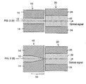
- FIG. 2 (A) shows a sectional view (central sectional view) taken on line A-A of the embodiment in FIG. 1 and
- FIG. 2 (B) shows a sectional view (cross sectional view) taken on line B-B of the embodiment in FIG. 1.
- a core part of the waveguide is illustrated as solid lines and the rest are illustrated as broken lines in FIG. 1.
- a core 12 of a silica optical waveguide 10 is originally a rectangle of 4.5 ⁇ m in depth and width, and a core 22 of a silica fiber 20 is 9 ⁇ m in diameter.
- both silica optical waveguide 10 and optical fiber 20 consist of a single mode optical waveguide.
- the refractive index of the core 12 of the silica optical waveguide 10 is 1.4657 and that of a clad 14 is 1.4440. Accordingly, the relative refractive index difference ⁇ is approximately 1.5 %.
- the refractive index of the core 22 of the silica optical fiber 20 is 1.4488 and that of a clad 24 is 1.4440. Accordingly, the relative refractive index difference ⁇ is approximately 0.33 %.
- the core 12 of the silica waveguide 10 and the core 22 of the silica optical fiber 20 meet at the side of the silica optical waveguide 10.
- the width of the core 12 of the silica optical waveguide 10 tapers in the longitudinal direction at a part 16 of approximately 1000 ⁇ m connecting to the optical fiber 20 as shown in FIG. 2(B).
- the tapered part 16 keeps a constant core width in thickness as shown in FIG. 2(A).
- the tip width of the core 12 is 0.5 ⁇ m for example.
- Such a tapered form of the core 12 can be easily obtained using a photolithograph method when the core 12 is formed on a quartz substrate.
- FIGS. 3 (A) through (F) depict field distributions in width and depth directions of each part of the silica optical waveguide 10 respectively. It is obvious from FIGS. 3 (A) through (F) that the field diameter becomes extremely smaller in width direction.
- FIGS. 3 (A) through (C) depict a field distribution in the depth direction respectively, and FIGS. 3(D) through (F) depict a field distribution of the width direction respectively.
- the vertical axis expresses relative optical intensity and the horizontal axis expresses relative values of distance.
- FIG. 4 shows coupling loss of the core 12 and the optical fiber 20 of TE mode when the tip width of the core 12 is varied.
- the horizontal axis expresses the width of the tip part of the core 12 and the vertical axis expresses the coupling loss. Understandably, it is preferable to have the smallest coupling loss. It is obvious from FIG. 4 that the coupling loss reduces as the tip width of the core 12 narrows, and even a coupling loss as low as 0.5 dB or less can be easily realized.
- the coupling loss becomes the minimum.
- the coupling loss is 1.02 dB, namely the loss is 20.9 %. This equals to the minimum value of coupling loss obtained through a high-order mode conversion of a conventional system to enlarge a core diameter.
- the coupling loss decreases even more when the tip width of the core 12 narrows to 2 ⁇ m or less.
- the coupling loss especially decreases as low as 0.40 dB, namely the loss is 8.8 % when the tip width narrows to 0.5 ⁇ m or less.
- the minimum coupling loss is substantially 0.40 dB.
- the tip width of the core 12 can be narrower as the manufacturing technique improves, there is a possibility that the coupling loss might become even lower.
- the core 12 which width and depth are constant, light propagates in a single mode with a mode field diameter of approximately 5 ⁇ m.
- the light since the width of the core 12 gradually narrows, the light also gradually converts to a radiation mode. Because the length of the taper part 16 is sufficient long as 1000 ⁇ m, the conversion from the fundamental guided mode to the radiation mode is adiabatically performed, and the loss due to the mode conversion becomes extremely low. The radiation mode is not shut in the core 12 and accordingly its MFD gradually increases. As shown in FIG. 3, although field patterns of the propagation light indicate slight differences between the width and thickness directions, both keep the forms that roughly approximate a Gaussian distribution.
- the average value of the MFD in the width and thickness directions becomes approximately 9.0 ⁇ m, which is close to the MFD (approximately 9.5 ⁇ m) of the optical fiber 20.
- the shape of the tapered part 16 is symmetrical relative to an optical axis. Therefore, the propagating direction of the radiation mode equals to that of the guided mode, and the propagating direction of the light does not change even after almost all the lights shifted to the radiation mode.
- the above-described things are considered as the reasons why the coupling loss decreases when the tip width of the core 12 extremely narrowed as shown in FIG. 4.
- the tip width of the core 12 is made even smaller, the light propagating the core 12 is finally launched as the radiation mode toward the outside.
- the side face of the silica optical waveguide 10 is tightly connected to the end face of the optical fiber 20 and also in view of the measured results shown in FIG. 4, assumably it does not increase the coupling loss with the optical fiber 20.
- FIG. 5 shows a plan view when this embodiment is applied to the optical coupling of a plane optical circuit composed of asymmetry Mach-Zehnder interferometer having paths of different optical path lengths and an optical fiber.
- Reference numeral 30 denotes a plane optical circuit made of mainly quartz on a quartz substrate and connected to optical fibers 32 and 34 at one end face and to optical fibers 36 and 38 at the other end face. A part near to the end face of a core of the plane optical circuit 30 is shaped to a tapered form as shown in FIGS. 1 and 2.
- this embodiment is applicable to an input and output of an arrayed waveguide grating besides the interference plane optical circuit 30 shown in FIG. 5.
- this embodiment exhibits even greater effectiveness.
- this embodiment is applicable to a multi-layer plane optical circuit in which plane optical circuits are layered.
- the tapered configuration functions to approximate both mode field diameters to make the optical coupling easy. Accordingly, a plane optical waveguide having a high ⁇ can be used, and thus it is possible to make an optical device to utilize it compact.
Landscapes
- Physics & Mathematics (AREA)
- General Physics & Mathematics (AREA)
- Optics & Photonics (AREA)
- Optical Integrated Circuits (AREA)
- Optical Couplings Of Light Guides (AREA)
Applications Claiming Priority (2)
| Application Number | Priority Date | Filing Date | Title |
|---|---|---|---|
| JP2001029521A JP3952696B2 (ja) | 2001-02-06 | 2001-02-06 | 光結合構造 |
| JP2001029521 | 2001-02-06 |
Publications (2)
| Publication Number | Publication Date |
|---|---|
| EP1229363A2 true EP1229363A2 (de) | 2002-08-07 |
| EP1229363A3 EP1229363A3 (de) | 2004-01-02 |
Family
ID=18893863
Family Applications (1)
| Application Number | Title | Priority Date | Filing Date |
|---|---|---|---|
| EP02000882A Withdrawn EP1229363A3 (de) | 2001-02-06 | 2002-01-15 | Optische Kopplungsstruktur |
Country Status (4)
| Country | Link |
|---|---|
| US (1) | US6801692B2 (de) |
| EP (1) | EP1229363A3 (de) |
| JP (1) | JP3952696B2 (de) |
| CA (1) | CA2369191A1 (de) |
Families Citing this family (17)
| Publication number | Priority date | Publication date | Assignee | Title |
|---|---|---|---|---|
| US20020051200A1 (en) | 2000-11-01 | 2002-05-02 | Chang William Ho | Controller for device-to-device pervasive digital output |
| US10860290B2 (en) | 2000-11-01 | 2020-12-08 | Flexiworld Technologies, Inc. | Mobile information apparatuses that include a digital camera, a touch sensitive screen interface, support for voice activated commands, and a wireless communication chip or chipset supporting IEEE 802.11 |
| US11204729B2 (en) | 2000-11-01 | 2021-12-21 | Flexiworld Technologies, Inc. | Internet based digital content services for pervasively providing protected digital content to smart devices based on having subscribed to the digital content service |
| US10915296B2 (en) | 2000-11-01 | 2021-02-09 | Flexiworld Technologies, Inc. | Information apparatus that includes a touch sensitive screen interface for managing or replying to e-mails |
| US7953818B2 (en) | 2000-11-20 | 2011-05-31 | Flexiworld Technologies, Inc. | Output device and system for rendering digital content |
| US20020097417A1 (en) | 2001-01-19 | 2002-07-25 | Chang William Ho | System for universal data output |
| US7221826B2 (en) * | 2002-10-08 | 2007-05-22 | Tdk Corporation | Spot-size transformer, method of producing spot-size transformer and waveguide-embedded optical circuit using spot-size transformer |
| JP2004170924A (ja) * | 2002-11-05 | 2004-06-17 | Tdk Corp | 導波路埋め込み型光回路及びこれに用いる光学素子 |
| EP1639679B1 (de) * | 2003-06-16 | 2008-07-02 | Soreq Nuclear Research Center | Optische vorrichtung |
| JP2006317572A (ja) * | 2005-05-11 | 2006-11-24 | Photonic Science Technology Inc | 光導波路及びその製造方法 |
| US8078020B2 (en) * | 2008-04-08 | 2011-12-13 | Alcatel Lucent | Optical mode-converter structure |
| JP2016106238A (ja) * | 2013-03-25 | 2016-06-16 | 技術研究組合光電子融合基盤技術研究所 | 光結合構造及び光モジュール |
| CN106461873B (zh) * | 2014-04-30 | 2021-04-20 | 华为技术有限公司 | 低损耗模转换器及其制作方法 |
| US9563018B2 (en) | 2014-10-09 | 2017-02-07 | International Business Machines Corporation | Tapered photonic waveguide to optical fiber proximity coupler |
| JP6649843B2 (ja) * | 2016-05-13 | 2020-02-19 | Nttエレクトロニクス株式会社 | 光回路 |
| JP2018097012A (ja) * | 2016-12-07 | 2018-06-21 | 学校法人慶應義塾 | スポットサイズ変換器、及びその製造方法 |
| CN116520491B (zh) * | 2023-05-10 | 2025-08-19 | 北方集成电路技术创新中心(北京)有限公司 | 一种端面耦合器结构及其形成方法 |
Family Cites Families (9)
| Publication number | Priority date | Publication date | Assignee | Title |
|---|---|---|---|---|
| JP2929481B2 (ja) * | 1992-05-20 | 1999-08-03 | 日本電信電話株式会社 | 光機能素子 |
| US5515464A (en) * | 1992-07-06 | 1996-05-07 | Sheem Sang K | Optical fiber interconnections using self-aligned core-extensions |
| JPH0784146A (ja) * | 1993-09-16 | 1995-03-31 | Hitachi Cable Ltd | 接続用光素子、その製造方法及び光素子の接続方法 |
| US5844929A (en) * | 1994-02-24 | 1998-12-01 | British Telecommunications Public Limited Company | Optical device with composite passive and tapered active waveguide regions |
| JPH08330671A (ja) * | 1995-05-31 | 1996-12-13 | Hitachi Ltd | 半導体光素子 |
| US6229947B1 (en) * | 1997-10-06 | 2001-05-08 | Sandia Corporation | Tapered rib fiber coupler for semiconductor optical devices |
| JP2000304964A (ja) * | 1999-04-23 | 2000-11-02 | Japan Aviation Electronics Industry Ltd | 光結合装置 |
| JP2000332350A (ja) * | 1999-05-19 | 2000-11-30 | Hitachi Cable Ltd | グレーティング導波路一体型アクティブデバイス |
| JP3059171B1 (ja) * | 1999-09-14 | 2000-07-04 | 株式会社東芝 | 光ファイバ出力半導体装置 |
-
2001
- 2001-02-06 JP JP2001029521A patent/JP3952696B2/ja not_active Expired - Fee Related
-
2002
- 2002-01-15 EP EP02000882A patent/EP1229363A3/de not_active Withdrawn
- 2002-01-23 CA CA002369191A patent/CA2369191A1/en not_active Abandoned
- 2002-02-04 US US10/067,552 patent/US6801692B2/en not_active Expired - Lifetime
Non-Patent Citations (7)
| Title |
|---|
| "Corning SMF-28 optical fiber" CORNING PRODUCT INFORMATION, XX, XX, April 2001 (2001-04), pages 1-4, XP002960626 * |
| GOODWILL D J ET AL: "Polymer tapered waveguides and flip-chip solder bonding as compatible technologies for efficient OEIC coupling" ELECTRONIC COMPONENTS AND TECHNOLOGY CONFERENCE, 1997. PROCEEDINGS., 47TH SAN JOSE, CA, USA 18-21 MAY 1997, NEW YORK, NY, USA,IEEE, US, 18 May 1997 (1997-05-18), pages 788-796, XP010233930 ISBN: 0-7803-3857-X * |
| LIERSTUEN L O ET AL: "COUPLING LOSSES BETWEEN STANDARD SINGLE-MODE FIBERS AND RECTANGULARWAVEGUIDES FOR INTEGRATED OPTICS" APPLIED OPTICS, OPTICAL SOCIETY OF AMERICA,WASHINGTON, US, vol. 34, no. 6, 20 February 1995 (1995-02-20), pages 1024-1028, XP000490004 ISSN: 0003-6935 * |
| M[RZ, REINHARD: "Integrated Optics: Design and Modelling" 1995 , ARTECH HOUSE , NORWOOD, MA 02062 XP002258513 * chapter 1.2 * * |
| MITOMI O ET AL: "DESIGN OF A SINGLE-MODE TAPERED WAVEGUIDE FOR LOW-LOSS CHIP-TO-FIBRE COUPLING" IEEE JOURNAL OF QUANTUM ELECTRONICS, IEEE INC. NEW YORK, US, vol. 30, no. 8, 1 August 1994 (1994-08-01), pages 1787-1793, XP000465440 ISSN: 0018-9197 * |
| MOERMAN I ET AL: "III-V SEMICONDUCTOR WAVEGUIDING DEVICES USING ADIABATIC TAPERS" MICROELECTRONICS JOURNAL, MACKINTOSH PUBLICATIONS LTD. LUTON, GB, vol. 25, no. 8, 1994, pages 675-690, XP001149912 ISSN: 0026-2692 * |
| RAJARAJAN M ET AL: "NUMERICAL STUDY OF SPOT-SIZE EXPANDERS FOR AN EFFICIENT OEIC TO SMFCOUPLING" IEEE PHOTONICS TECHNOLOGY LETTERS, IEEE INC. NEW YORK, US, vol. 10, no. 8, 1 August 1998 (1998-08-01), pages 1082-1084, XP000769863 ISSN: 1041-1135 * |
Also Published As
| Publication number | Publication date |
|---|---|
| US6801692B2 (en) | 2004-10-05 |
| CA2369191A1 (en) | 2002-08-06 |
| EP1229363A3 (de) | 2004-01-02 |
| JP2002228863A (ja) | 2002-08-14 |
| JP3952696B2 (ja) | 2007-08-01 |
| US20020106159A1 (en) | 2002-08-08 |
Similar Documents
| Publication | Publication Date | Title |
|---|---|---|
| US6801692B2 (en) | Optical coupling structure | |
| CN102159975B (zh) | 用于在硅光子芯片与光纤之间有效耦合的方法和设备 | |
| US6628859B2 (en) | Broadband mode converter | |
| US6353694B1 (en) | MMI thermo-optic coupler | |
| US5515464A (en) | Optical fiber interconnections using self-aligned core-extensions | |
| US6563988B2 (en) | Optical apparatus and method having predetermined group velocity dispersion | |
| CN100437176C (zh) | 偏振补偿的光分路器 | |
| US6404946B1 (en) | Arrayed waveguide grating type optical multiplexer/demultiplexer | |
| JP3139571B2 (ja) | 光合分波器 | |
| US8615146B2 (en) | Planar optical waveguide | |
| JP3039491B2 (ja) | 光波長合分波器 | |
| US6798952B2 (en) | Optical multiplexer/demultiplexer | |
| KR102364302B1 (ko) | 평탄한 모드 발생 장치 및 이를 구비하는 배열 도파로 격자 | |
| JP2001174653A (ja) | アレイ導波路格子 | |
| EP1128193A1 (de) | Wellenleiterarraybeugungsgitter | |
| JP2861996B1 (ja) | 光波長合分波器 | |
| JP2000171663A (ja) | クラッドモ―ド結合器とブラッグファイバ格子で形成されるアッド/ドロップフィルタ―及びマルチプレクサ | |
| CN100394233C (zh) | 光纤耦合器及其中的光纤 | |
| KR20000014362A (ko) | 열광학 효과를 이용한 집적광학형 가변 광감쇄기 | |
| KR20050092286A (ko) | 고차 모드 제거 필터링 기능을 갖는 단일모드 광섬유 구조 | |
| KR101423978B1 (ko) | 열광학 가변 광감쇄기 | |
| CN119667978B (zh) | 一种基于薄膜铌酸锂光波导的宽带光子滤波器 | |
| JP2000321449A (ja) | 導波路型光合分波回路チップ | |
| CN120469001A (zh) | 一种基于氮化硅波导的双偏振多模马赫增德尔干涉仪 | |
| GB2360098A (en) | Optical waveguide array device |
Legal Events
| Date | Code | Title | Description |
|---|---|---|---|
| PUAI | Public reference made under article 153(3) epc to a published international application that has entered the european phase |
Free format text: ORIGINAL CODE: 0009012 |
|
| AK | Designated contracting states |
Kind code of ref document: A2 Designated state(s): AT BE CH CY DE DK ES FI FR GB GR IE IT LI LU MC NL PT SE TR |
|
| AX | Request for extension of the european patent |
Free format text: AL;LT;LV;MK;RO;SI |
|
| PUAL | Search report despatched |
Free format text: ORIGINAL CODE: 0009013 |
|
| AK | Designated contracting states |
Kind code of ref document: A3 Designated state(s): AT BE CH CY DE DK ES FI FR GB GR IE IT LI LU MC NL PT SE TR |
|
| AX | Request for extension of the european patent |
Extension state: AL LT LV MK RO SI |
|
| STAA | Information on the status of an ep patent application or granted ep patent |
Free format text: STATUS: THE APPLICATION HAS BEEN WITHDRAWN |
|
| 18W | Application withdrawn |
Effective date: 20040630 |